 | –≠–ª–µ–∫—Ç—Ä–æ–Ω–Ω—ã–π –∫–æ–º–ø–æ–Ω–µ–Ω—Ç: ADM869L | –°–∫–∞—á–∞—Ç—å:  PDF PDF  ZIP ZIP |
REV. A
Information furnished by Analog Devices is believed to be accurate and
reliable. However, no responsibility is assumed by Analog Devices for its
use, nor for any infringements of patents or other rights of third parties
which may result from its use. No license is granted by implication or
otherwise under any patent or patent rights of Analog Devices.
a
ADM869L
One Technology Way, P.O. Box 9106, Norwood, MA 02062-9106, U.S.A.
Tel: 781/329-4700
World Wide Web Site: http://www.analog.com
Fax: 781/326-8703
© Analog Devices, Inc., 2000
2 A, High-Side P-Channel Switch with
Current Limit and Thermal Shutdown
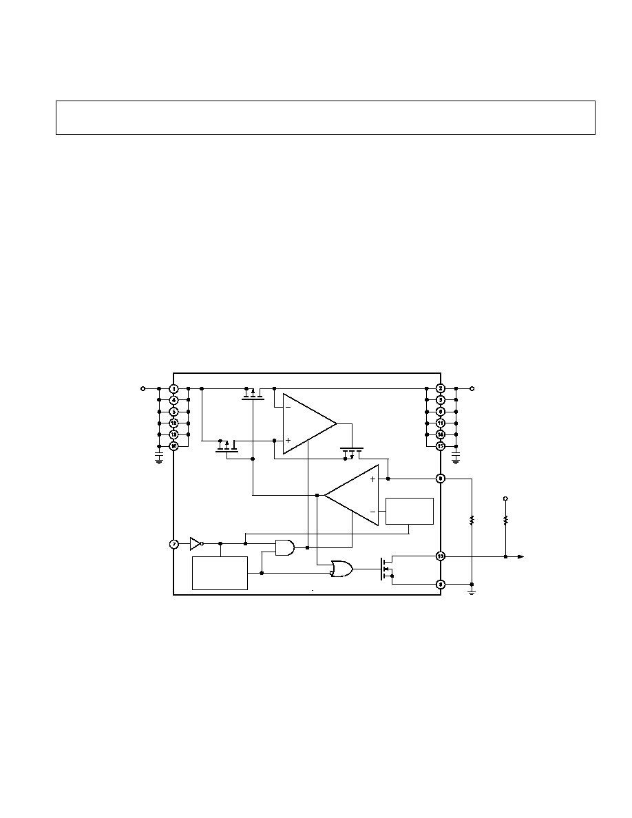
FUNCTIONAL BLOCK DIAGRAM
TEMPERATURE
SENSOR AND
CONTROL
CIRCUITRY
MAIN FET
MIRROR FET
IN
(2.7V TO 5.5V)
OUT
R
SET
SET
FAULT
GND
ON
R
PULLUP
10k TO 100k
V
PULLUP
0 TO 5.5V
ON
ON
ON
ON
OVERTEMP
ADM869L
CURRENT
LIMIT
AMPLIFIER
1.24V
BANDGAP
REFERENCE
MIRROR
AMPLIFIER
0.1 F
22 F
FEATURES
2 A Load Current
45 m On Resistance
User-Settable Current Limit
12 A Typical Quiescent Current
10 nA Typical Shutdown Current
40 nA Typical Switch Off Leakage
Short-Circuit Protection
Thermal Shutdown
FAULT Output
Small, 16-Lead QSOP Package
APPLICATIONS
Desktop Computers
Palmtop Computers
Notebook Computers
Hand-Held Instruments
Universal Serial Bus (USB)
GENERAL DESCRIPTION
The ADM869L is a logic controlled P-channel switch with low
on resistance, capable of sourcing up to 2 A from supply voltages
between 2.7 V and 5.5 V. A user-settable current limit allows
the trip current to be set between 400 mA and 2 A with an
accuracy of
±21%. This allows the system power supply to be
protected against short circuits and surge currents in peripheral
loads powered via the ADM869L. Over-current and over-
temperature conditions are signalled by a
FAULT output.
The ADM869L also offers low quiescent current of typically
12
µA and shutdown current of typically 10 nA.
REV. A
≠2≠
ADM869L≠SPECIFICATIONS
(V
CC
= 3.0 V, T
A
= ≠40 C to +85 C
1
, unless otherwise noted.)
Parameter
Min
Typ
Max
Unit
Test Conditions/Comments
Operating Voltage Range
2.7
5.5
V
Quiescent Current
12
20
µA
V
IN
= 5 V,
ON = GND, I
OUT
= 0 A,
0
∞C to 85∞C
12
25
µA
V
IN
= 5 V,
ON = GND, I
OUT
= 0 A,
≠40
∞C to +85∞C
Shutdown Supply Current
0.01
2
µA
ON = V
IN
= V
OUT
= 5.5 V
Off-Switch Current
0.04
2
µA
ON = V
IN
= V
CC
, V
OUT
= 0 V
Undervoltage Lockout
2.0
2.3
2.6
V
Rising Edge, 1% Hysteresis
On Resistance
38
70
m
V
IN
= 4.75 V
45
90
m
V
IN
= 3.0 V
Nominal Current-Limit Setting Range
0.4
2.4
A
R
SET
= 1% Tolerance
2
Current-Limit Amplifier Threshold
1.178
1.240
1.302
V
V
SET
Required to Turn Off Switch
3
I
OUT
/I
SET
Current Ratio
810
955
1100
A/A
I
OUT
= 1 A, V
OUT
> 1.6 V
ON Input Low Voltage, V
IL
0.8
V
V
IN
= 2.7 V to 5.5 V
ON Input High Voltage, V
IH
2.0
V
V
IN
= 2.7 V to 3.6 V
2.4
V
V
IN
= 4.5 V to 5.5 V
ON Input Leakage
0.01
±1
µA
V
ON
= 5.5 V
Current-Limit Amplifier Input Bias Current
0.05
±3
µA
V
SET
= 1.24 V, I
OUT
= 0 A
FAULT Logic Output Low Voltage
0.4
V
I
SINK
= 1 mA, V
SET
= 1.4 V
FAULT Output High Leakage Current
0.05
1
µA
V
FAULT
= 5.5 V, V
SET
= 1 V
Slow Current-Loop Response Time
10
µs
20% Current Overdrive, V
IN
= 5 V
Fast Current-Loop Response Time
4
µs
Turn-On Time
100
300
µs
V
IN
= 5 V, I
OUT
= 500 mA
200
µs
V
IN
= 3 V, I
OUT
= 500 mA
Turn-Off Time
1
2
30
µs
V
IN
= 5 V, I
OUT
= 500 mA
NOTES
1
Specifications to ≠40
∞C are guaranteed by design, not tested.
2
Guaranteed by design. Derived from the I
SET
current ratio, current-limit amplifier and external set resistor accuracies.
3
Tested with I
OUT
= 200 mA and V
SET
adjusted until (V
IN
≠ V
OUT
) 0.8 V.
Specifications subject to change without notice.
REV. A
ADM869L
≠3≠
PIN CONFIGURATION
1
2
3
4
5
6
7
8
IN
OUT
OUT
OUT
IN
16
15
14
13
12
9
10
11
ADM869L
TOP VIEW
(Not to Scale)
OUT
IN
IN
IN
IN
OUT
GND
OUT
FAULT
SET
ON
ABSOLUTE MAXIMUM RATINGS
*
(T
A
= 25
∞C unless otherwise noted)
IN to GND . . . . . . . . . . . . . . . . . . . . . . . . . . . ≠0.3 V to +6 V
ON, FAULT to GND . . . . . . . . . . . . . . . . . . . ≠0.3 V to +6 V
SET, OUT to GND . . . . . . . . . . . . . . ≠0.3 V to (V
IN
+ 0.3 V)
Maximum Continuous Switch Current . . . . . . . . . . . . . . . 3 A
Continuous Power Dissipation (T
A
= 70
∞C) . . . . . . . 667 mW
QSOP (Derate 8.3 mW/
∞C above 70∞C)
Operating Temperature Range
Industrial (A Version) . . . . . . . . . . . . . . . . ≠40
∞C to +85∞C
Storage Temperature Range . . . . . . . . . . . . ≠65
∞C to +150∞C
Lead Temperature (Soldering, 10 sec) . . . . . . . . . . . . . 300
∞C
ESD Rating (Outputs) . . . . . . . . . . . . . . . . . . . . . . . . . . 15 kV
(Other Pins) . . . . . . . . . . . . . . . . . . . . . . . . . . . . . . . . . 2 kV
*This is a stress rating only; functional operation of the device at these or any other
conditions above those indicated in the operation sections of this specification is
not implied. Exposure to absolute maximum rating conditions for extended
periods of time may affect reliability.
THERMAL CHARACTERISTICS
16-Lead QSOP Package:
JA
= 50
∞C/W,
JC
= 10
∞C/W
ORDERING GUIDE
Temperature
Package
Package
Model
Range
Description
Option
ADM869LARQ ≠40
∞C to +85∞C 16-Lead QSOP RQ-16
PIN FUNCTION DESCRIPTIONS
Pin
Mnemonic
Function
1, 4, 5, 12, 13, 16
IN
Input to P-Channel MOSFET Source and Supply to Chip Circuitry. Bypass IN with a 22
µF
capacitor to ground.
2, 3, 6, 11, 14, 15
OUT
Output from P-Channel MOSFET Drain. Bypass OUT with a 0.1
µF capacitor to ground.
7
ON
Digital Input. Active-low switch enable (logic 0 turns the switch on).
9
SET
Current Limit Setting Input. A resistor from set to ground sets the current limit. Refer to
Current Limit section.
10
FAULT
Open-Drain Digital Output.
FAULT goes low when the current limit is exceeded or the die
temperature exceeds 135
∞C. During startup, FAULT remains low for the turn-on time + 50 µs.
REV. A
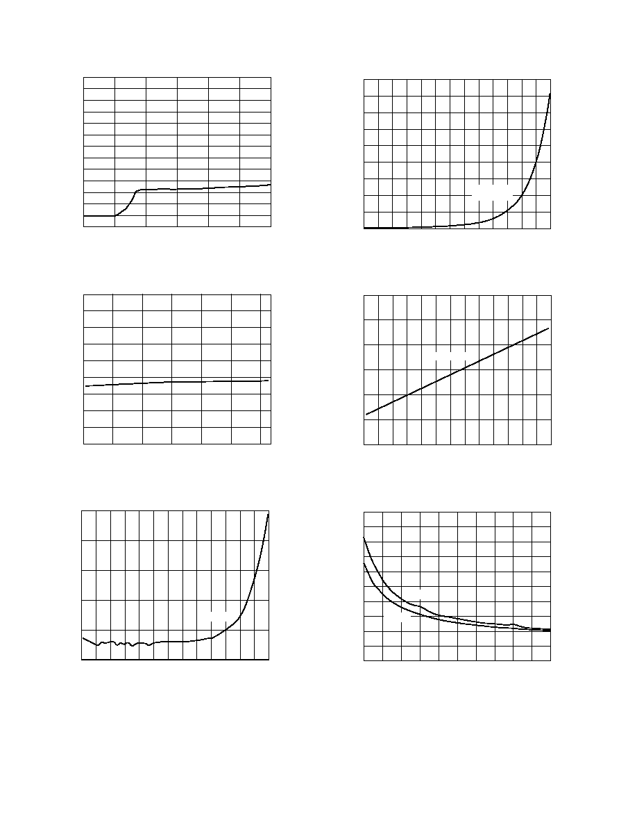
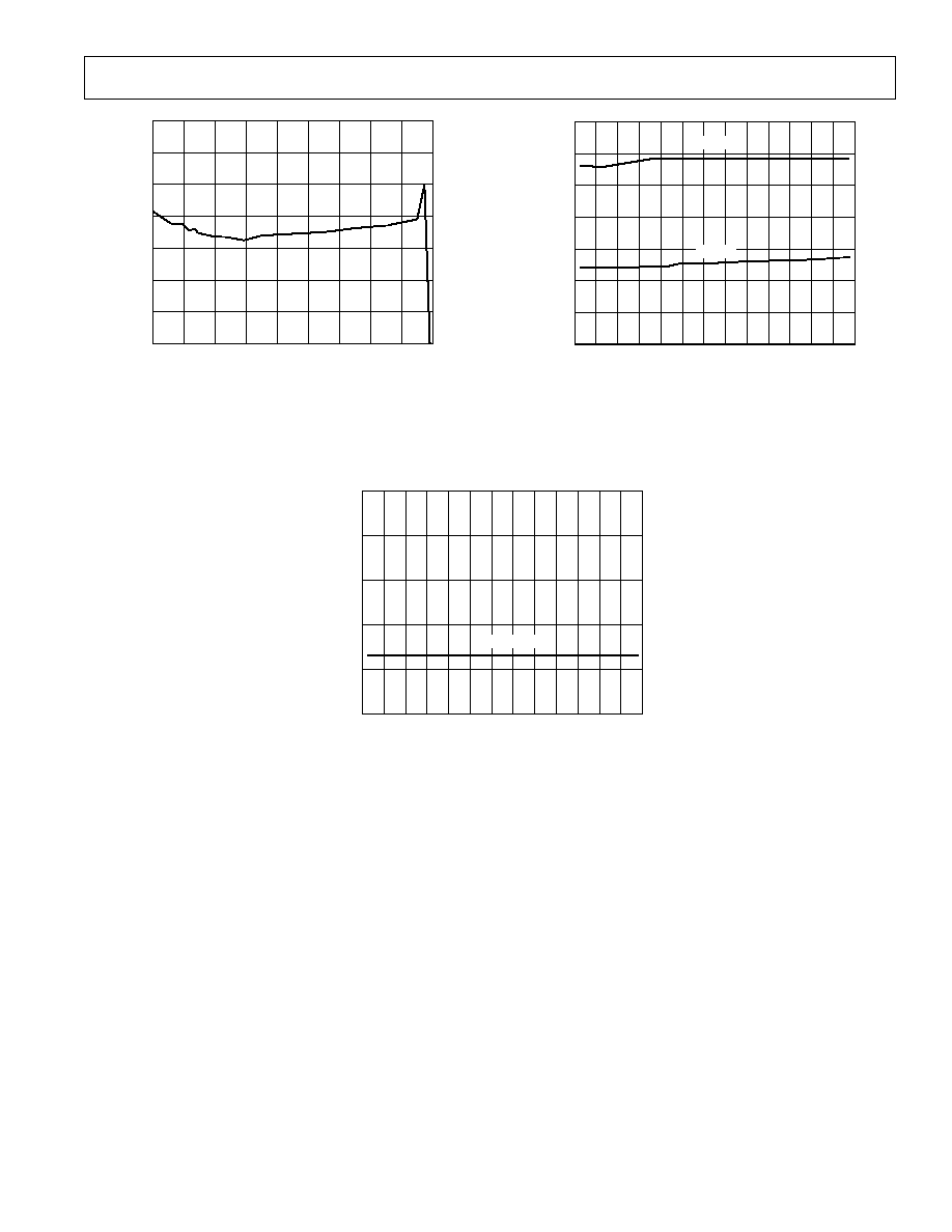
ADM869L≠Typical Performance Characteristics
≠4≠
INPUT VOLTAGE ≠ Volts
QUIESCENT CURRENT ≠
A
≠5
15
5
0
6
1
2
4
5
3
0
20
25
30
35
40
45
50
55
60
10
TPC 1. Quiescent Current vs. Input Voltage
TEMPERATURE ≠ C
CURRENT
≠
A
10.0
≠40
11.5
13.0
≠20
0
20
40
60
80
12.5
12.0
10.5
11.0
TPC 2. Quiescent Current vs. Temperature
TEMPERATURE ≠ C
CURRENT
≠
nA
≠1
≠40
CURRENT
≠20
0
20
40
60
80
1
3
5
7
9
TPC 3. Off-Supply Current vs. Temperature
TEMPERATURE ≠ C
CURRENT
≠
nA
0
≠40
OFF-SWITCH
CURRENT
≠20
0
20
40
60
80
5
10
15
20
25
30
35
40
45
TPC 4. Off-Switch Current vs. Temperature
TEMPERATURE ≠ C
NORMALIZED R
ON
0.7
≠40
RESISTANCE
≠20
0
20
40
60
80
0.8
0.9
1.0
1.1
1.2
1.3
TPC 5. Normalized On Resistance vs. Temperature
I
SWITCH
≠ A
I
OUT
/I
SET
RATIO
800
0.4
V
IN
= 5V
0.6
1.0
1.4
1.8
2.2
V
IN
= 3V
850
900
950
1000
1050
1100
1150
1200
0.8
2.4
2.0
1.6
1.2
1250
1300
TPC 6. I
OUT
/I
SET
Ratio vs. Switch Current
REV. A
ADM869L
≠5≠
OUTPUT VOLTAGE
NORMALIZED OUTPUT CURRENT
0
0.5
1.0
1.5
2.0
2.5
3.0
3.5
4.0
4.5
5.0
0.2
0.4
0.6
0.8
1.0
1.2
1.4
TPC 7. Normalized Output Current vs. Output Voltage
TEMPERATURE ≠ C
t
ON
≠
s
0
≠40
V
IN
= 3V
≠20
0
20
40
60
80
50
100
150
200
250
300
350
V
IN
= 5V
TPC 8. Turn-On Time vs. Temperature
TEMPERATURE ≠ C
t
OFF
≠
s
0
≠40
V
IN
= 3V OR 5V
≠20
0
20
40
60
80
1
2
3
4
5
TPC 9. Turn-Off Time vs. Temperature
REV. A
ADM869L
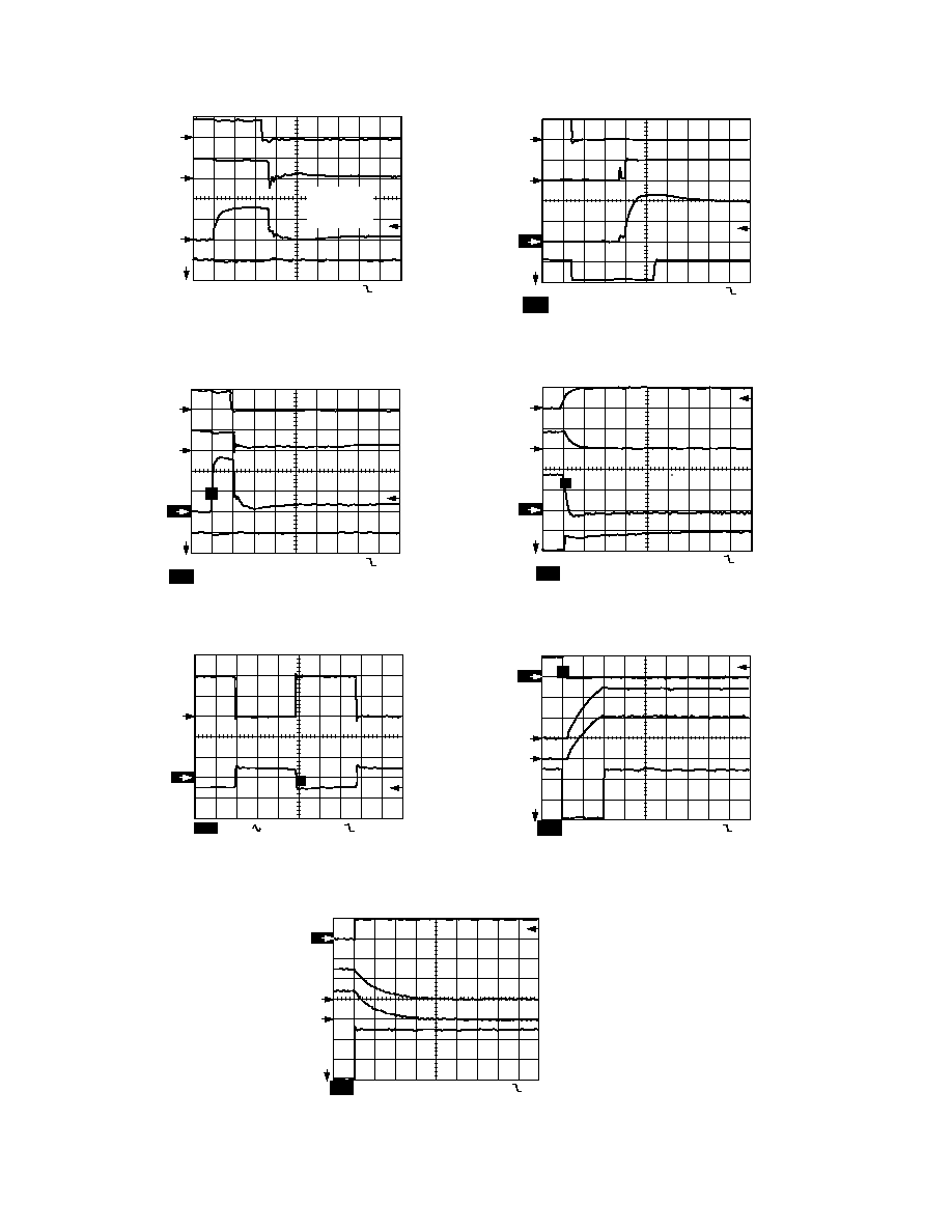
≠6≠
CH3
CH1
5.00V CH2 2.00V M 500 s CH1
3.1V
4
2
1
100mV CH4 2.00V
3
T
T
T
V
ON
V
OUT
I
OUT,
0.5A/DIV
V
FAULT
TPC 16. USB Circuit Output Fall Time
CH1
5.00V CH2 5.00V M 20.0 s CH3
120mV
V
FAULT
, 5V/DIV
I
OUT
, 4A/DIV
V
OUT
, 5V/DIV
V
IN
, 5V/DIV
4
3
2
1
C
IN
= 100 F
C
OUT
= 0.1 F
R
LOAD
= 1.0
TPC 10. Fast Current-Limit Response
V
FAULT
, 5V/DIV
I
OUT
, 2A/DIV
V
OUT
, 5V/DIV
V
IN
, 5V/DIV
4
2
1
3
CH3
CH1 5.00V
CH2 5.00V M 50.0 s CH3
64mV
100mV
CH4 5.00V
B
W
T
T
T
TPC 11. Slow Current-Limit Response
I
OUT
= 0mA TO
1A, 0.5A/DIV
V
OUT
RIPPLE,
100mV/DIV,
AC COUPLED
3
2
CH2
CH3 50.0mV
100mV
M 10.0 s CH2
≠52mV
B
W
B
W
T
T
TPC 12. Load Transient Response
3
CH3
CH1
5.00V
CH2 5.00V M 50.0 s CH1
2.2V
4
2
1
50.0mV
CH4 5.00V
B
W
V
ON
V
OUT
I
OUT,
0.5A/DIV
V
FAULT
TPC 13. Switch Turn-On Time
3
CH3
CH1
5.00V CH2 5.00V M 1.00 s CH1
2.5V
4
2
1
100mV CH4 5.00V
T
T
T
T
V
ON
V
OUT
I
OUT,
0.5A/DIV
V
FAULT
TPC 14. Switch Turn-Off Time
CH3
CH1
5.00V CH2 2.00V M 500 s CH1
3.1V
4
2
1
100mV CH4 2.00V
3
T
T
T
T
V
ON
V
OUT
I
OUT,
0.5A/DIV
V
FAULT
TPC 15. USB Circuit Output Rise Time
REV. A
ADM869L
≠7≠
FUNCTIONAL DESCRIPTION
The ADM869L comprises a high-current P-channel switch con-
trolled by an active-low logic input
ON (Pin 7). When ON is
low, the internal circuitry of the ADM869 is powered up and the
output of the current-limit amplifier is low, providing gate drive
to the switching FET. When
ON is high, the internal circuitry is
powered down and the current consumption is typically 100 nA.
It should be noted that the ADM869L is not a bidirectional
switch, so V
IN
must always be higher than V
OUT
.
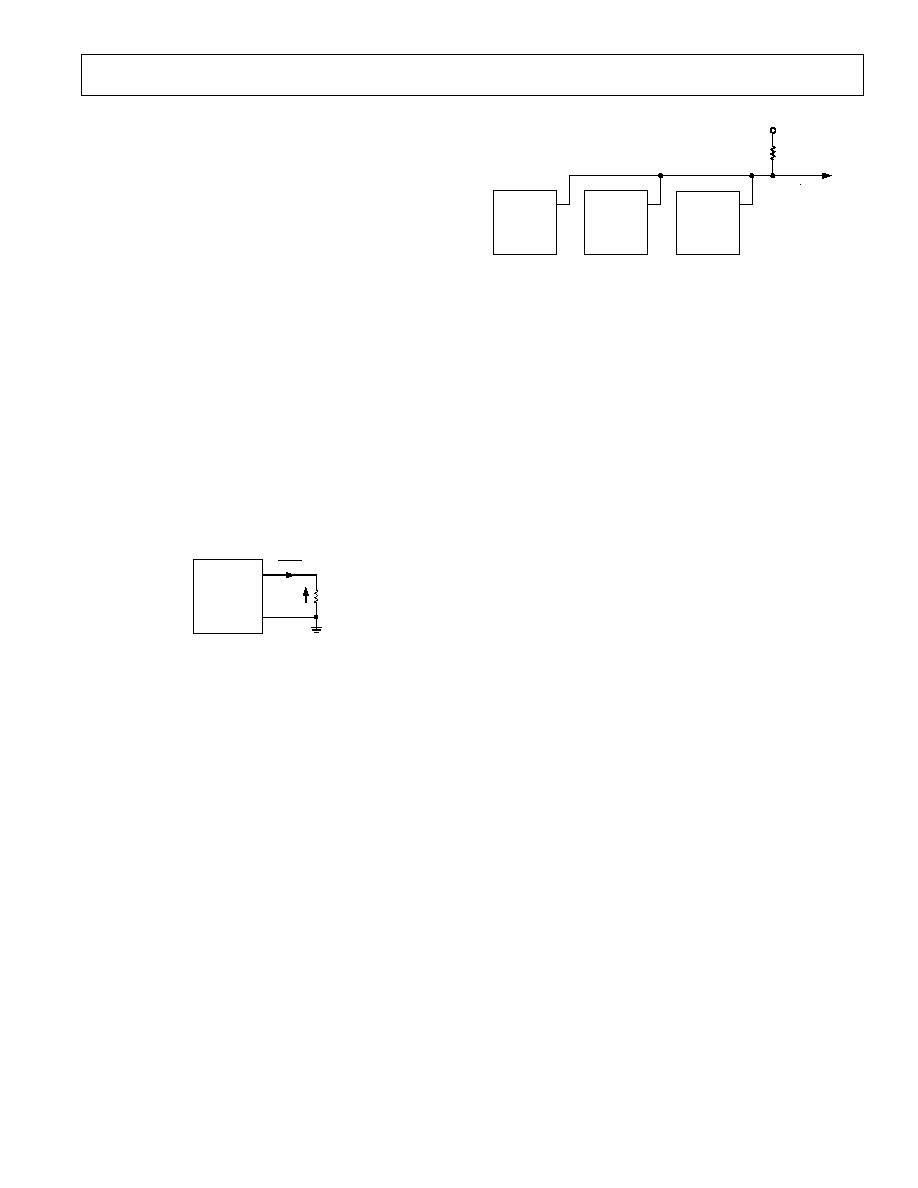
CURRENT LIMIT
When the switch is turned on, a smaller mirror switch passes a
proportionate current equal to I
OUT
/955. The mirror amplifier
maintains this relationship by keeping the drain of the mirror
FET at the same voltage as the main FET, and drives the mirror
current through the current-limit resistor RSET, which is
connected between the noninverting input of the current limit
amplifier and ground. An on-chip bandgap reference of 1.24 V
is connected to the inverting input of the current-limit amplifier.
When the load current exceeds the preset limit, the voltage
across R
SET
exceeds 1.24 V, and the output voltage of the
current-limit amplifier rises, reducing the gate drive to the FETs.
If, for example, a 1 A current limit is required, R
SET
= 1.24 V/
1.047 mA = 1.184 k
. Note that I
OUT
/I
SET
varies depending on
current so please refer to TPC 6.
ADM869L
SET
R
SET
1.24V
I
LIMIT
955
Figure 1. Setting the Current Limit
THERMAL SHUTDOWN
The thermal shutdown operates when the die temperature
exceeds 135
∞C, turning off the switch. The thermal shutdown
circuit has built-in hysteresis of 10
∞C, so the switch will not turn
on again until the die temperature falls to 125
∞C. If the fault
condition is not removed, the switch will pulse on and off as the
temperature cycles between these limits.
FAULT OUTPUT
If either the current limit or the thermal shutdown is activated,
FAULT will pull low. This is an open-drain output and requires
a pull-up resistor of between 10 k
and 100 k. Several FAULT
outputs may be wire-OR'd to form a common interrupt line, as
shown in Figure 2 or
FAULT may be wire-OR'd to an existing
interrupt line that has a resistive pull-up.
ADM869L
FAULT
R
PULLUP
V
PULLUP
INT
ADM869L
FAULT
ADM869L
FAULT
Figure 2. Wire Or'ing
FAULT Outputs
During startup, the
FAULT output goes low for the turn-on time
plus 50
µs.
APPLICATIONS INFORMATION
INPUT FILTERING
To prevent the input voltage being pulled below the minimum
operating voltage under transient short-circuit conditions, before
the current limit has had time to operate, a reservoir capacitor
should be connected from IN to GND. This does not need to be
large, but should have a low ESR. A 22
µF ceramic type is
suitable. Larger values will reduce the voltage drop still further.
OUTPUT CAPACITANCE
A 0.1
µF capacitor should be connected between OUT and
GND to prevent the back e.m.f. of parasitic inductance from
pulling OUT below ground during turn-off. For Universal Serial
Bus (USB) applications, C
OUT
should be at least 120
µF. This
causes the output rise and fall times to be longer, as shown in
the typical operating characteristics, but does not affect the
turn-off time of the ADM869L itself.
LAYOUT CONSIDERATIONS
Printed circuit board tracks to and from the ADM869L should be
as thick and as short as possible to minimize parasitic inductance
and take full advantage of the fast response time of the switch. It is
recommended that all input lines be connected together, close to
the device. This ensures equal current distribution in all legs. If
this is not possible, then all traces should be of equal width and
length. The same rules apply for all output lines. Input and output
capacitors should be placed as close to the device as possible (less
than 5 mm).
THERMAL CONSIDERATIONS
Under normal operating conditions, the worst-case power dissi-
pation will be 518 mW with the highest specified on resistance
and 3 V supply (W = 2.4 A
◊ 0.9 V). The package is capable of
handling and dissipating this power, but heat dissipation can
further be improved by providing a large area of copper in con-
tact with the device pins, particularly IN and OUT.
REV. A
≠8≠
C01037≠0≠7/00 (rev. A)
PRINTED IN U.S.A.
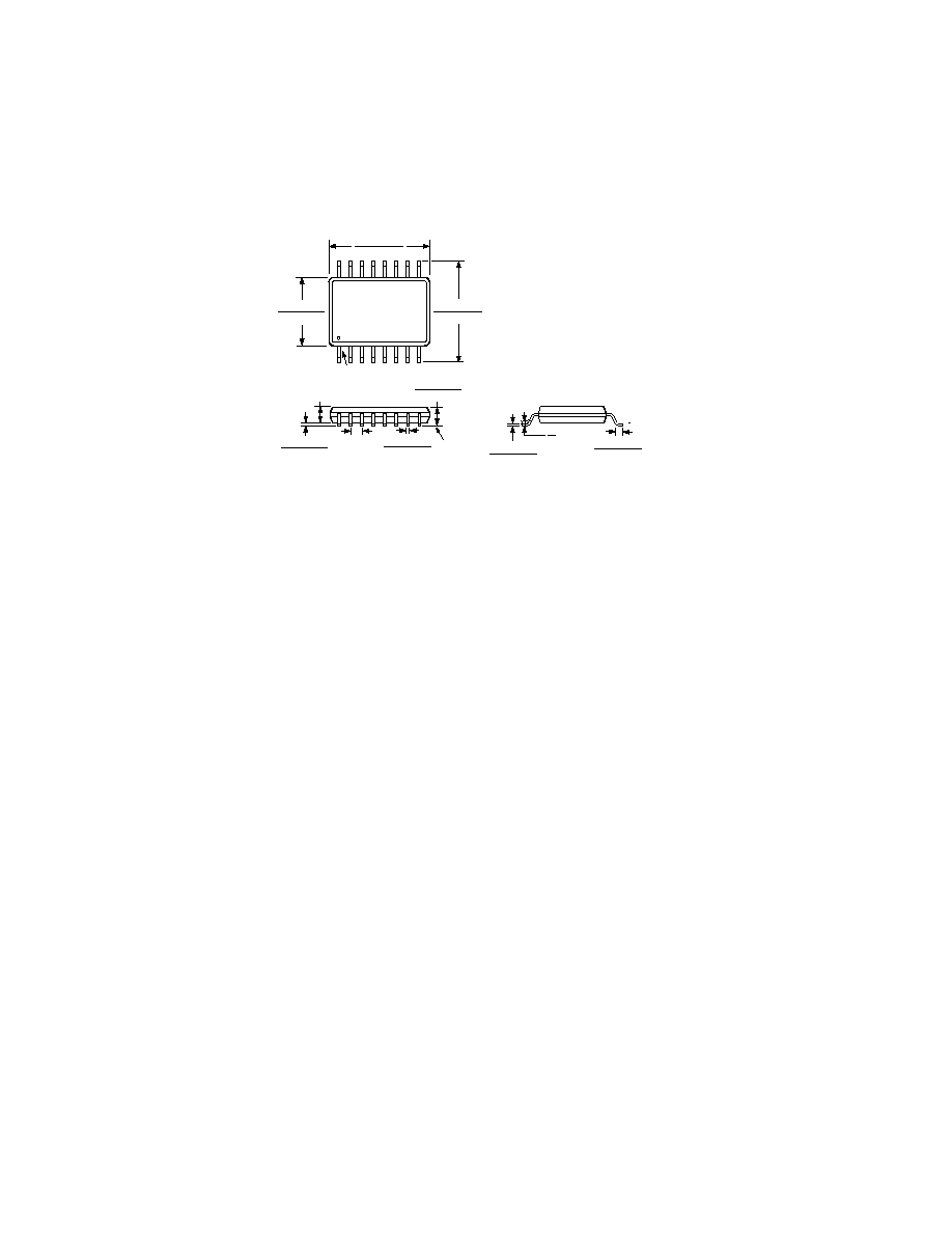
ADM869L
OUTLINE DIMENSIONS
Dimensions shown in inches and (mm).
16-Lead QSOP Package
(RQ-16)
16
9
8
1
0.197 (5.00)
0.189 (4.80)
0.244 (6.20)
0.228 (5.79)
PIN 1
0.157 (3.99)
0.150 (3.81)
SEATING
PLANE
0.010 (0.25)
0.004 (0.10)
0.012 (0.30)
0.008 (0.20)
0.025
(0.64)
BSC
0.059 (1.50)
MAX
0.069 (1.75)
0.053 (1.35)
0.010 (0.20)
0.007 (0.18)
0.050 (1.27)
0.016 (0.41)
8
0