 | –≠–ª–µ–∫—Ç—Ä–æ–Ω–Ω—ã–π –∫–æ–º–ø–æ–Ω–µ–Ω—Ç: ADN2830 | –°–∫–∞—á–∞—Ç—å:  PDF PDF  ZIP ZIP |
Document Outline
- FEATURES
- APPLICATIONS
- GENERAL DESCRIPTION
- FUNCTIONAL BLOCK DIAGRAM
- SPECIFICATIONS
- ABSOLUTE MAXIMUM RATINGS
- ORDERING GUIDE
- PIN CONFIGURATION
- PIN FUNCTION DESCRIPTIONS
- GENERAL
- CONTROL
- LOOP BANDWIDTH SELECTION
- ALARMS
- MONITOR CURRENTS
- AUTOMATIC LASER SHUTDOWN
- MODE
- ALARM INTERFACES
- POWER CONSUMPTION
- OUTLINE DIMENSIONS
- REVISION HISTORY

a
ADN2830
Information furnished by Analog Devices is believed to be accurate and
reliable. However, no responsibility is assumed by Analog Devices for its
use, nor for any infringements of patents or other rights of third parties that
may result from its use. No license is granted by implication or otherwise
under any patent or patent rights of Analog Devices. Trademarks and
registered trademarks are the property of their respective companies.
One Technology Way, P.O. Box 9106, Norwood, MA 02062-9106, U.S.A.
Tel: 781/329-4700
www.analog.com
Fax: 781/326-8703
© 2003 Analog Devices, Inc. All rights reserved.
REV. A
REV. A
Continuous Wave Laser
FUNCTIONAL BLOCK DIAGRAM
GND
GND
PAVCAP
V
CC
MPD
IBMON
IMPDMON
ALS
FAIL
DEGRADE
V
CC
GND
CONTROL
GND
IMPD
R
PSET
IBIAS
GND
RASET
MODE
V
CC
LD
PSET
ASET
FEATURES
Bias Current Range 4 mA to 200 mA
Monitor Photodiode Current 50 A to 1200 A
Closed-Loop Control of Average Power
Laser FAIL and Laser DEGRADE Alarms
Automatic Laser Shutdown, ALS
Full Current Parameter Monitoring
5 V Operation
≠40 C to +85 C Temperature Range
5 mm 5 mm 32-Lead LFCSP Package
APPLICATIONS
Fiber Optic Communication
GENERAL DESCRIPTION
The ADN2830 provides closed-loop control of the average
optical power of a continuous wave (CW) laser diode (LD)
after initial factory setup. The control loop adjusts the laser
IBIAS to maintain a constant back facet monitor photodiode
(MPD) current and thus a constant laser optical power. The
external PSET resistor is adjusted during factory setup to set
the desired optical power. R
PSET
is set at 1.23/I
AV
, where I
AV
is the MPD current corresponding to the desired optical power.
Programmable alarms are provided for laser fail (end of life)
and laser degrade (impending fail).
To provide monitoring of the MPD current, the MPD can be
connected to the IMPD pin. In this case, the MPD current is
mirrored to the IMPDMON pin to provide a monitor and
internally to the PSET pin to close the control loop.
By closing the feedback using IBMON rather than an MPD
connected to PSET, the device is configured to control a constant
current in the laser rather than a constant optical output power.
Average Power Controller

REV. A
≠2≠
ADN2830≠SPECIFICATIONS
Parameter
Min
Typ
Max
Unit
Conditions/Comments
LASER BIAS (BIAS)
Output Current IBIAS
4
200
mA
Compliance Voltage
1.2
V
CC
V
IBIAS during ALS
40
µA
ALS Response Time
10
µs
MONITOR PD (IMPD)
Current
50
1200
µA
Input Voltage
1.6
V
POWER SET INPUT (PSET)
Capacitance
80
pF
Input Current
50
1200
µA
Voltage
1.15
1.23
1.35
V
ALARM SET (ASET)
Allowable Resistance Range
1.2
13
k
Voltage
1.15
1.23
1.35
V
Hysteresis
5
%
LOGIC INPUTS (ALS, MODE)
V
IH
2.4
V
V
IL
0.8
V
ALARM OUTPUTS (Internal 30 k
Pull-Up)
V
OH
2.4
V
V
OL
0.4
V
IBMON IMPDMON
IBMON, Division Ratio
100
A/A
IMPDMON Division Ratio
1
A/A
Compliance Voltage
0
V
CC
≠ 1.2
V
SUPPLY
I
CC
2
25
mA
IBIAS = 0
V
CC
4.5
5.0
5.5
V
NOTES
1
Temperature range: ≠40
∞C to +85∞C.
2
I
CC
for power calculation is the typical I
CC
given.
Specifications subject to change without notice.
(V
CC
= 5 V
10%. All specifications T
MIN
to T
MAX
, unless otherwise noted
1
.
Typical values as specified at 25 C.)

REV. A
ADN2830
≠3≠
ABSOLUTE MAXIMUM RATINGS
1
(T
A
= 25
∞C, unless otherwise noted.)
V
CC
to GND . . . . . . . . . . . . . . . . . . . . . . . . . . . . . . . . . . . 7 V
Digital Inputs (ALS, Mode) . . . . . . . . . ≠0.3 V to V
CC
+ 0.3 V
Operating Temperature Range
Industrial . . . . . . . . . . . . . . . . . . . . . . . . . . ≠40
∞C to +85∞C
Storage Temperature Range . . . . . . . . . . ≠65
∞C to +150∞C
Junction Temperature (T
J
Max ) . . . . . . . . . . . . . . . . . 150
∞C
JA
Thermal Impedance
2
. . . . . . . . . . . . . . . . . . . . 32
∞C/W
32-Lead LFCSP Package,
Power Dissipation . . . . . . . . . . . . . . (T
J
Max ≠ T
A
)/
JA
mW
Lead Temperature (Soldering 10 sec) . . . . . . . . . . . . . . 300
∞C
NOTES
1
Stresses above those listed under Absolute Maximum Ratings may cause perma-
nent damage to the device. This is a stress rating only; functional operation of the
device at these or any other conditions above those listed in the operational sections
of this specification is not implied. Exposure to absolute maximum rating condi-
tions for extended periods may affect device reliability.
2
JA
is defined when the part is soldered onto a 4-layer board.
ORDERING GUIDE
Model
Temperature Range
Package Description
ADN2830ACP32
≠40
∞C to +85∞C
32-Lead LFCSP
ADN2830ACP32-REEL7
≠40
∞C to +85∞C
32-Lead LFCSP
ADN2830ACP32-REEL
≠40
∞C to +85∞C
32-Lead LFCSP
CAUTION
ESD (electrostatic discharge) sensitive device. Electrostatic charges as high as 4000 V readily
accumulate on the human body and test equipment and can discharge without detection. Although
the ADN2830 features proprietary ESD protection circuitry, permanent damage may occur on
devices subjected to high energy electrostatic discharges. Therefore, proper ESD precautions are
recommended to avoid performance degradation or loss of functionality.
WARNING!
ESD SENSITIVE DEVICE

REV. A
ADN2830
≠4≠
PIN CONFIGURATION
PIN 1
INDICATOR
TOP VIEW
16 NC
15 NC
14 GND1
13 NC
V
CC2
25
NC 26
GND2 27
24 IBMON
12 V
CC5
11
10 PAVCAP
9 PAVCAP
GND 1
ASET 2
NC 3
PSET 4
IMPD 5
IMPDMON 6
GND4 7
V
CC
4
8
IBIAS 28
GND2 29
GND2 30
IBIAS 31
NC 32
23 IBMON
22 GND3
21 V
CC
3
20 ALS
19 FAIL
18 DEGRADE
17 MODE
ADN2830
V
CC1
NC = NO CONNECT
PIN FUNCTION DESCRIPTIONS
Pin No.
Mnemonic
Function
1
GND
Supply Ground
2
ASET
Alarm Current Threshold Set Pin
3
NC
No Connect
4
PSET
Average Optical Power Set Pin
5
IMPD
Monitor Photodiode Input
6
IMPDMON
Mirrored Current from Monitor Photodiode--Current Source
7
GND4
Supply Ground
8
V
CC
4
Supply Voltage
9
PAVCAP
Average Power Loop Capacitor
10
PAVCAP
Average Power Loop Capacitor
11
V
CC
1
Supply Voltage
12
V
CC
5
Supply Voltage
13
NC
No Connect
14
GND1
Supply Ground
15
NC
No Connect
16
NC
No Connect
17
MODE
Mode Select: Tied to ALS = Standalone, High = Parallel Current Booster
18
DEGRADE
DEGRADE Alarm Output
19
FAIL
FAIL Alarm Output
20
ALS
Automatic Laser Shutdown
21
V
CC
3
Supply Voltage
22
GND3
Supply Ground
23
IBMON
Bias Current Monitor Output--Current Source
24
IBMON
Bias Current Monitor Output--Current Source
25
V
CC
2
Supply Voltage
26
NC
No Connect
27
GND2
Supply Ground
28
IBIAS
Laser Diode Bias Current
29
GND2
Supply Ground
30
GND2
Supply Ground
31
IBIAS
Laser Diode Bias Current
32
NC
No Connect
REV. A
ADN2830
≠5≠
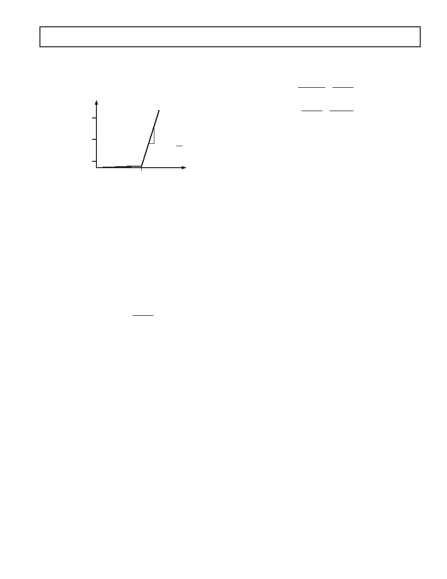
GENERAL
Laser diodes have current-in to light-out transfer functions as
shown in Figure 1. Two key characteristics of this transfer func-
tion are the threshold current, I
TH
, and slope in the linear region
beyond the threshold current, referred to as slope efficiency (LI).
P
I
LI =
P
I
I
TH
CURRENT
P
AV
OPTICAL PO
WER
Figure 1. Laser Transfer Function
CONTROL
A monitor photodiode (MPD) is required to control the laser
diode. The MPD current is fed into the ADN2830 to control
the power, continuously adjusting the bias current in response
to the laser's changing threshold current and light to current
(LI) slope (slope efficiency).
The ADN2830 uses automatic power control (APC) to maintain
a constant power over time and temperature.
The average power is controlled by the R
PSET
resistor
connected between the PSET pin and ground. The PSET pin
is kept 1.23 V above GND. For an initial setup, the R
PSET
resis-
tor can be calculated using the following formula.
R
V
I
PSET
AV
=
1 23
.
where I
AV
is average MPD current.
Note the I
PSET
will change from device to device. It is not
required to know exact values for LI and MPD optical coupling.
LOOP BANDWIDTH SELECTION
Capacitor values greater than 22 nF are used to set the actual
loop bandwidth. This capacitor is placed between the PAVCAP
pin and ground. It is important that the capacitor is a low leak-
age multilayer ceramic with an insulation resistance greater than
100 G
or a time constant of 1000 sec, whichever is less.
ALARMS
The ADN2830 has two active high alarms, DEGRADE and
FAIL. A resistor between ground and the ASET pin is used to
set the current at which these alarms are raised. The current
through the ASET resistor is a ratio of (N 200):1 to the FAIL
alarm threshold (N is the number of ADN2830s in parallel).
The DEGRADE alarm will be raised at 90% of this level.
Example:
I
mA N
I
mA
FAIL
DEGRADE
=
=
=
50
1
45
,
I
I
N
mA
A
ASET
BIASTRIP
=
◊
=
=
µ
200
50
200
250
*R
V
I
A
k
ASET
ASET
=
=
=
1 23
1 23
250
4 92
.
.
.
µ
The laser degrade alarm, DEGRADE, gives a warning of imminent
laser failure if the laser diode degrades further or environmental condi-
tions continue to stress the laser diode, e.g., increasing temperature.
The laser fail alarm, FAIL, is activated when:
∑
The ASET threshold is reached.
∑
The ALS pin is set high. This shuts off the modulation and
bias currents to the laser diode, resulting in the MPD current
dropping to zero.
DEGRADE will only be raised when the bias current exceeds
90% of the ASET current.
MONITOR CURRENTS
IBMON and IMPDMON are current controlled current sources
from V
CC
. They mirror the bias and MPD current for increased
monitoring functionality. An external resistor to GND gives a
voltage proportional to the current monitored. If the IMPDMON
function is not used, the IMPD pin must be grounded and the
monitor photodiode must be tied directly to the PSET pin.
AUTOMATIC LASER SHUTDOWN
When ALS is logic high, the bias current is turned off. Correct
operation of ALS can be confirmed by the fail alarm being
raised when ALS is asserted. Note that this is the only time
DEGRADE will be low while FAIL is high.
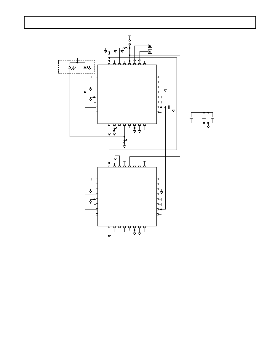
MODE
The MODE feature on the ADN2830 allows the user to operate
more than one ADN2830 in parallel current boosting mode to
achieve up to N 200 mA of bias current (N is the number of
ADN2830s in parallel). When using parallel boosting mode, one
device is run as the master, the other as the slave. The MODE
pin on the master is tied to ALS and the MODE pin on the
slave is tied high (see Figure 3 for reference circuit).
ALARM INTERFACES
The FAIL and DEGRADE outputs have an internal 30 k
pull-up resistor that is used to pull the digital high value to V
CC.
However, the alarm output may be overdriven with an external
resistor allowing the alarm interfacing to non-V
CC
levels.
Non-V
CC
alarm output levels must be below the V
CC
used for
the ADN2830.
*The smallest value for R
ASET
is 1.2 k
, as this corresponds to the IBIAS
maximum of N 200 mA.
REV. A
ADN2830
≠6≠
POWER CONSUMPTION
The ADN2830 die temperature must be kept below 125
∞C.
The exposed paddle should be connected in such a manner that
it is at the same potential as the ADN2830 ground pins. Power
consumption can be calculated using the following formulas.
T
T
P
DIE
AMBIENT
A
=
+
◊
J
I
I
CC
CCMIN
=
P
V
I
IBIAS
V
CC
CC
BIAS PIN
=
◊
+
◊
(
)
_
GND
ASET
NC
PSET
IMPD
IMPDMON
GND4
V
CC
4
NC
NC
GND1
NC
V
CC
5
V
CC
1
PAVCAP
PAVCAP
V
CC
2
NC
GND2
IBIAS
GND2
GND2
IBIAS
NC
IBMON
IBMON
GND3
V
CC
3
ALS
F
AIL
DEGRADE
MODE
1
8
16
24
32
NC = NO CONNECT
MPD
LD
V
CC
V
CC
FAIL
DEGRADE
1 F
100nF
10 F
V
CC
GND
PLACE 100nF CAP
CLOSE TO PIN 8
ADN2830
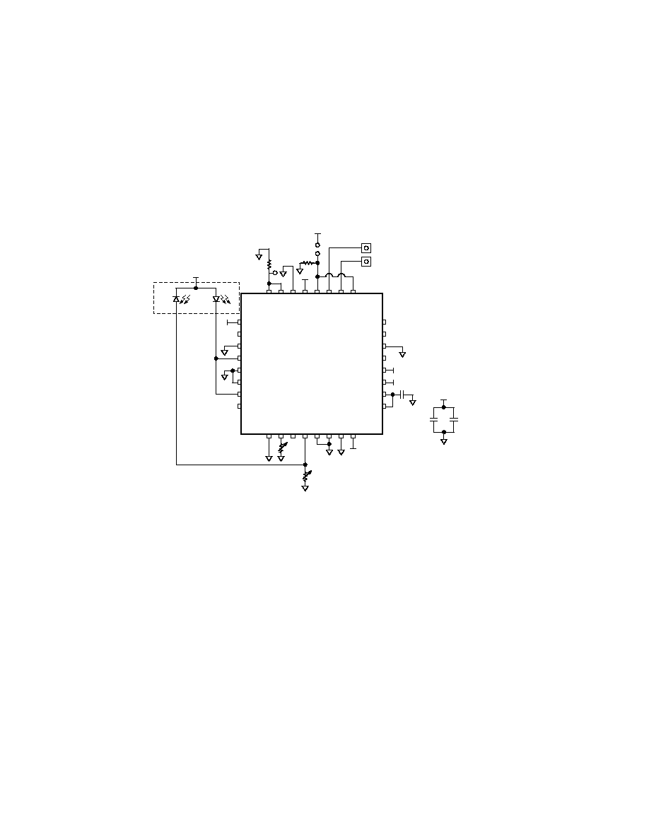
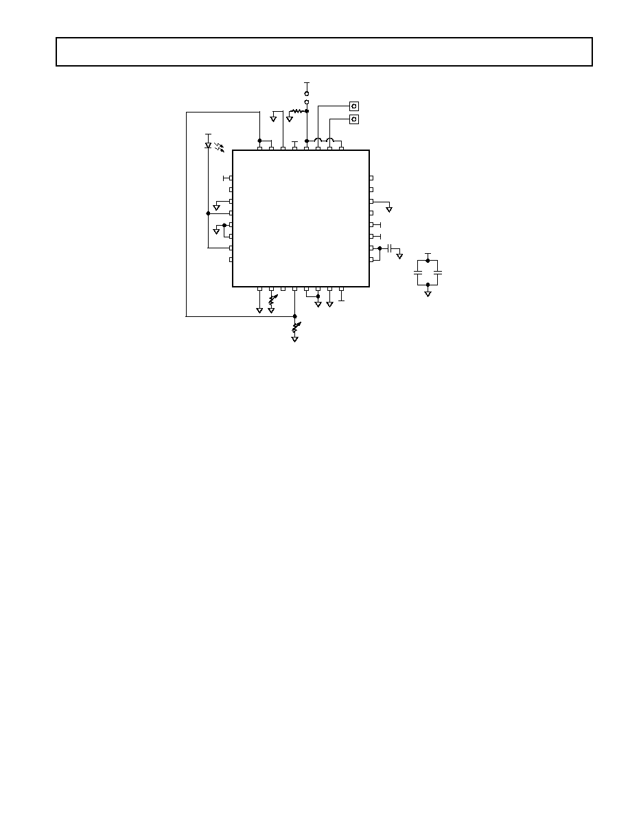
Figure 2. Test Circuit, Standalone Mode, IMPD Input Not Used
REV. A
ADN2830
≠7≠
GND
ASET
NC
PSET
IMPD
IMPDMON
GND4
V
CC
4
NC
NC
GND1
NC
V
CC
5
V
CC
1
PAVCAP
PAVCAP
V
CC
2
NC
GND2
IBIAS
GND2
GND2
IBIAS
NC
IBMON
IBMON
GND3
V
CC
3
ALS
F
AIL
DEGRADE
MODE
1
8
16
24
32
NC = NO CONNECT
MPD
LD
V
CC
V
CC
FAIL
DEGRADE
100nF
10 F
V
CC
GND
PLACE 100nF CAP
CLOSE TO PIN 8
100nF
GND
ASET
NC
PSET
IMPD
IMPDMON
GND4
V
CC
4
NC
NC
GND1
NC
V
CC
5
V
CC
1
PAVCAP
PAVCAP
V
CC
2
NC
GND2
IBIAS
GND2
GND2
IBIAS
NC
IBMON
IBMON
GND3
V
CC
3
ALS
F
AIL
DEGRADE
MODE
1
8
16
24
32
NC = NO CONNECT
ADN2830
ADN2830
Figure 3. Test Circuit, Second ADN2830 Used in Parallel Current Boosting Mode to Achieve 400 mA Max IBIAS
REV. A
ADN2830
≠8≠
GND
ASET
NC
PSET
IMPD
IMPDMON
GND4
V
CC
4
NC
NC
GND1
NC
V
CC
5
V
CC
1
PAVCAP
PAVCAP
V
CC
2
NC
GND2
IBIAS
GND2
GND2
IBIAS
NC
IBMON
IBMON
GND3
V
CC
3
ALS
F
AIL
DEGRADE
MODE
1
8
16
24
32
NC = NO CONNECT
MPD
LD
V
CC
V
CC
FAIL
DEGRADE
100nF
10 F
V
CC
GND
PLACE 100nF CAP
CLOSE TO PIN 8
ADN2830
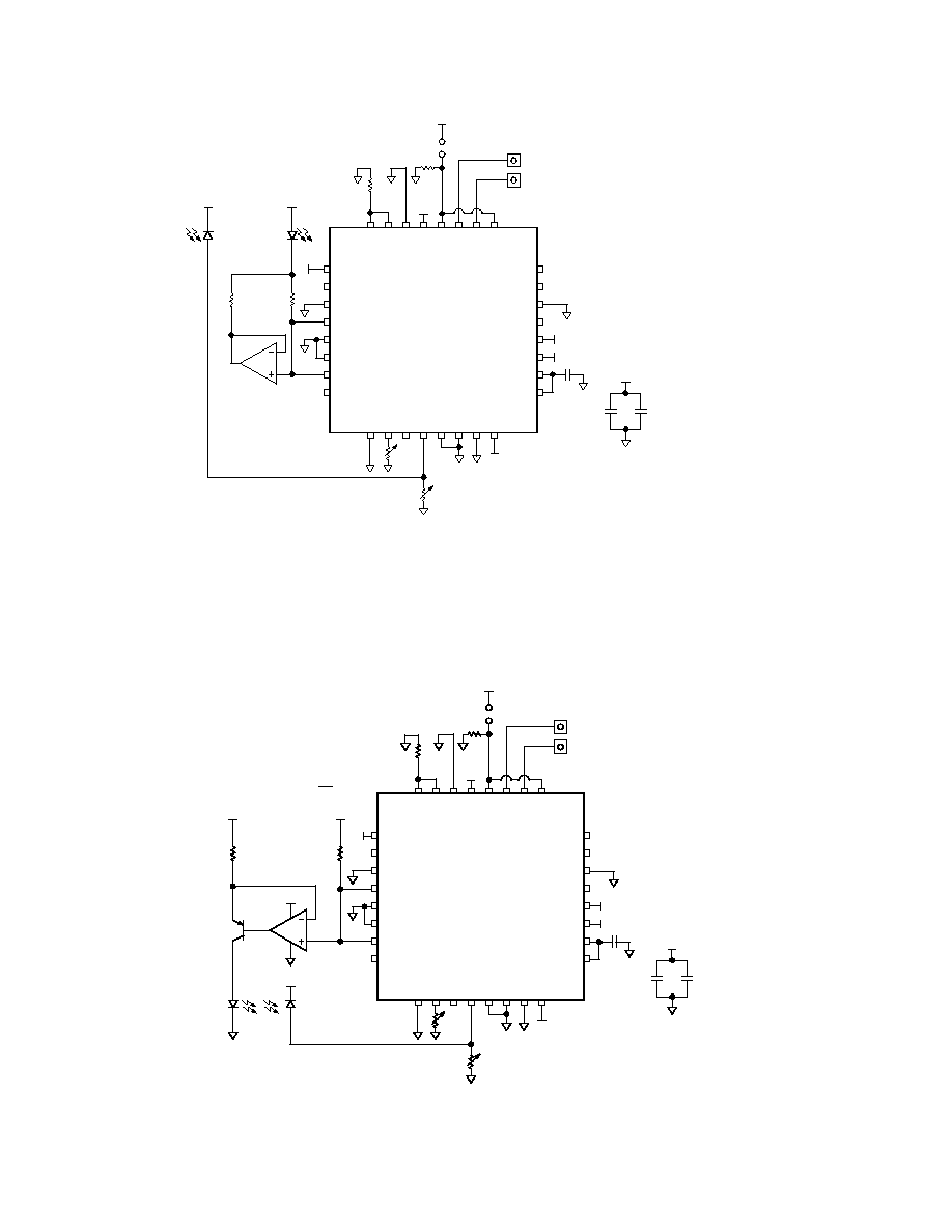
R1
R2
V
CC
NOTES
1.FOR DIGITAL CONTROL, REPLACE R
PSET
WITH A DIGITAL POTENTIOMETER FROM ANALOG DEVICES:
ADN2850 10-BIT RESOLUTION, 35 ppm/ C TC, EEPROM; AD5242 8-BIT RESOLUTION, 30 ppm/ C TC.
2.TOTAL CURRENT TO LASER = IBIAS + IBIAS
R1/R2.
3.FOR BEST ACCURACY, SIZE R1 TO HAVE A MAXIMUM VOLTAGE DROP ACROSS IT WITHIN THE HEADROOM
CONSTRAINTS.
4.FOR 250 mA EXTRA IBIAS (450 mA TOTAL) FROM AMP1, USE AD8591 AMPLIFIER. AMP1 IS THE OPERATIONAL AMPLIFIER
SHOWN IN THIS FIGURE.
5.FOR 350 mA EXTRA IBIAS (550 mA TOTAL) FROM AMP1, USE ANALOG DEVICES' SSM2211 AMPLIFIER. AMP1 IS THE
OPERATIONAL AMPLIFIER SHOWN IN THIS FIGURE.
Figure 4. The ADN2830 Configured with Current Multiplier
GND
ASET
NC
PSET
IMPD
IMPDMON
GND4
V
CC
4
NC
NC
GND1
NC
V
CC
5
V
CC
1
PAVCAP
PAVCAP
V
CC
2
NC
GND2
IBIAS
GND2
GND2
IBIAS
NC
IBMON
IBMON
GND3
V
CC
3
ALS
F
AIL
DEGRADE
MODE
1
8
16
24
32
NC = NO CONNECT
V
CC
V
CC
FAIL
DEGRADE
100nF
10 F
V
CC
GND
PLACE 100nF CAP
CLOSE TO PIN 8
ADN2830
R1
V
CC
AD820
MPD
V
CC
LD
V
CC
R2
CURRENT GAIN =
R1
R2
Figure 5. The ADN2830 Configured as Average Power Controller (Bias Current Sourced)
REV. A
ADN2830
≠9≠
GND
ASET
NC
PSET
IMPD
IMPDMON
GND4
V
CC
4
NC
NC
GND1
NC
V
CC
5
V
CC
1
PAVCAP
PAVCAP
V
CC
2
NC
GND2
IBIAS
GND2
GND2
IBIAS
NC
IBMON
IBMON
GND3
V
CC
3
ALS
F
AIL
DEGRADE
MODE
1
8
16
24
32
NC = NO CONNECT
V
CC
FAIL
DEGRADE
100nF
10 F
V
CC
GND
PLACE 100nF CAP
CLOSE TO PIN 8
ADN2830
LD
V
CC
Figure 6. The ADN2830 Configured as a Controlled Current
Source by Feeding Back the Bias Monitor Current to R
PSET
REV. A
ADN2830
≠10≠
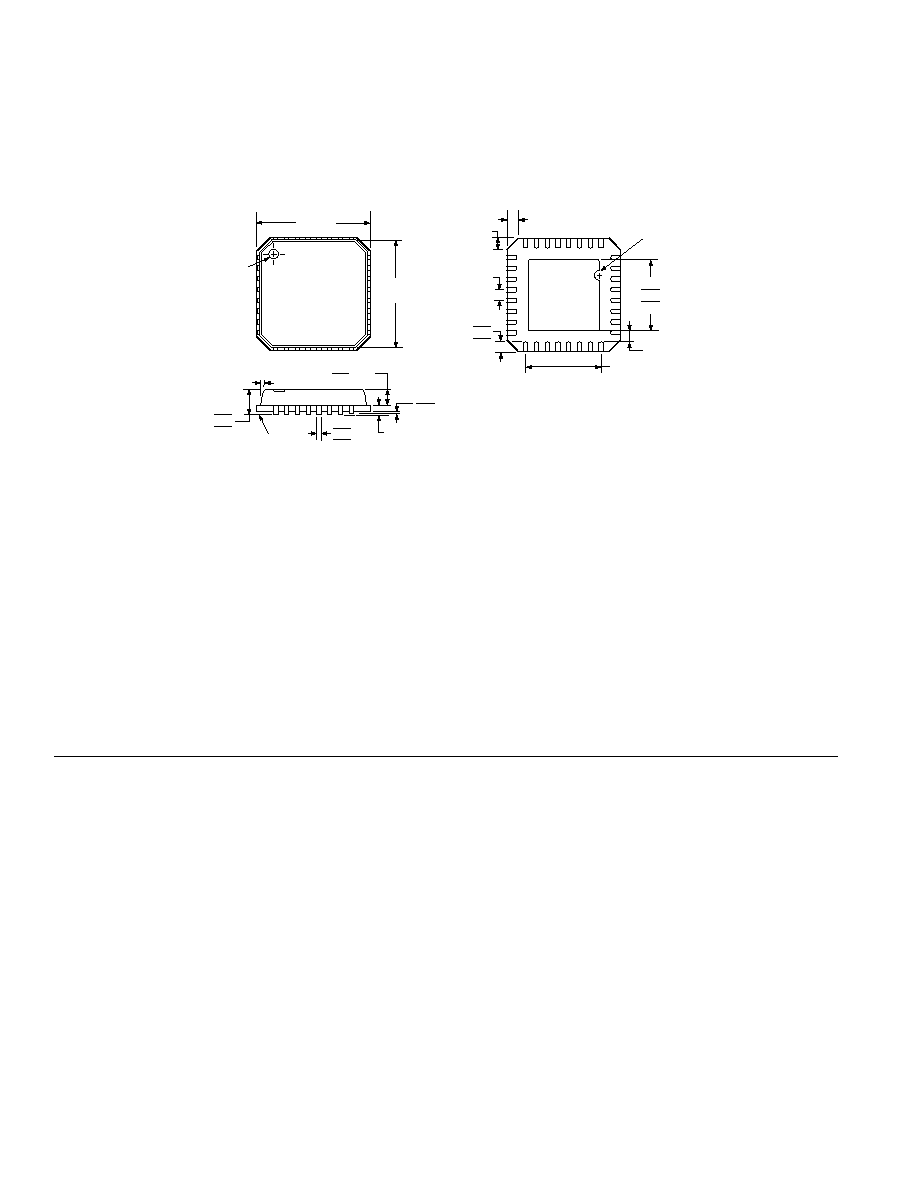
OUTLINE DIMENSIONS
32-Lead Frame Chip Scale Package [LFCSP]
(CP-32)
Dimensions shown in millimeters
COMPLIANT TO JEDEC STANDARDS MO-220-VHHD-2
0.30
0.23
0.18
0.20 REF
0.80 MAX
0.65 NOM
0.05 MAX
0.02 NOM
12
MAX
1.00
0.90
0.80
SEATING
PLANE
COPLANARITY
0.08
1
32
8
9
25
24
16
17
BOTTOM
VIEW
0.50
0.40
0.30
3.50 REF
0.50
BSC
PIN 1
INDICATOR
TOP
VIEW
5.00
BSC SQ
4.75
BSC SQ
SQ
3.25
3.10
2.95
PIN 1
INDICATOR
0.60 MAX
0.60 MAX
0.25 MIN
Revision History
Location
Page
6/03--Data Sheet changed from REV. 0 to REV. A.
Changes to ABSOLUTE MAXIMUM RATINGS . . . . . . . . . . . . . . . . . . . . . . . . . . . . . . . . . . . . . . . . . . . . . . . . . . . . . . . . . . . . . . 3
Updated OUTLINE DIMENSIONS . . . . . . . . . . . . . . . . . . . . . . . . . . . . . . . . . . . . . . . . . . . . . . . . . . . . . . . . . . . . . . . . . . . . . . . 10

≠11≠

≠12≠
C03020≠0≠6/03(A)