 | –≠–ª–µ–∫—Ç—Ä–æ–Ω–Ω—ã–π –∫–æ–º–ø–æ–Ω–µ–Ω—Ç: ADN2850 | –°–∫–∞—á–∞—Ç—å:  PDF PDF  ZIP ZIP |
Document Outline
- FEATURES
- APPLICATIONS
- GENERAL DESCRIPTION
- FUNCTIONAL BLOCK DIAGRAM
- SPECIFICATIONS
- TIMING DIAGRAMS
- ABSOLUTE MAXIMUM RATINGS
- ORDERING GUIDE
- PIN CONFIGURATIONS
- ADN2850BCP PIN FUNCTION DESCRIPTIONS
- ADN2850BRU PIN FUNCTION DESCRIPTIONS
- OPERATIONAL OVERVIEW
- OPERATION DETAIL
- Scratch Pad and EEMEM Programming
- EEMEM Protection
- Linear Increment and Decrement Commands
- Logarithmic Taper Mode Adjustment ( 6 dB/step)
- Using Additional Internal Nonvolatile EEMEM
- Calculating Actual Full-Scale Resistance
- Daisy-Chain Operation
- DIGITAL INPUT/OUTPUT CONFIGURATION
- SERIAL DATA INTERFACE
- TERMINAL VOLTAGE OPERATING RANGE
- Power-Up Sequence
- Layout and Power Supply Bypassing
- RDAC STRUCTURE
- CALCULATING THE PROGRAMMABLE RESISTANCE
- Typical Performance Characteristics
- PROGRAMMING EXAMPLES
- APPLICATIONS
- Optical Transmitter Calibration with ADN2841
- Incoming Optical Power Monitoring
- Resistance Scaling
- OUTLINE DIMENSIONS
- Revision History
REV. B
a
Information furnished by Analog Devices is believed to be accurate and
reliable. However, no responsibility is assumed by Analog Devices for its
use, nor for any infringements of patents or other rights of third parties that
may result from its use. No license is granted by implication or otherwise
under any patent or patent rights of Analog Devices.
One Technology Way, P.O. Box 9106, Norwood, MA 02062-9106, U.S.A.
Tel: 781/329-4700
www.analog.com
Fax: 781/326-8703
© Analog Devices, Inc., 2002
ADN2850
*
Nonvolatile Memory, Dual
1024-Position Programmable Resistors
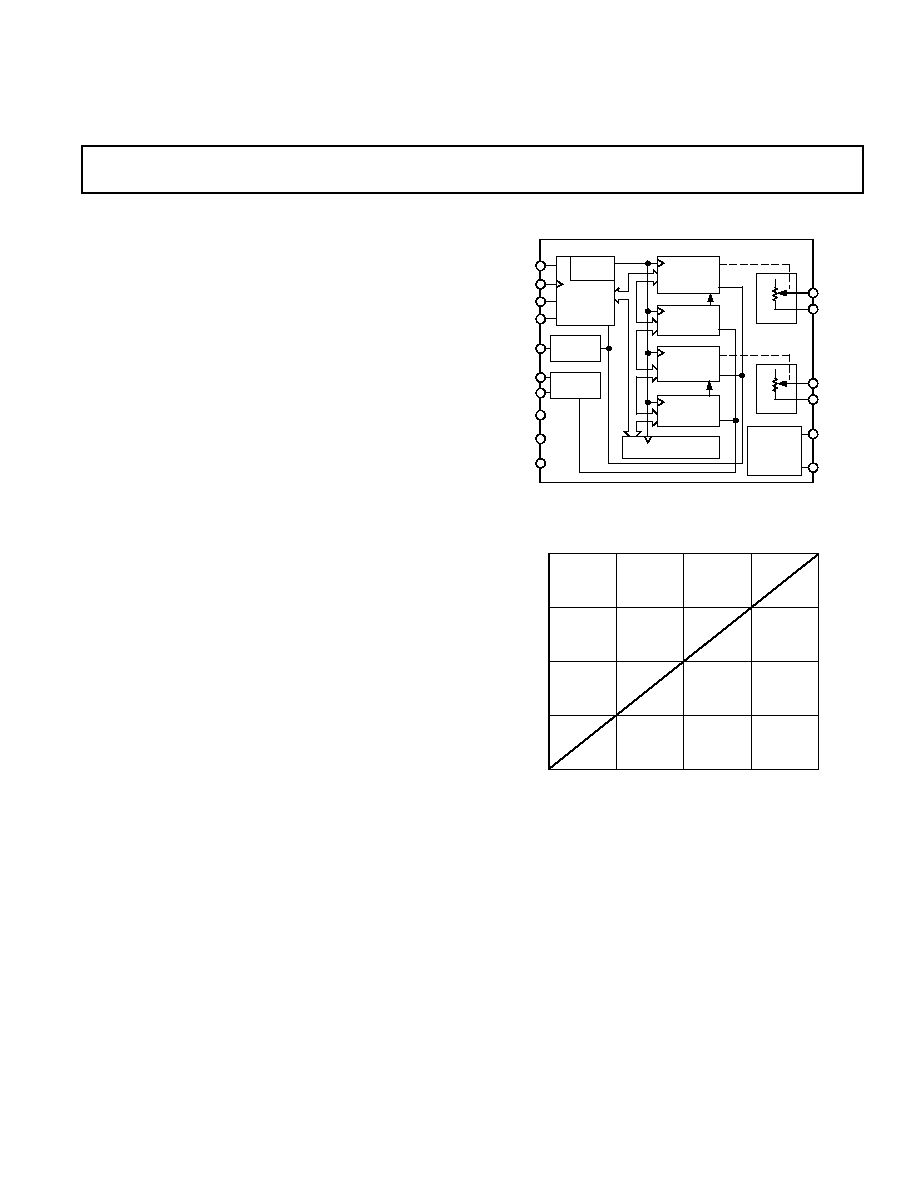
FUNCTIONAL BLOCK DIAGRAM
ADDR
DECODE
ADN2850
RDAC1
SERIAL
INTERFACE
CS
CLK
SDI
SDO
PR
WP
RDY
V
DD
V
SS
GND
RDAC1
REGISTER
EEMEM1
RDAC2
REGISTER
EEMEM2
26 BYTES
USER EEMEM
PWR ON
PRESET
EEMEM
CONTROL
W1
B1
RDAC2
W2
B2
CURRENT
MONITOR
I
1
I
2
V
1
V
2
CODE ≠ Decimal
100
75
0
0
1023
256
R
WB
(D) ≠ % of Full-Scale R
WB
512
768
50
25
Figure 1. R
WB
(D) vs. Decimal Code
FEATURES
Dual, 1024-Position Resolution
25 k , 250 k Full-Scale Resistance
Low Temperature Coefficient: 35 ppm/ C
Nonvolatile Memory
1
Preset Maintains Wiper Settings
Permanent Memory Write-Protection
Wiper Settings Read Back
Actual Tolerance Stored in EEMEM
1
Linear Increment/Decrement
Log Taper Increment/Decrement
SPI Compatible Serial Interface
3 V to 5 V Single Supply or 2.5 V Dual Supply
26 Bytes User Nonvolatile Memory for Constant Storage
Current Monitoring Configurable Function
100-Year Typical Data Retention T
A
= 55 C
APPLICATIONS
SONET, SDH, ATM, Gigabit Ethernet, DWDM Laser
Diode Driver Optical Supervisory Systems
GENERAL DESCRIPTION
The ADN2850 provides dual-channel, digitally controlled program-
mable resistors
2
with resolution of 1024 positions. These devices
perform the same electronic adjustment function as a mechanical
rheostat with enhanced resolution, solid-state reliability, and
superior low temperature coefficient performance. The ADN2850's
versatile programming via a standard serial interface allows
16 modes of operation and adjustment, including scratch pad pro-
gramming, memory storing and retrieving, increment/decrement,
log taper adjustment, wiper setting readback, and extra user
defined EEMEM
1
.
Another key feature of the ADN2850 is that the actual tolerance
is stored in the EEMEM. The actual full-scale resistance can
therefore be known, which is valuable for tolerance matching
and calibration.
In the scratch pad programming mode, a specific setting can be
programmed directly to the RDAC
2
register, which sets the resis-
tance between terminals W and B. The RDAC register can also
be loaded with a value previously stored in the EEMEM register.
The value in the EEMEM can be changed or protected. When
changes are made to the RDAC register, the value of the new
setting can be saved into the EEMEM. Thereafter, such value will
be transferred automatically to the RDAC register during system
power ON, which is enabled by the internal preset strobe.
EEMEM can also be retrieved through direct programming and
external preset pin control.
The linear step increment and decrement commands enable the
setting in the RDAC register to be moved UP or DOWN, one step
at a time. For logarithmic changes in wiper setting, a left/right
bit shift command adjusts the level in
±6 dB steps.
The ADN2850 is available in the 5 mm 5 mm 16-lead frame chip
scale LFCSP and thin 16-lead TSSOP packages. All parts are
guaranteed to operate over the extended industrial temperature
range of ≠40
∞C to +85∞C.
*Patent pending
NOTES
1
The term nonvolatile memory and EEMEM are used interchangeably.
2
The term programmable resistor and RDAC are used interchangeably.

REV. B
≠2≠
ADN2850≠SPECIFICATIONS
ELECTRICAL CHARACTERISTICS 25 k , 250 k VERSIONS
Parameter
Symbol
Conditions
Min
Typ
2
Max
Unit
DC CHARACTERISTICS RHEOSTAT MODE (Specifications apply to all RDACs)
Resistor Differential Nonlinearity
3
R-DNL
R
WB
≠2
+2
LSB
Resistor Integral Nonlinearity
3
R-INL
R
WB
≠4
+4
LSB
Resistance Temperature Coefficient
R
WB
/
T
35
ppm/
∞C
Wiper Resistance
R
W
V
DD
= 5 V, I
W
= 100
µA,
Code = Half-scale
50
100
V
DD
= 3 V, I
W
= 100
µA,
Code = Half-scale
200
Channel Resistance Matching
R
WB
/R
WB
Ch 1 and 2 R
WB
, Dx = 3FF
H
0.1
%
Nominal Resistor Tolerance
R
WB
≠30
+30
%
RESISTOR TERMINALS
Terminal Voltage Range
4
V
W, B
V
SS
V
DD
V
Capacitance
5
Bx
C
B
f = 1 MHz, measured to GND,
Code = Half-scale
11
pF
Capacitance
5
Wx
C
W
f = 1 MHz, measured to GND,
Code = Half-scale
80
pF
Common-Mode Leakage Current
6
I
CM
V
W
= V
B
= V
DD
/2
0.01
±2
µA
DIGITAL INPUTS AND OUTPUTS
Input Logic High
V
IH
With respect to GND, V
DD
= 5 V
2.4
V
Input Logic Low
V
IL
With respect to GND, V
DD
= 5 V
0.8
V
Input Logic High
V
IH
With respect to GND, V
DD
= 3 V
2.1
V
Input Logic Low
V
IL
With respect to GND, V
DD
= 3 V
0.6
V
Input Logic High
V
IH
With respect to GND,
V
DD
= +2.5 V, V
SS
= ≠2.5 V
2.0
V
Input Logic Low
V
IL
With respect to GND,
V
DD
= +2.5 V, V
SS
= ≠2.5 V
0.5
V
Output Logic High (SDO, RDY)
V
OH
R
PULL-UP
= 2.2 k
to 5 V
4.9
V
Output Logic Low
V
OL
I
OL
= 1.6 mA, V
LOGIC
= 5 V
0.4
V
Input Current
I
IL
V
IN
= 0 V or V
DD
±2.25
µA
Input Capacitance
5
C
IL
5
pF
POWER SUPPLIES
Single-Supply Power Range
V
DD
V
SS
= 0 V
3.0
5.5
V
Dual-Supply Power Range
V
DD
/V
SS
±2.25
±2.75
V
Positive Supply Current
I
DD
V
IH
= V
DD
or V
IL
= GND,
T
A
= 25
o
C
2
4.5
µA
Positive Supply Current
I
DD
V
IH
= V
DD
or V
IL
= GND
3.5
6.0
µA
Programming Mode Current
I
DD(PG)
V
IH
= V
DD
or V
IL
= GND
35
mA
Read Mode Current
7
I
DD(XFR)
V
IH
= V
DD
or V
IL
= GND
0.3
3
9
mA
Negative Supply Current
I
SS
V
IH
= V
DD
or V
IL
= GND,
V
DD
= +2.5 V, V
SS
= ≠2.5 V
3.5
6.0
µA
Power Dissipation
8
P
DISS
V
IH
= V
DD
or V
IL
= GND
18
50
µW
Power Supply Sensitivity
P
SS
V
DD
= 5 V
± 10%
0.002
0.01
%/%
CURRENT MONITOR TERMINALS
Current Sink at V
1
9
I
1
0.0001
10
mA
Current Sink at V
2
I
2
10
mA
DYNAMIC CHARACTERISTICS
5, 10
Resistor Noise Spectral Density
e
N_WB
R
WB_FS
= 25 k
/250 k, f = 1 kHz
20/64
nV/
Hz
Analog Crosstalk (C
W1
/C
W2
)
C
T
V
B1
= V
B2
= 0 V, Measured V
W1
with
V
W2
= 100 mV p-p @ f = 100 kHz,
Code
1
= Code 2 = 200
H
≠65
dB
(V
DD
= 3 V to 5.5 V and ≠40 C < T
A
< +85 C,
unless otherwise noted.)
1

REV. B
ADN2850
≠3≠
Parameter
Symbol
Conditions
Min
Typ
2
Max
Unit
INTERFACE TIMING CHARACTERISTICS (apply to all parts)
5, 11
Clock Cycle Time (t
CYC
)
t
1
20
ns
CS Setup Time
t
2
10
ns
CLK Shutdown Time to
CS Rise
t
3
1
t
CYC
Input Clock Pulsewidth
t
4
, t
5
Clock Level High or Low
10
ns
Data Setup Time
t
6
From Positive CLK Transition
5
ns
Data Hold Time
t
7
From Positive CLK Transition
5
ns
CS to SDO ≠ SPI Line Acquire
t
8
40
ns
CS to SDO ≠ SPI Line Release
t
9
50
ns
CLK to SDO Propagation Delay
12
t
10
R
P
= 2.2 k
, C
L
< 20 pF
50
ns
CS High Pulsewidth
13
t
12
10
ns
CS High to CS High
13
t
13
4
t
CYC
RDY Rise to
CS Fall
t
14
0
ns
CS Rise to RDY Fall Time
t
15
0.15
0.3
ms
Read/Store to Nonvolatile EEMEM
14
t
16
Applies to Command 2
H
, 3
H
, 9
H
35
ms
CS Rise to Clock Edge Setup
t
17
10
ns
Preset Pulsewidth (Asynchronous)
t
PRW
Not Shown in Timing Diagram
50
ns
Preset Response Time to Wiper Setting
t
PRESP
PR Pulsed Low to Refresh
140
µs
Wiper Positions
FLASH/EE MEMORY RELIABILITY
Endurance
15
100
K Cycles
Data Retention
16
100
Years
NOTES
1
Parts can be operated at 2.7 V single supply, except from 08C to ≠408C, where minimum 3 V is needed.
2
Typicals represent average readings at 258C and V
DD
= 5 V.
3
Resistor position nonlinearity error R-INL is the deviation from an ideal value measured between the maximum resistance and the minimum resistance wiper positions.
R-DNL measures the relative step change from ideal between successive tap positions. I
W
~ 50
µA for V
DD
= 2.7 V and I
W
~ 400
µA for V
DD
= 5 V.
4
Resistor terminals W and B have no limitations on polarity with respect to each other.
5
Guaranteed by design and not subject to production test.
6
Common-mode leakage current is a measure of the dc leakage from any terminal B and W to a common-mode bias level of V
DD
/2.
7
Transfer (XFR) mode current is not continuous. Current consumed while EEMEM locations are read and transferred to the RDAC register. See TPC 9.
8
P
DISS
is calculated from (I
DD
V
DD
) + (I
SS
V
SS
).
9
Applies to photodiode of optical receiver.
10
All dynamic characteristics use V
DD
= +2.5 V and V
SS
= ≠2.5 V.
11
See timing diagram for location of measured values. All input control voltages are specified with t
R
= t
F
= 2.5 ns (10% to 90% of 3 V) and timed from a voltage level of 1.5 V.
Switching characteristics are measured using both V
DD
= 3 V and 5 V.
12
Propagation delay depends on value of V
DD
, R
PULL_UP
, and C
L
. See Applications section.
13
Valid for commands that do not activate the RDY pin.
14
RDY pin low only for commands 2, 3, 8, 9, 10, and PR hardware pulse: CMD_8 ~ 1 ms; CMD_9, 10 ~ 0.1 ms; CMD_2, 3 ~ 20 ms. Device operation at T
A
= ≠40
∞C
and V
DD
< 3 V extends the save time to 35 ms.
15
Endurance is qualified to 100,000 cycles as per JEDEC Std. 22 method A117 and measured at ≠40
∞C, +25∞C, and +85∞C; typical endurance at +25∞C is 700,000 cycles.
16
Retention lifetime equivalent at junction temperature (T
J
) = 55
∞C as per JEDEC Std. 22, Method A117. Retention lifetime based on an activation energy of 0.6 V will
derate with junction temperature.
Specifications subject to change without notice.
The ADN2850 contains 16,000 transistors. Die size: 93 mil 103 mil, 10,197 sq mil.

REV. B
≠4≠
ADN2850
TIMING DIAGRAMS
CPOL = 1
t
12
t
13
t
3
t
17
t
9
t
11
t
5
t
4
t
2
t
1
CLK
t
8
*
MSB
LSB OUT
MSB
LSB
RDY
CPHA = 1
t
10
t
7
t
6
t
14
t
15
t
16
*NOT DEFINED, BUT NORMALLY LSB OF CHARACTER PREVIOUSLY TRANSMITTED.
THE CPOL = 1 MICROCONTROLLER COMMAND ALIGNS THE INCOMING DATA TO THE POSITIVE EDGE OF THE CLOCK.
CS
SDO
SDI
Figure 2a. CPHA = 1 Timing Diagram
t
12
t
13
t
3
t
17
t
9
t
5
t
4
t
2
t
1
CLK
CPOL = 0
t
8
MSB OUT
LSB
SDO
MSB IN
LSB
SDI
RDY
CPHA = 0
t
10
t
7
t
6
t
14
t
15
t
16
*NOT DEFINED, BUT NORMALLY MSB OF CHARACTER JUST RECEIVED.
THE CPOL = 0 MICROCONTROLLER COMMAND ALIGNS THE INCOMING DATA TO THE POSITIVE EDGE OF THE CLOCK.
*
CS
t
11
Figure 2b. CPHA = 0 Timing Diagram

REV. B
ADN2850
≠5≠
ABSOLUTE MAXIMUM RATINGS
1
(T
A
= 25
∞C, unless otherwise noted.)
V
DD
to GND . . . . . . . . . . . . . . . . . . . . . . . . . . . ≠0.3 V, +7 V
V
SS
to GND . . . . . . . . . . . . . . . . . . . . . . . . . . . . +0.3 V, ≠7 V
V
DD
to V
SS
. . . . . . . . . . . . . . . . . . . . . . . . . . . . . . . . . . . . . 7 V
V
B
, V
W
to GND . . . . . . . . . . . . . . . . V
SS
≠ 0.3 V, V
DD
+ 0.3 V
I
B
, I
W
Intermittent
2
. . . . . . . . . . . . . . . . . . . . . . . . . . . . . .
±20 mA
Continuous . . . . . . . . . . . . . . . . . . . . . . . . . . . . . . .
±2 mA
Digital Inputs and Output Voltage
to GND . . . . . . . . . . . . . . . . . . . . . . . . ≠0.3 V, V
DD
+ 0.3 V
Operating Temperature Range
3
. . . . . . . . . . . ≠40
∞C to +85∞C
Maximum Junction Temperature (T
J MAX
) . . . . . . . . . 150
∞C
Storage Temperature . . . . . . . . . . . . . . . . . . ≠65
∞C to +150∞C
Lead Temperature, Soldering
4
Vapor Phase (60 sec) . . . . . . . . . . . . . . . . . . . . . . . . . 215 C
Infrared (15 sec) . . . . . . . . . . . . . . . . . . . . . . . . . . . . 220 C
Thermal Resistance Junction-to-Ambient
JA,
LFCSP-16 . . . . . . . . . . . . . . . . . . . . . . . . . . . . . . . 35
∞C/W
TSSOP-16 . . . . . . . . . . . . . . . . . . . . . . . . . . . . . . 150
∞C/W
Thermal Resistance Junction-to-Case
JC,
TSSOP-16 . . . . . . . . . . . . . . . . . . . . . . . . . . . . . . . 28
∞C/W
Package Power Dissipation = (T
J MAX
≠ T
A
)/
JA
NOTES
1
Stresses above those listed under Absolute Maximum Ratings may cause perma-
nent damage to the device. This is a stress rating; functional operation of the device
at these or any other conditions above those listed in the operational sections of this
specification is not implied. Exposure to absolute maximum rating conditions for
extended periods may affect device reliability.
2
Maximum terminal current is bounded by the maximum current handling of the
switches, maximum power dissipation of the package, and maximum applied
voltage across any two of the B and W terminals at a given resistance.
3
Includes programming of nonvolatile memory.
4
Applicable to TSSOP-16 only. For LFCSP-16, please consult factory for details.
CAUTION
ESD (electrostatic discharge) sensitive device. Electrostatic charges as high as 4000 V readily
accumulate on the human body and test equipment and can discharge without detection. Although
the ADN2850 features proprietary ESD protection circuitry, permanent damage may occur on
devices subjected to high energy electrostatic discharges. Therefore, proper ESD precautions are
recommended to avoid performance degradation or loss of functionality.
WARNING!
ESD SENSITIVE DEVICE
ORDERING GUIDE
R
WB_FS
RDNL RINL
Temperature
Package
Package
Ordering
Model
(k )
(LSB)
(LSB)
Range (
∞C)
Description
Option
Quantity
Top Mark
*
ADN2850BCP25
25
±2
±4
≠40 to +85
LFCSP-16
CP-16
96
BCP25
ADN2850BCP25-RL7
25
±2
±4
≠40 to +85
LFCSP-16
CP-16
1,000
BCP25
7
" Reel
ADN2850BCP250
250
±2
±4
≠40 to +85
LFCSP-16
CP-16
96
BCP250
ADN2850BCP250-RL7
250
±2
±4
≠40 to +85
LFCSP-16
CP-16
1,000
BCP250
7
" Reel
ADN2850BRU25
25
±2
±4
≠40 to +85
TSSOP-16
RU-16
96
2850B25
ADN2850BRU25-RL7
25
±2
±4
≠40 to +85
TSSOP-16
RU-16
1,000
2850B25
7
" Reel
*Line 1 contains product number, ADN2850, line 2 Top Mark branding contains differentiating detail by part type, line 3 contains lot number, line 4 contains product
date code YYWW.
REV. B
≠6≠
ADN2850
V
SS
GND
V
1
V
2
PR
WP
V
DD
16
CS
RD
Y
CLK
SDI
W2
B2
B1
W1
ADN2850BCP
CHIP SCALE
PACKAGE
15 14
13
12
11
10
9
8
7
6
5
SDO
4
3
2
1
ADN2850BCP PIN FUNCTION DESCRIPTIONS
Pin
No.
Mnemonic Description
1
SDO
Serial Data Output Pin. Open-Drain output
requires external pull-up resistor. CMD_9 and
CMD_10 activate the SDO output. See
Instruction Operation Truth Table (Table II).
Other commands shift out the previously
loaded SDI bit pattern delayed by 24 clock
pulses. This allows daisy-chain operation of
multiple packages.
2
GND
Ground Pin, logic ground reference
3
V
SS
Negative Supply. Connect to zero volts for
single-supply applications.
4
V
1
Log Output Voltage 1 generated from internal
diode configured transistor
5
W1
Wiper terminal of RDAC1 ADDR
(RDAC1) = 0
H
.
6
B1
B terminal of RDAC1
7
B2
B terminal of RDAC2
8
W2
Wiper terminal of RDAC2. ADDR
(RDAC2) = 1
H
.
9
V
2
Log Output Voltage 2 generated from internal
diode configured transistor
10
V
DD
Positive Power Supply Pin
11
WP
Write Protect Pin. When active low,
WP
prevents any changes to the present register
contents, except
PR and CMD_1 and CMD_8
will refresh the RDAC register from EEMEM.
Execute a NOP instruction before returning
to
WP high.
12
PR
Hardware Override Preset Pin. Refreshes the
scratch pad register with current contents of
the EEMEM register. Factory default loads
midscale 512
10
until EEMEM loaded with
a new value by the user (
PR is activated at
the logic high transition).
13
CS
Serial Register chip select active low.
Serial register operation takes place when
CS returns to logic high.
14
RDY
Ready. Active high open-drain output. Identifies
completion of commands 2, 3, 8, 9, 10, and
PR.
15
CLK
Serial Input Register Clock Pin. Shifts in
one bit at a time on positive clock edges.
16
SDI
Serial Data Input Pin. Shifts in one bit at a time
on positive clock CLK edges. MSB loaded first.
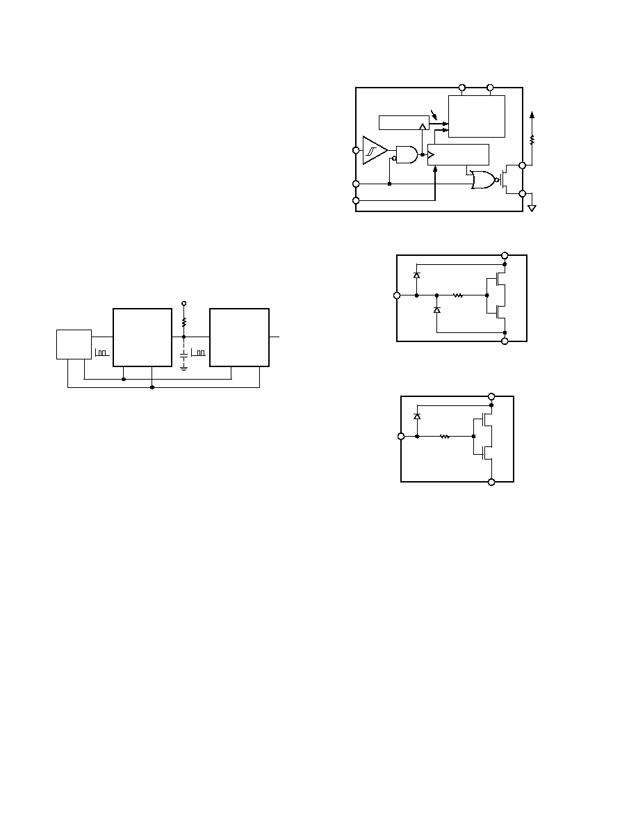
TOP VIEW
(Not To Scale)
1
2
3
4
5
6
7
8
SDI
SDO
GND
V
1
V
SS
W1
ADN2850BRU
CLK
B1
16
15
14
13
12
11
10
9
CS
PR
WP
V
DD
V
2
W2
B2
RDY
ADN2850BRU PIN FUNCTION DESCRIPTIONS
Pin
No.
Mnemonic Description
1
CLK
Serial Input Register Clock Pin. Shifts in
one bit at a time on positive clock edges.
2
SDI
Serial Data Input Pin. Shifts in one bit at
a time on positive clock CLK edges.
MSB loaded first.
3
SDO
Serial Data Output Pin. Open-drain out put
requires external pull-up resistor. CMD_9
and CMD_10 activate the SDO output. See
Instruction Operation Truth Table (Table II).
Other commands shift out the previously
loaded SDI bit pattern delayed by 24 clock
pulses. This allows daisy-chain operation of
multiple packages.
4
GND
Ground Pin, logic ground reference
5
V
SS
Negative Supply. Connect to zero volts for
single-supply applications.
6
V
1
Log Output Voltage 1 generated from internal
diode configured transistor
7
W1
Wiper terminal of RDAC1. ADDR
(RDAC1) = 0
H
.
8
B1
B terminal of RDAC1
9
B2
B terminal of RDAC2
10
W2
Wiper terminal of RDAC2. ADDR
(RDAC2) = 1
H
.
11
V
2
Log Output Voltage 2 generated from internal
diode configured transistor
12
V
DD
Positive Power Supply Pin
13
WP
Write Protect Pin. When active low,
WP prevents
any changes to the present contents except
PR
and CMD_1 and CMD_8 will refresh the
RDAC register from EEMEM. Execute a NOP
instruction before returning to
WP high.
14
PR
Hardware Override Preset Pin. Refreshes the
scratch pad register with current contents of
the EEMEM register. Factory default loads
midscale 512
10
until EEMEM loaded with a
new value by the user (
PR is activated at the
logic high transition).
15
CS
Serial Register chip select active low. Serial
register operation takes place when
CS returns
to logic high.
16
RDY
Ready. Active high open-drain output. Identifies
completion of commands 2, 3, 8, 9, 10, and
PR.
PIN CONFIGURATIONS

REV. B
ADN2850
≠7≠
Table I. 24-Bit Serial Data-Word
MSB
Instruction Byte 0
Data Byte 1
Data Byte 0
LSB
RDAC
C3
C2
C1 C0
0
0
0
A0
X
X
X
X
X
X
D9 D8 D7 D6 D5 D4 D3 D2 D1 D0
EEMEM C3
C2
C1 C0
A3
A2
A1 A0
D15 D14 D13 D12 D11 D10 D9 D8 D7 D6 D5 D4 D3 D2 D1 D0
Command bits are C0 to C3. Address bits are A3≠A0. Data bits D0 to D9 are applicable to RDAC wiper register whereas D0 to D15 are applicable to EEMEM
Register. Command instruction codes are defined in Table II.
Table II. Instruction Operation Truth Table
1, 2, 3
Inst
Instruction Byte 0
Data Byte 1
Data Byte 0
Operation
Number
B23 ∑ ∑ ∑ ∑ ∑ ∑ ∑ ∑ ∑ ∑ ∑ ∑ ∑ ∑ ∑ ∑ B16 B15 ∑ ∑ ∑ ∑ ∑ ∑ B8
B7 ∑ ∑ ∑ ∑ ∑ B0
C3 C2 C1 C0 A3 A2 A1 A0
X ∑ ∑ ∑ ∑ D9 D8
D7 ∑ ∑ ∑ ∑ ∑ D0
0
0
0
0
0
X X X
X
X ∑ ∑ ∑ ∑ X X
X ∑ ∑ ∑ ∑ ∑ ∑ X
NOP: Do nothing. See Table XI for Programming
example.
1
0
0
0
1
0
0
0
A0
X ∑ ∑ ∑ ∑ X X
X ∑ ∑ ∑ ∑ ∑ ∑ X
Retrieve contents of EEMEM(A0) to RDAC(A0)
Register. This command leaves device in the Read
Program power state. To return part to the idle state,
perform NOP instruction 0. See Table XI.
2
0
0
1
0
0
0
0
A0
X ∑ ∑ ∑ ∑ X X
X ∑ ∑ ∑ ∑ ∑ ∑ X
SAVE WIPER SETTING: Write contents of RDAC(A0)
to EEMEM(A0). See Table X.
3
4
0
0
1
1
A3 A2 A1 A0
D15 ∑ ∑ ∑ ∑ D8
D7 ∑ ∑ ∑ ∑ ∑ D0 Write contents of Serial Register Data Bytes 0 and
1 (total 16-bit) to EEMEM(ADDR). See Table XIII.
4
5
0
1
0
0
0
0
0
A0
X ∑ ∑ ∑ ∑ X X
X ∑ ∑ ∑ ∑ ∑ ∑ X
Decrement 6 dB: Right shift contents of RDAC(A0)
Register, stops at all "Zeros."
5
5
0
1
0
1
X X X
X
X ∑ ∑ ∑ ∑ X X
X ∑ ∑ ∑ ∑ ∑ ∑ X
Decrement All 6 dB: Right shift contents of all RDAC
Registers, stops at all "Zeros."
6
5
0
1
1
0
0
0
0
A0
X ∑ ∑ ∑ ∑ X X
X ∑ ∑ ∑ ∑ ∑ ∑ X
Decrement contents of RDAC(A0) by "One," stops
at all "Zeros."
7
5
0
1
1
1
X X X
X
X ∑ ∑ ∑ ∑ X X
X ∑ ∑ ∑ ∑ ∑ ∑ X
Decrement contents of all RDAC Registers by
"One," stops at all "Zeros."
8
1
0
0
0
X X X
X
X ∑ ∑ ∑ ∑ X X
X ∑ ∑ ∑ ∑ ∑ ∑ X
RESET: Load all RDACs with their corresponding
EEMEM previously saved values.
9
1
0
0
1
A3 A2 A1 A0
X ∑ ∑ ∑ ∑ X X
X ∑ ∑ ∑ ∑ ∑ ∑ X
Transfer contents of EEMEM (ADDR) to Serial
Register Data Bytes 0 and 1, and previously stored
data can be read out from the SDO pin. See Table XIV.
10
1
0
1
0
0
0
0
A0
X ∑ ∑ ∑ ∑ X X
X ∑ ∑ ∑ ∑ ∑ ∑ X
Transfer contents of RDAC (A0) to Serial Register
Data Bytes 0 and 1, and wiper setting can be read
from the SDO pin. See Table XV.
11
1
0
1
1
0
0
0
A0
X ∑ ∑ ∑ ∑ D9 D8
D7 ∑ ∑ ∑ ∑ ∑ D0 Write contents of Serial Register Data Bytes 0 and
1 (total 11-bit) to RDAC(A0). See Table IX.
12
5
1
1
0
0
0
0
0
A0
X ∑ ∑ ∑ ∑ X X
X ∑ ∑ ∑ ∑ ∑ ∑ X
Increment 6 dB: Left shift contents of RDAC(A0),
stops at all "Ones." See Table XII.
13
5
1
1
0
1
X X X
X
X ∑ ∑ ∑ ∑ X X
X ∑ ∑ ∑ ∑ ∑ ∑ X
Increment All 6 dB: Left shift contents of all RDAC
Registers, stops at all "Ones."
14
5
1
1
1
0
0
0
0
A0
X ∑ ∑ ∑ ∑ X X
X ∑ ∑ ∑ ∑ ∑ ∑ X
Increment contents of RDAC(A0) by "One," stops
at all "Ones." See Table X.
15
5
1
1
1
1
X X X
X
X ∑ ∑ ∑ ∑ X X
X ∑ ∑ ∑ ∑ ∑ ∑ X
Increment contents of all RDAC Registers by "One,"
stops at all "Ones."
NOTES
1
The SDO output shifts out the last 24 bits of data clocked into the serial register for daisy-chain operation. Exception: for any instruction following Instruction 9 or 10,
the selected internal register data will be present in data byte 0 and 1. The instructions following 9 and 10 must also be a full 24-bit data-word to completely clock out
the contents of the serial register.
2
The RDAC register is a volatile scratch pad register that is refreshed at power ON from the corresponding nonvolatile EEMEM register.
3
Execution of the above operations takes place when the
CS strobe returns to logic high.
4
Instruction 3 writes 2 data bytes (total 16-bit) to EEMEM. But in the cases of addresses 0 and 1, only the last 10 bits are valid for wiper position setting.
5
The increment, decrement, and shift commands ignore the contents of the shift register data bytes 0 and 1.

REV. B
≠8≠
ADN2850
OPERATIONAL OVERVIEW
The ADN2850 programmable resistor is designed to operate as
a true variable resistor. The resistor wiper position is determined
by the RDAC register contents. The RDAC register acts as a
scratch pad register which allows unlimited changes of resistance
settings. The scratch pad register can be programmed with any
position setting using the standard SPI serial interface by loading
the 24-bit data-word. The format of the data-word is that the first
4 bits are instructions, the following 4 bits are addresses, and the
last 16 bits are data. Once a specific value is set, this value can be
saved into a corresponding EEMEM register. During subsequent
power-ups, the wiper setting will automatically be loaded at that
value. Saving data to the EEMEM takes about 25 ms and con-
sumes approximately 20 mA. During this time the shift register
is locked, preventing any changes from taking place. The RDY pin
indicates the completion of this EEMEM saving process. There
are also 13 two-bytes addresses, of user defined data that can be
stored in EEMEM.
OPERATION DETAIL
There are 16 instructions that facilitate users' programming
needs. Referring to Table II, the instructions are:
0. Do Nothing
1. Restore EEMEM setting to RDAC
2. Save RDAC setting to EEMEM
3. Save user data or RDAC setting to EEMEM
4. Decrement 6 dB
5. Decrement all 6 dB
6. Decrement one step
7. Decrement all one step
8. Reset all EEMEM settings to RDAC
9. Read EEMEM to SDO
10. Read Wiper Setting to SDO
11. Write data to RDAC
12. Increment 6 dB
13. Increment all 6 dB
14. Increment one step
15. Increment all one step
Tables VIII to XIV provide a few programming examples by using
some of these instructions.
Scratch Pad and EEMEM Programming
The basic mode of setting the programmable resistor wiper position
(programming the scratch pad register) is done by loading the
serial data input register with the instruction 11, the corresponding
address, and the data. Since the scratch pad register is a standard
logic register, there is no restriction on the number of changes
allowed. When the desired wiper position is determined, the user can
load the serial data input register with the instruction 2, which stores
the setting into the corresponding EEMEM register. The EEMEM
value can be changed at any time or permanently protected by
activating the
WP command. Table III provides a programming
example listing the sequence of serial data input (SDI) words and
the corresponding serial data output (SDO) in hexadecimal format.
Table III. Set and Save RDAC with Independent Data
to EEMEM Registers
SDI
SDO
Action
B00100
H
XXXXXX
H
Loads data 100
H
into RDAC1 register,
Wiper W1 moves to 1/4 full-scale
position.
20xxxx
H
B00100
H
Saves copy of RDAC1 register content
into corresponding EEMEM1 register.
B10200
H
20xxxx
H
Loads 200
H
data into RDAC2 register,
Wiper W2 moves to 1/2 full-scale
position.
21xxxx
H
B10200
H
Saves copy of RDAC2 register contents
into corresponding EEMEM2 register.
At system power ON, the scratch pad register is automatically
refreshed with the value previously saved in the corresponding
EEMEM register. The factory preset EEMEM value is midscale.
During operations, the scratch pad register can also be refreshed
with the current contents of the EEMEM registers in three different
ways. First, executing instruction 1 retrieves the corresponding
EEMEM value. Second, executing instruction 8 resets the EEMEM
values of both channels. Finally, pulsing the
PR pin also refreshes
both EEMEM settings. Operating the hardware control
PR
function, however, requires a complete pulse signal. When
PR
goes low, the internal logic sets the wiper at midscale. The
EEMEM value will not be loaded until PR returns to high.
EEMEM Protection
The write-protect (
WP) disables any changes of the scratch pad
register contents regardless of the software commands, except
that the EEMEM setting can be refreshed and can overwrite the
WP by using commands 1, 8, and PR pulse. To disable WP, it is
recommended to execute a NOP command before returning
WP to logic high.
Linear Increment and Decrement Commands
The increment and decrement commands (14, 15, 6, 7) are useful
for linear step adjustment applications. These commands simplify
microcontroller software coding by allowing the controller to
just send an increment or decrement command to the device. The
adjustment can be individually or gang controlled. For incre-
ment command, executing instruction 14 will automatically move the
wiper to the next resistance segment position. The master increment
instruction 15 will move all resistor wipers up by one position.
Logarithmic Taper Mode Adjustment ( 6 dB/step)
There are four programming instructions which provide the
logarithmic taper increment and decrement wiper position con-
trol by either individual or gang control. 6 dB increment is
activated by instructions 12 and 13 and 6 dB decrement is acti-
vated by instructions 4 and 5. For example, starting at zero
scale, executing 11 times the increment instruction 12 will move
the wiper in 6 dB per step from the 0% of the full-scale R
WB
to
the full-scale R
WB
. The 6 dB increment instruction doubles the
value of the RDAC register contents each time the command is
executed. When the wiper position is near the maximum setting,
the last 6 dB increment instruction will cause the wiper to go to
the full-scale 1023-code position. Further 6 dB per increment
instruction will no longer change the wiper position beyond its
full-scale, Table IV.
6 dB step increment and decrement are achieved by shifting the bit
internally to the left and right, respectively. The following infor-
mation explains the nonideal
±6 dB step adjustment at certain

REV. B
ADN2850
≠9≠
Using Additional Internal Nonvolatile EEMEM
The ADN2850 contains additional internal user storage registers
(EEMEM) for saving constants and other 16-bit data. Table V
provides an address map of the internal storage registers shown
in the functional block diagram as EEMEM1, EEMEM2, and
and 26 bytes (13 addresses 2 bytes each) of USER EEMEM.
Table V. EEMEM Address Map
EEMEM
Number
Address
EEMEM Content For
1
0000
RDAC1
1, 2
2
0001
RDAC2
3
0010
USER1
3
4
0011
USER2
:
:
:
15
1110
USER13
16
1111
% Tolerance
4
NOTES
1
RDAC data stored in EEMEM locations are transferred to their corresponding
RDAC REGISTER at power-on, or when instructions 1, 8, and
PR are executed.
2
Execution of instruction 1 leaves the device in the read mode power consumption
state. After the last instruction 1 is executed, the user should perform a NOP,
instruction 0 to return the device to the low power idling state.
3
USER <data> are internal nonvolatile EEMEM registers available to store and
retrieve constants and other 16-bit information using instructions 3 and 9 respectively.
4
Read only.
Calculating Actual Full-Scale Resistance
The actual tolerance of the rated full-scale resistance R
WB1
is
stored in EEMEM register 15 during factory testing. The actual
full-scale resistance can therefore be calculated, which will be
valuable for tolerance matching or calibration. Notice this value
is read only, and the full-scale resistance of R
WB2_FS
matches
R
WB1_FS,
of typically 0.1%.
The tolerance in % is stored in the last 16 bits of data in EEMEM
register 15. The format is sign magnitude binary format with the
MSB designates for sign (0 = positive and 1 = negative), the next
7 MSB designate for the integer number, and the 8 LSB designate
for the decimal number. See Table VI.
Table VI. Tolerance in % from Rated Full-Scale Resistance
For example, if R
WB_FS_RATED
= 250 k
and the data is 0001
1100 0000 1111, R
WB_FS_ACTUAL
can be calculated as follows:
MSB:
0 = Positive
Next 7 MSB:
001 1100 = 28
8 LSB:
0000 1111 = 15 2
≠8
=
0.06
% Tolerance = +28.06%
Thus, R
WB_FS_ACTUAL
= 320.15 k
Bit
sign
mag
D15
sign
D14
2
6
D13
2
5
D12
2
4
D11
2
3
D10
2
2
D9
2
1
D8
2
0
D7
2
-1
D6
2
-2
D5
2
-3
D4
2
-4
D3
2
-5
D2
2
-6
D1
2
-7
D0
2
-8
∑
{
{
{
{
Sign
7 Bits for Integer Number
Decimal
Point
8 Bits for Decimal Number
conditions. Table IV illustrates the operation of the shifting
function on the individual RDAC register data bits. Each line
going down the table represents a successive shift operation. Note
that the left shift 12 and 13 commands were modified such that
if the data in the RDAC register is equal to zero, and the data is
left shifted, the RDAC register is then set to code 1. Similarly, if the
data in the RDAC register is greater than or equal to midscale,
and the data is left shifted, then the data in the RDAC register is
automatically set to full scale. This makes the left shift function
as ideal a logarithmic adjustment as possible.
The right shift 4 and 5 commands will be ideal only if the LSB is
zero (i.e., ideal logarithmic--no error). If the LSB is a one, then
the right shift function generates a linear half LSB error, which
translates to a number of bits-dependent logarithmic error as
shown in Figure 3. The plot shows the error of the odd numbers
of bits for ADN2850.
Table IV. Detail Left and Right Shift Functions for 6 dB
Step Increment and Decrement
Left Shift
Right Shift
00 0000 0000
11 1111 1111
00 0000 0001
01 1111 1111
00 0000 0010
00 1111 1111
00 0000 0100
00 0111 1111
00 0000 1000
00 0011 1111
00 0001 0000
00 0001 1111
00 0010 0000
00 0000 1111
00 0100 0000
00 0000 0111
00 1000 0000
00 0000 0011
01 0000 0000
00 0000 0001
10 0000 0000
00 0000 0000
11 1111 1111
00 0000 0000
11 1111 1111
00 0000 0000
Actual conformance to a logarithmic curve between the data con-
tents in the RDAC register and the wiper position for each right
shift 4 and 5 command execution contains an error only for odd
numbers of bits. Even numbers of bits are ideal. The graph in
Figure 3 shows plots of Log_Error [i.e., 20 log
10
(error/code)]
ADN2850. For example, code 3 Log_Error = 20 log
10
(0.5/3)
= ≠15.56 dB, which is the worst case. The plot of Log_Error is
more significant at the lower codes.
CODE ≠ From 1 to 1023 by 2.0
10
3
0
0
dB
≠20
≠40
≠60
≠80
0.1
0.2
0.3
0.4
0.5
0.6
0.7
0.8
0.9
1.0
1.1
Figure 3. Plot of Log_Error Conformance for Odd
Numbers of Bits Only (Even Numbers of Bits Are Ideal)
Right Shift
≠6 dB/step
Left Shift
6 dB/step
REV. B
≠10≠
ADN2850
Daisy-Chain Operation
The serial data output pin (SDO) serves two purposes. It can be
used to read out the contents of the wiper settings or EEMEM
values using instructions 10 and 9 respectively. If these instruc-
tions are not used, SDO can be used for daisy-chaining multiple
devices in simultaneous operations (see Figure 4). The SDO pin
contains an open-drain N-Ch FET and requires a pull-up resis-
tor if SDO function is used. Users need to tie the SDO pin of
one package to the SDI pin of the next package. Users may need
to increase the clock period because the pull-up resistor and the
capacitive loading at the SDO-SDI interface may induce time
delay to the subsequent devices (see Figure 4). If two ADN2850s
are daisy-chained, a total 48 bits of data is required. The first
24 bits (formatted 4-bit instruction, 4-bit address, and 16-bit
data) go to U2 and the second 24 bits with the same format go
to U1. The
CS should be kept low until all 48 bits are clocked into
their respective serial registers. The
CS is then pulled high to
complete the operation.
SDI
SDO
CLK
V
DD
R
P
2.2k
SDI
SDO
CLK
CS
CS
U1
ADN2850
C
SS
MOSI
SCLK
U2
ADN2850
Figure 4. Daisy-Chain Configuration
DIGITAL INPUT/OUTPUT CONFIGURATION
All digital inputs are ESD protected. Digital inputs are high
impedance and can be driven directly from most digital sources.
Active at logic low,
PR and WP should be biased to V
DD
if they
are not used. There are no internal pull-up resistors present on
any digital input pins. To avoid floating digital pins that may
cause false triggering in a noisy environment, pull-up resistors
should be added to these pins. However, this only applies to the
case where the device will be detached from the driving source
once it is programmed.
The SDO and RDY pins are open-drain digital outputs. Similarly,
pull-up resistors are needed if these functions are used. To optimize
the speed and power trade-off, use 2.2 k
pull-up resistors.
The equivalent serial data input and output logic is shown in
Figure 5. The open-drain output SDO is disabled whenever
chip select
CS is logic high. ESD protection of the digital inputs
is shown in Figures 6a and 6b.
VALID
COMMAND
COUNTER
COMMAND
PROCESSOR
AND ADDRESS
DECODE
SERIAL
REGISTER
CLK
SDI
5V
R
PULLUP
SDO
GND
PR
WP
CS
ADN2850
Figure 5. Equivalent Digital Input-Output Logic
LOGIC
PINS
V
DD
GND
INPUTS
300
Figure 6a. Equivalent ESD Digital Input Protection
V
DD
GND
INPUT
300
WP
Figure 6b. Equivalent
WP Input Protection
SERIAL DATA INTERFACE
The ADN2850 contains a 4-wire, SPI compatible, digital inter-
face (SDI, SDO,
CS, and CLK). The 24-bit serial word must be
loaded with MSB first, and the format of the word is shown in
Table I. The Command Bits (C0 to C3) control the operation of
the programmable resistor according to the instruction shown
in Table II. A0 to A3 are assigned for address bits. A0 is used to
address RDAC1 or RDAC2. Addresses 2 to 14 are accessible by
users. Address 15 is reserved for the factory. Table V provides an
address map of the EEMEM locations. The data bits (D0 to D9) are
the values that are loaded into the RDAC registers at instruc-
tion 11. The data bits (D0 to D15) are the values that are loaded
into the EEMEM registers at instruction 3.
The last instruction prior to a period of no programming activity
should be applied with the No Operation (NOP), instruction 0. It
is recommended to do so to ensure minimum power consumption
in the internal logic circuitry
The SPI interface can be used in two slave modes, CPHA = 1,
CPOL = 1 and CPHA = 0, CPOL = 0. CPHA and CPOL refer to
the control bits that dictate SPI timing in these microconverters
and microprocessors: ADuC812/ADuC824, M68HC11,
and MC68HC16R1/916R1.

REV. B
ADN2850
≠11≠
TERMINAL VOLTAGE OPERATING RANGE
The ADN2850 positive V
DD
and negative V
SS
power supply
defines the boundary conditions for proper two-terminal program-
mable resistance operation. Supply signals present on terminals W
and B that exceed V
DD
or V
SS
will be clamped by the internal
forward biased diodes (see Figure 7).
V
SS
V
DD
W
B
Figure 7. Maximum Terminal Voltages Set by V
DD
and V
SS
The ground pin of the ADN2850 device is primarily used as a digital
ground reference that needs to be tied to the PCB's common
ground. The digital input control signals to the ADN2850 must
be referenced to the device ground pin (GND), and satisfy the
logic level defined in the Specifications table of this data sheet.
An internal level shift circuit ensures that the common-mode
voltage range of the two terminals extends from V
SS
to V
DD
regardless of the digital input level. In addition, there is no
polarity constraint on voltage across terminals W and B. The
magnitude of |V
WB
| is bounded by V
DD
≠ V
SS
.
Power-Up Sequence
Since diodes limit the voltage compliance at terminals B and W
(see Figure 7) it is important to power V
DD
/V
SS
first before apply-
ing any voltage to terminals B and W. Otherwise, the diode will be
forward biased such that V
DD
/V
SS
will be powered unintentionally.
For example, applying 5 V across V
DD
will cause the V
DD
terminal
to exhibit 4.3 V. Although it is not destructive to the device, it may
affect the rest of the user's system. As a result, the ideal power-up
sequence is in the following order: GND, V
DD
, V
SS
, Digital Inputs,
and V
B/W
. The order of powering V
B
, V
W
, and Digital Inputs is not
important as long as they are powered after V
DD
/V
SS
.
Regardless of the power-up sequence and the ramp rates of the
power supplies, once V
DD
/V
SS
are powered, the power-on reset
remains effective, which retrieves EEMEM saved values to the
RDAC registers (see TPC 7).
Layout and Power Supply Bypassing
It is a good practice to employ compact, minimum-lead length
layout design. The leads to the input should be as direct as pos-
sible with a minimum of conductor length. Ground paths should
have low resistance and low inductance. To minimize the digital
ground bounce, the digital signal ground reference can be joined
remotely to the analog ground terminal of the ADN2850.
Similarly, it is also a good practice to bypass the power supplies
with quality capacitors for optimum stability. Supply leads to the
device should be bypassed with 0.01
µF to 0.1 µF disc or chip
ceramics capacitors. Low ESR 1
µF to 10 µF tantalum or electro-
lytic capacitors should also be applied at the supplies to minimize
any transient disturbance (see Figure 8).
ADN2850
C3
10 F
C4
10 F
+
+
C1
0.1 F
C2
0.1 F
V
DD
V
SS
GND
V
DD
V
SS
Figure 8. Power Supply Bypassing
RDAC STRUCTURE
The patent-pending RDAC contains a string of equal resistor
segments, with an array of analog switches, that act as the wiper
connection. The number of positions is the resolution of the
device. The ADN2850 has 1024 connection points, allowing it to
provide better than 0.1% setability resolution. Figure 9 shows an
equivalent structure of the connections between the two terminals
that make up one channel of the RDAC. The S
WB
will always be
ON, while one of the switches SW(0) to SW(2
N
≠ 1) will be ON
one at a time depending on the resistance position decoded from
the data bits. Since the switch is not ideal, there is a 50
wiper
resistance, R
W
. Wiper resistance is a function of supply voltage
and temperature. The lower the supply voltage or the higher the
temperature, the higher the resulting wiper resistance. Users
should be aware of the wiper resistance dynamics if accurate
prediction of the output resistance is needed.
SW(1)
SW(0)
SWB
B
R
S
R
S
SW(2
N≠
1)
W
SW(2
N≠
2)
RDAC
WIPER
REGISTER
AND
DECODER
R
S
=
R
WB
/ 2
N
R
S
DIGITAL
CIRCUITRY
OMITTED FOR
CLARITY
Figure 9. Equivalent RDAC Structure
Table VII. Nominal Individual Segment Resistor Values
Device Resolution
25 k
250 k
1024-Step
24.4
244
CALCULATING THE PROGRAMMABLE RESISTANCE
The nominal full-scale resistance of the RDAC between terminals
W and B, R
WB_FS
, is available with 25 k
and 250 k with 1024
positions (10-bit resolution). The final digits of the part number
determine the nominal resistance value, e.g., 25 k
= 25 and
250 k
= 250.
The 10-bit data-word in the RDAC latch is decoded to select one
of the 1024 possible settings. The following discussion describes
the calculation of resistance R
WB
(D) at different codes of a 25 k
part. The wiper's first connection starts at the B terminal for
data 000
H
. R
WB
(0) is 50
because of the wiper resistance and it
is independent of the full-scale resistance. The second connection
is the first tap point where R
WB
(1) becomes 24.4
+ 50 = 74.4

REV. B
≠12≠
ADN2850
for data 001
H
. The third connection is the next tap point represent-
ing R
WB
(2) = 48.8 + 50 = 98.8
for data 002
H
and so on. Each
LSB data value increase moves the wiper up the resistor ladder
until the last tap point is reached at R
WB
(1023) = 25026
. See
Figure 9 for a simplified diagram of the equivalent RDAC circuit.
CODE ≠ Decimal
25
15
0
0
1023
256
R
WB
(D) ≠ k
512
768
10
5
20
R
WB_FS
= 25k
Figure 10. R
WB
(D) vs. Code
The general equation that determines the programmed output
resistance between Wx and Bx is:
R
D
D
R
R
WB
WB
FS
W
( )
=
◊
+
1024
_
(1)
where D is the decimal equivalent of the data contained in the
RDAC register, R
WB_FS
is the full-scale resistance between terminals
W and B, and R
W
is the wiper resistance.
For example, the following output resistance values will be set for
the following RDAC latch codes with V
DD
= 5 V (applies to
R
WB_FS
= 25 k
programmable resistors):
Table VIII. R
WB
at Selected Codes (R
WB_FS
= 25 k )
D
R
WB
(D)
(DEC)
( )
Output State
1023
25026
Full-Scale
512
12550
Mid Scale
1
74.4
1 LSB
0
50
Zero-Scale (Wiper contact resistance)
Note that in the zero-scale condition a finite wiper resistance of
50
is present. In this state, care should be taken to limit the
current flow between W and B to no more than 20 mA to avoid
degradation or possible destruction of the internal switches.
Channel-to-channel R
WB
matching is well within 1% at full-
scale. The change in R
WB
with temperature has a 35 ppm/
∞C
temperature coefficient.
REV. B
Typical Performance Characteristics≠ADN2850
≠13≠
CODE
36
16
0
1200
200
400
600
800
1000
34
28
22
20
18
32
30
26
24
OHMS
TPC 4. Wiper On-Resistance vs. Code
TEMPERATURE ≠ C
4
≠40
≠20
0
20
100
CURRENT ≠
A
40
3
2
1
0
≠1
60
80
I
SS
@ V
DD
/V
SS
= 2.7V/0V
I
DD
@ V
DD
/V
SS
= 2.7V/0V
I
SS
@ V
DD
/V
SS
= 5V/0V
I
DD
@ V
DD
/V
SS
= 5V/0V
TPC 5. I
DD
vs. Temperature, R
AB
= 25 k
0.25
FREQUENCY ≠ Hz
0.0E+00
I
DD
≠ mA
0
0.20
0.15
0.10
0.05
2.0E+06
4.0E+06
6.0E+06
8.0E+06
1.0E+07
1.2E+07
MIDSCALE
FULL SCALE
ZERO SCALE
V
DD
/V
SS
= 5V/0V
R
AR
= 25k
TPC 6. I
DD
vs. Clock Frequency, R
AB
= 25 k
DIGITAL CODE
1.0
0
200
400
600
800
R-INL ERR
OR ≠ LSB
0.8
0.6
0.2
≠0.2
≠0.6
0.4
0
≠0.4
+25 C
≠40 C
+85 C
1000
TPC 1. R-INL vs. Code, T
A
= 40 C, 25 C,
85 C Overlay, R
AB
= 25 k
DIGITAL CODE
0.4
0
200
400
600
1000
≠0.8
800
0.2
0
≠0.2
≠0.4
≠0.6
R-DNL ERR
OR ≠ LSB
TPC 2. R-DNL vs. Code, T
A
= 40 C, 25 C,
85 C Overlay, R
AB
= 25 k
CODE ≠ Decimal
120
100
20
≠20
≠80
RHEOSTAT MODE TEMPCO ≠ ppm
/
C
1023
896
768
640
512
384
256
128
0
80
60
40
0
≠40
≠60
V
DD
/V
SS
= 5.0V/0V
T
A
= 25 C
25k
VERSION
250k
VERSION
TPC 3.
R
WB
/
T Rheostat Mode Tempco
REV. B
≠14≠
ADN2850
I
W
= I A
T
A
= 25 C
0.5V/DIV
R
WB
(D)
MIDSCALE
EXPECTED
VALUE
50 S/DIV
NORMALIZED RESIST
ANCE
TPC 7. Memory Restore During Power-On Reset
CS
CLK
V
SDI
I
DD
20mA/DIV
4ms/DIV
5V/DIV
5V/DIV
5V/DIV
TPC 8. I
DD
vs. Time (Save) Program Mode
5V/DIV
CS
CLK
SDI
I
DD
2mA/DIV
SUPPLY CURRENT RETURNS TO MINIMUM POWER
CONSUMPTION IF INSTRUCTION 0 (NOP) IS
EXECUTED IMMEDIATELY AFTER INSTRUCTION 1
(READ EEMEM)
5V/DIV
5V/DIV
4ms/DIV
TPC 9. I
DD
vs. Time (Read) Program Mode
CODE ≠ Decimal
100
1
0.01
1024
THEORETICAL ≠ I
WB_MAX
≠ mA
0.1
10
R
WB_FS
= 25k
R
WB_FS
= 250k
896
768
640
512
384
128
256
0
T
A
= 25 C
TPC 10. I
WB_MAX
vs. Code
TEST CIRCUITS
Test Circuits 1 to 3 show some of the test conditions used in the
Specifications table.
W
B
NC
I
W
DUT
V
MS
NC = NO CONNECT
A
Test Circuit 1. Resistor Position Nonlinearity
Error (Rheostat Operation; R-INL, R-DNL)
+
_
DUT
CODE = 00
H
0.1V
V
SS
TO V
DD
R
SW
=
0.1V
I
SW
I
SW
W
B
Test Circuit 2. Incremental ON Resistance
DUT
V
SS
I
CM
W
B
V
DD
NC
NC
V
CM
GND
A
NC = NO CONNECT
Test Circuit 3. Common-Mode Leakage Current

REV. B
ADN2850
≠15≠
Table XII. Using Left Shift by One to Increment 6 dB Steps
SDI
SDO
Action
C0XXXX
H
XXXXXX
H
Moves wiper 1 to double the present
data contained in RDAC1 register.
C1XXXX
H
C0XXXX
H
Moves wiper 2 to double the present
data contained in RDAC2 register.
Table XIII. Storing Additional User Data in EEMEM
SDI
SDO
Action
32AAAA
H
XXXXXX
H
Stores data AAAA
H
into spare EEMEM
location USER1. (Allowable to address
in 13 locations with maximum 16 bits
of data).
335555
H
32AAAA
H
Stores data 5555
H
into spare EEMEM
location USER2. (Allowable to address
in 13 locations with maximum 16 bits
of data).
Table XIV. Reading Back Data From Various Memory Locations
SDI
SDO
Action
92XXXX
H
XXXXXX
H
Prepares data read from USER1
location.
00XXXX
H
92AAAA
H
NOP instruction 0 sends 24-bit word
out of SDO where the last 16 bits
contain the contents of USER1 location.
NOP command ensures device returns
to idle power dissipation state.
Table XV. Reading Back Wiper Setting
SDI
SDO
Action
B00200
H
XXXXXX
H
Sets RDAC1 to midscale.
C0XXXX
H
B00200
H
Doubles RDAC1 from midscale to
full-scale.
A0XXXX
H
C0XXXX
H
Prepares reading wiper setting from
RDAC1 register.
XXXXXX
H
A003FF
H
Readback full-scale value from RDAC1
register.
Analog Devices offers a user-friendly ADN2850EVAL evaluation
kit that can be controlled by a personal computer through the printer
port. The driving program is self-contained, so no programming
languages or skills are needed.
PROGRAMMING EXAMPLES
The following programming examples illustrate the typical sequence
of events for various features of the ADN2850. Users should refer
to Table II for the instructions and data-word format. The instruc-
tion numbers, addresses, and data appearing at SDI and SDO pins
are displayed in hexadecimal format in the following examples.
Table IX. Scratch Pad Programming
SDI
SDO
Action
B00100
H
XXXXXX
H
Loads data 100
H
into RDAC1 register,
Wiper W1 moves to 1/4 full-scale
position.
B10200
H
B00100
H
Loads data 200
H
into RDAC2 register,
Wiper 2 moves to 1/2 full-scale position.
Table X. Incrementing RDAC Followed by Storing
the Wiper Setting to EEMEM
SDI
SDO
Action
B00100
H
XXXXXX
H
Loads data 100
H
into RDAC1 register,
Wiper W1 moves to 1/4 full-scale position.
E0XXXX
H
B00100
H
Increments RDAC1 register by one to 101
H
.
E0XXXX
H
E0XXXX
H
Increments RDAC1 register by one to 102
H
.
Repeat the increment command ≠
(E0XXXX
H)
until desired wiper
position is reached
20XXXX
H
XXXXXX
H
Saves RDAC1 data into EEMEM1
Optionally tie
WP to GND to protect
EEMEM values
Table XI. Restoring EEMEM Values to RDAC Registers
EEMEM values for RDACs can be restored by: Power-On,
Strobing
PR pin or Programming shown below.
SDI
SDO
Action
10XXXX
H
XXXXXX
H
Restores EEMEM1 value to RDAC1
register.
00XXXX
H
100100
H
NOP. Recommended step to minimize
power consumption.
8XXXXX
H
00XXXX
H
Reset EEMEM1 and EEMEM2
values to RDAC1 and RDAC2 registers
respectively.
REV. B
≠16≠
ADN2850
Q
1
≠5V
Q
2
V
1
V
2
C
PRC
THERMISTOR
LOG
AVERAGE
POWER
VT COMPENSATION
AD623
IN AMP
R
G
I
REF
I
PD
10nF
TIA
LPF
0.75 BIT RATE
POST
AMP
CDR
DATA
CLOCK
LOG AMP
W
1
W
2
V
DD
GND
B
1
B
2
V
SS
(1 + 100k/R
G
) (V
2
≠ V
1
)
ADN2850
Figure 12. Conceptual Incoming Optical Power Monitoring Circuit
APPLICATIONS
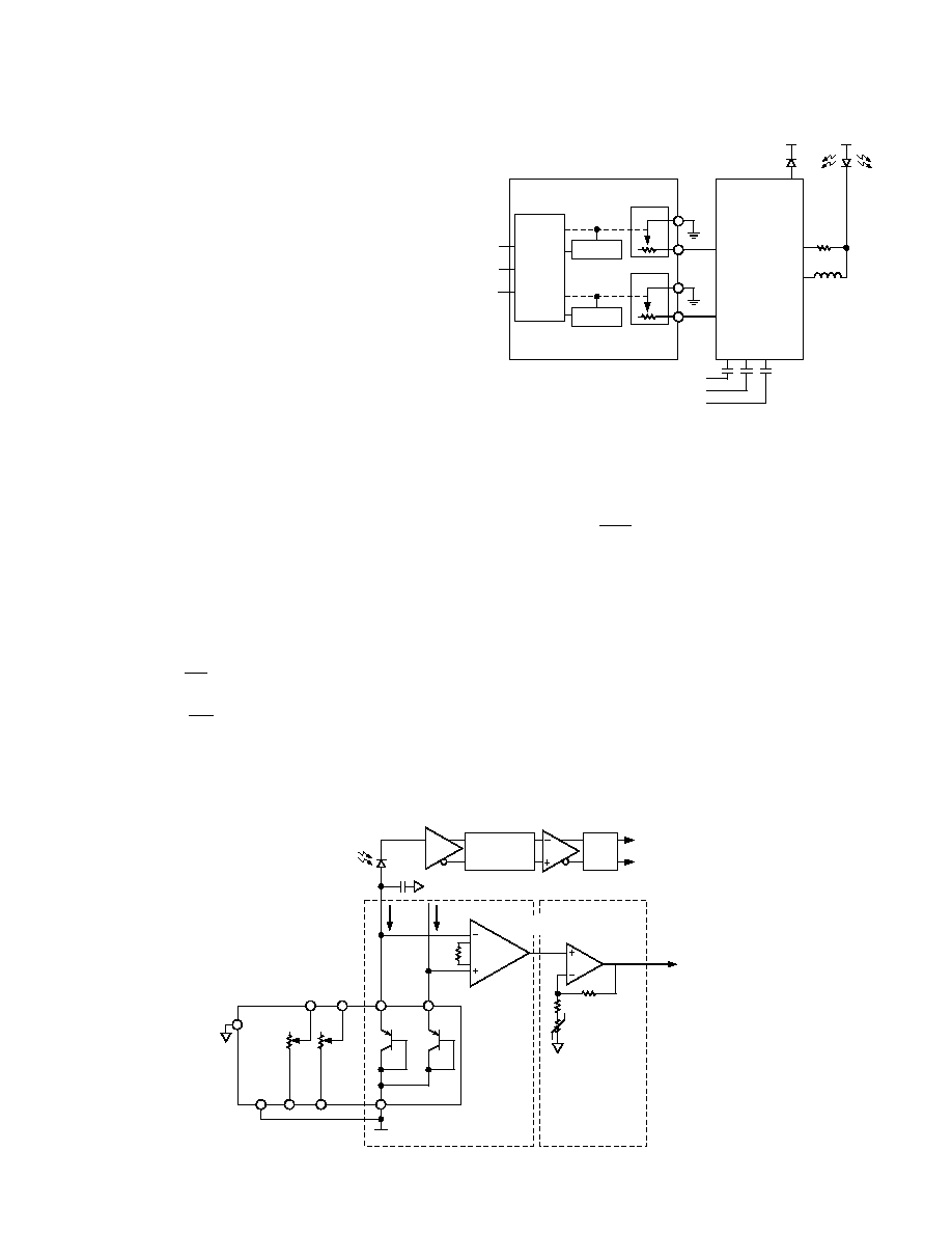
Optical Transmitter Calibration with ADN2841
Together with the multirate 2.7 Gbps Laser Diode Driver ADN2841,
the ADN2850 forms an optical supervisory system where the dual
programmable resistors are used to set the laser average optical
power and extinction ratio (see Figure 11). The ADN2850 is
particularly ideal for the optical parameter settings because of its
high resolution, compact footprint, and superior temperature
coefficient characteristics.
The ADN2841 is a 2.7 Gbps laser diode driver that uses a unique
control algorithm to manage both the laser average power and
extinction ratio after the laser initial factory calibration. It stabilizes
the laser data transmission by continuously monitoring its optical
power, and correcting the variations caused by temperature and
the laser degradation over time. In the ADN2841, the I
MPD
monitors
the laser diode current. Through its dual-loop power and extinction
ratio control, calibrated by the ADN2850, the internal driver
controls the bias current I
BIAS
and consequently the average power.
It also regulates the modulation current I
MODP
by changing the
modulation current linearly with slope efficiency. Any changes in
the laser threshold current or slope efficiency are therefore com-
pensated. As a result, this optical supervisory system minimizes the
laser characterization efforts and enables designers to apply com-
parable lasers from multiple sources.
Incoming Optical Power Monitoring
The ADN2850 comes with a pair of matched diode connected
PNPs, Q
1
and Q
2
, that can be used to configure an incoming optical
power monitoring function. With a reference current source, an
instrumentation amplifier, and a logarithmic amplifier, this feature
can be used to monitor the optical power by knowing the dc
average photodiode current from the following relationships:
V = V
= V
1
BE1
T
In
I
I
C
S
1
1
(2)
V = V
= V I
2
BE2
T
n
I
I
C
S
2
2
(3)
CS
CLK
SDI
RDAC1
W1
B1
EEMEM
ADN2841
PSET
ERSET
I
MODP
I
BIAS
IMPD
DIN
DINQ
IDT
ONE
DIN
DINQ
IDTONE
RDAC2
W2
B2
EEMEM
CONTROL
ADN2850
V
CC
V
CC
Figure 11. Optical Supervisory System
Knowing I
C1
= a
1
I
PD,
I
C2
= a
2
I
REF,
and Q
1
≠ Q
2
are matched,
therefore a and I
S
are matched. Combining Equations 2 and 3
theoretically yields:
V ≠ V = V In
T
2
1
I
I
REF
PD
(4)
Where I
S1
and I
S2
are saturation current
V
1
, V
2
are V
BE
, base-emitted voltages of the diode connector
transistors
V
T
is the thermal voltage, which is equal to k
◊ T/q.
V
T
= 26 mV at 25
∞C
k = Boltzmann's constant = 1.38E≠23 Joules/Kelvin
q = electron charge = 1.6E≠19 coulomb
T = temperature in Kelvin
I
PD
= photodiode current
I
REF
= reference current
Figure 12 shows such a conceptual circuit.

REV. B
ADN2850
≠17≠
The output voltage represents the average incoming optical power.
The output voltage of the log stage does not have to be accurate
from device to device, as the responsivity of the photodiode will
change between devices. An op amp stage is shown after the log
amp stage, which compensates for V
T
variation over temperature.
Equation 4 is ideal. If the reference current is 1 mA at room
temperature, characterization shows that there is an additional
30 mV offset between V
2
and V
1
. A curve fit approximation yields
V
V = 0.026
In
0.001
2 --
1
◊
+
I
PD
0 03
.
(5)
Such offset is believed to be caused by the transistors self-heating
and the thermal gradient effect. As seen in Figure 13, the error
between an approximation and the actual performance ranges is
less than 0% to ≠4% from 0.1 mA to 0.1 A.
0.30
0.25
0.20
0.15
0.10
0.05
0
12
9
6
3
0
≠3
≠6
1.E-07
1.E-06
1.E-05
1.E-04
1.E-03
V
2
≠
V
1
≠
V
APPR
O
X
IMA
T
ING ERR
OR ≠ %
I
PD
≠ A
I
REF
= 1mA
T
A
= 25 C
DEVICE 1
DEVICE 2
DEVICE 3
CURVE FIT
ERROR
Figure 13. Typical V
2
≠ V
1
vs. I
PD
at I
REF
= 1 mA
and T
A
= 25
∞C
Resistance Scaling
The ADN2850 offers either 25 k
or 250 k full-scale resistance.
Users who need lower resistance and still maintain the numbers
of step adjustment can parallel two or more devices. Figure 14
shows a simple scheme of paralleling both channels of the pro-
grammable resistors. In order to adjust half of the resistance
linearly per step, users need to program both devices coherently
with the same settings. Note that since the devices will be pro-
grammed one after another, an intermediate state will occur, and
this method may not be suitable for certain applications.
B1
W1
W2
B2
Figure 14. Reduce Resistance by Half with Linear
Adjustment Characteristics
Much lower resistance can also be achieved by paralleling a
discrete resistor as shown in Figure 15.
B1
W1
R
Figure 15. Resistor Scaling with Pseudo-Log Taper
Adjustment Characteristics
The equivalent resistance at a given setting is approximated as:
R =
D
R
eq
WB_FS
◊
+
◊
+
+
◊
51200
51200 1024
D
R
R
WB
FS
_
(6)
In this approach, the adjustment is not linear but pseudo-
logarithmic. Users should be aware of the need for tolerance matching
as well as temperature coefficient matching of the components.
BASIC RDAC SPICE MODEL
RDAC
25k
W
C
W
= 80pF
C
B
= 11pF
B
Figure 16. RDAC Circuit Simulation Model (RDAC = 25 k
)
The internal parasitic capacitances and the external capacitive
loads dominate the ac characteristics of the RADCs. A general
parasitic simulation model is shown in Figure 16.
Listing I provides a macro model net list for the 25 k
RDAC:
Listing I. Macro Model Net List for RDAC
.PARAM D = 1024, RDAC = 25E3
*
.SUBCKT RDAC (W, B)
*
RWB W B {D/1024 RDAC
50}
CW W 0 80E-12
CB B 0 11E-12
*
.ENDS RDAC
REV. B
≠18≠
ADN2850
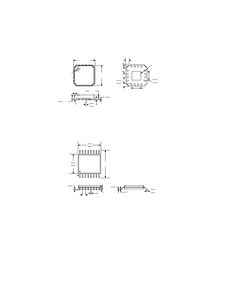
OUTLINE DIMENSIONS
16-Lead Frame Chip Scale Package [LFCSP]
5 x 5 mm Body
(CP-16 5x5)
Dimensions shown in millimeters
16
5
13
8
9
12
1
4
BOTTOM
VIEW
3.25
3.10
2.95
0.75
0.60
0.50
0.80 BSC
2.40 BSC
0.40
0.33
0.28
12
MAX
0.20 REF
SEATING
PLANE
PIN 1
INDICATOR
TOP
VIEW
5.0
BSC SQ
4.75
BSC SQ
0.60 MAX
0.60 MAX
0.05 MAX
0.01 NOM
0.70 MAX
0.65 NOM
PIN 1
INDICATOR
COPLANARITY
0.08
0.90 MAX
0.85 NOM
COMPLIANT TO JEDEC STANDARDS MO-220VHHB
16-Lead Thin Shrink Small Outline Package [TSSOP]
(RU-16)
Dimensions shown in millimeters
16
9
8
1
PIN 1
SEATING
PLANE
8
0
4.50
4.40
4.30
6.40
BSC
5.10
5.00
4.90
0.65
BSC
0.15
0.05
1.20
MAX
0.20
0.09
0.75
0.60
0.45
0.30
0.19
COPLANARITY
0.10
COMPLIANT TO JEDEC STANDARDS MO-153AB

REV. B
ADN2850
≠19≠
Revision History
Location
Page
9/02--Data sheet changed from REV. A to REV. B.
Changes to GENERAL DESCRIPTION . . . . . . . . . . . . . . . . . . . . . . . . . . . . . . . . . . . . . . . . . . . . . . . . . . . . . . . . . . . . . . . . . . . . . 1
Changes to ELECTRICAL CHARACTERISTICS . . . . . . . . . . . . . . . . . . . . . . . . . . . . . . . . . . . . . . . . . . . . . . . . . . . . . . . . . . . . . 2
Changes to Calculating Actual Full-Scale Resistance section . . . . . . . . . . . . . . . . . . . . . . . . . . . . . . . . . . . . . . . . . . . . . . . . . . . . . . 9
Changes to Table VI . . . . . . . . . . . . . . . . . . . . . . . . . . . . . . . . . . . . . . . . . . . . . . . . . . . . . . . . . . . . . . . . . . . . . . . . . . . . . . . . . . . . .9
Updated OUTLINE DIMENSIONS . . . . . . . . . . . . . . . . . . . . . . . . . . . . . . . . . . . . . . . . . . . . . . . . . . . . . . . . . . . . . . . . . . . . . . . 18

C02660≠0≠9/02(B)
PRINTED IN U.S.A.
≠20≠