 | –≠–ª–µ–∫—Ç—Ä–æ–Ω–Ω—ã–π –∫–æ–º–ø–æ–Ω–µ–Ω—Ç: ADP1110 | –°–∫–∞—á–∞—Ç—å:  PDF PDF  ZIP ZIP |
REV. 0
Information furnished by Analog Devices is believed to be accurate and
reliable. However, no responsibility is assumed by Analog Devices for its
use, nor for any infringements of patents or other rights of third parties
which may result from its use. No license is granted by implication or
otherwise under any patent or patent rights of Analog Devices.
a
ADP1110
One Technology Way, P.O. Box 9106, Norwood, MA 02062-9106, U.S.A.
Tel: 617/329-4700
World Wide Web Site: http://www.analog.com
Fax: 617/326-8703
© Analog Devices, Inc., 1996
Micropower, Step-Up/Step-Down Switching
Regulator; Adjustable and Fixed 3.3 V, 5 V, 12 V
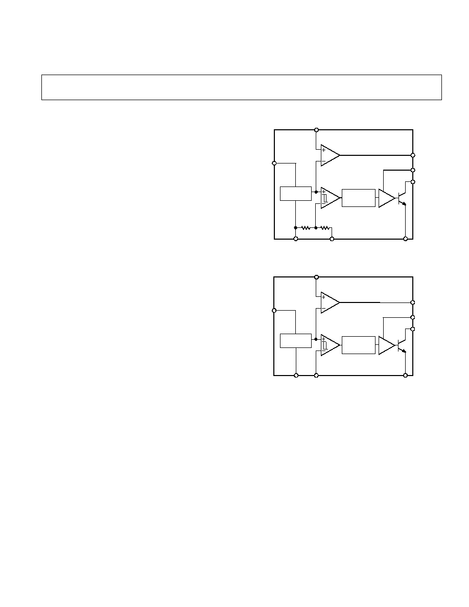
FUNCTIONAL BLOCK DIAGRAMS
SENSE
A0
DRIVER
I
LIM
SW1
SW2
V
IN
SET
220mV
REFERENCE
GAIN BLOCK/
ERROR AMP
A2
A1
Q1
OSCILLATOR
ADP1110
GND
COMPARATOR
R1
R2
300k
ADP1110 Block Diagram--Fixed Output Version
A0
DRIVER
I
LIM
SW1
SW2
V
IN
GND
SET
220mV
REFERENCE
GAIN BLOCK/
ERROR AMP
COMPARATOR
FB
A2
A1
Q1
OSCILLATOR
ADP1110
ADP1110 Block Diagram--Adjustable Output Version
FEATURES
Operates at Supply Voltages From 1.0 V to 30 V
Step-Up or Step-Down Mode
Minimal External Components Required
Low-Battery Detector
User-Adjustable Current Limiting
Fixed or Adjustable Output Voltage Versions
8-Pin DIP or SO-8 Package
APPLICATIONS
Cellular Telephones
Single-Cell to 5 V Converters
Laptop and Palmtop Computers
Pagers
Cameras
Battery Backup Supplies
Portable Instruments
Laser Diode Drivers
Hand-Held Inventory Computers
GENERAL DESCRIPTION
The ADP1110 is part of a family of step-up/step-down switch-
ing regulators that operate from an input voltage supply as little
as 1.0 V. This very low input voltage allows the ADP1110 to be
used in applications that use a single cell as the primary power
source.
The ADP1110 can be configured to operate in either step-up or
step-down mode, but for input voltages greater than 3 V, the
ADP1111 would be a more effective solution.
An auxiliary gain amplifier can serve as a low battery detector or
as a linear regulator.
The quiescent current of 300
µ
A makes the ADP1110 useful in
remote or battery powered applications.
The 70 kHz frequency operation also allows for the use of
surface-mount external capacitors and inductors.
Battery protection circuitry limits the effect of reverse current to
safe levels at reverse voltages up to 1.6 V.

≠2≠
REV. 0
ADP1110≠SPECIFICATIONS
Parameter
Conditions
V
S
Min
Typ
Max
Units
QUIESCENT CURRENT
Switch Off
I
Q
300
µ
A
INPUT VOLTAGE
Step-Up Mode
V
IN
1.15
12.6
V
Step-Down Mode
30
V
COMPARATOR TRIP POINT VOLTAGE
ADP1110
1
210
220
230
mV
OUTPUT SENSE VOLTAGE
ADP1110-3.3
2
V
OUT
3.13
3.30
3.47
V
ADP1110-5
2
4.75
5.00
5.25
V
ADP1110-12
2
11.4
12.00
12.6
V
COMPARATOR HYSTERESIS
ADP1110
4
8
mV
OUTPUT HYSTERESIS
ADP1110-3.3
66
130
mV
ADP1110-5
90
180
mV
ADP1110-12
200
400
mV
OSCILLATOR FREQUENCY
f
OSC
52
70
90
kHz
DUTY CYCLE
Full Load (V
FB
< V
REF
)
DC
62
69
78
%
SWITCH ON TIME
t
ON
7.5
10
12.5
µ
s
FEEDBACK PIN BIAS CURRENT
ADP1110 V
FB
= 0 V
I
FB
150
240
nA
SET PIN BIAS CURRENT
V
SET
= V
REF
I
SET
300
500
nA
A0 OUTPUT LOW
I
AO
= 300
µ
A
V
AO
0.15
0.4
V
V
SET
= 150 mV
REFERENCE LINE REGULATION
1.0 V
V
IN
1.5 V
0.35
%/V
1.5 V
V
IN
12 V
0.05
0.1
%/V
SWITCH SATURATION VOLTAGE
V
IN
= 1.5 V, I
SW
= 400 mA, +25
∞
C
V
CESAT
300
500
mV
STEP-UP MODE
T
MIN
to T
MAX
600
mV
V
IN
= 1.5 V, I
SW
= 500 mA, +25
∞
C
400
650
mV
T
MIN
to T
MAX
750
mV
V
IN
= 5 V, I
SW
= 1 A, +25
∞
C
700
1000
mV
A2 ERROR AMP GAIN
R
L
= 100 k
3
A
V
1000
5000
V/V
REVERSE BATTERY CURRENT
T
A
= +25
∞
C
4
I
REV
750
mA
CURRENT LIMIT TEMPERATURE
V
IN,
T
A
= +25
∞
C
≠0.3
%/
∞
C
COEFFICIENT
SWITCH OFF LEAKAGE CURRENT
Measured at SW1 Pin,
I
LEAK
1
10
µ
A
T
A
= +25
∞
C
MAXIMUM EXCURSION BELOW GND
I
SW1
10
µ
A, Switch Off
V
SW2
≠400
≠350
mV
T
A
= +25
∞
C
NOTES
1
This specification guarantees that both the high and low trip point of the comparator fall within the 210 mV to 230 mV range.
2
This specification guarantees that the output voltage of the fixed versions will always fall within the specified range. The waveform at the sense pin will exhibit a saw-
tooth shape due to the comparator hysteresis.
3
100 k
resistor connected between a 5 V source and the AO pin.
4
The ADP1110 is guaranteed to withstand continuous application of +1.6 V applied to the GND and SW2 pins while V
IN
, I
LIM
, and SW1 pins are grounded.
5
All limits at temperature extremes are guaranteed via correlation using standard statistical quality control methods.
Specifications subject to change without notice.
(0 C to +70 C, V
IN
= 1.5 V unless otherwise noted)

ADP1110
≠3≠
REV. 0
PIN DESCRIPTION
Mnemonic
Function
I
LIM
For normal conditions this pin is connected to
V
IN
. When lower current is required, a resistor
should be connected between I
LIM
and V
IN
.
Limiting the switch current to 400 mA is
achieved by connecting a 220
resistor.
V
IN
Input Voltage.
SW1
Collector Node of Power Transistor. For step-
down configuration, connect to V
IN
. For step-
up configuration, connect to an inductor/diode.
SW2
Emitter Node of Power Transistor. For step-
down configuration, connect to inductor/diode.
For step-up configuration, connect to ground.
Do not allow this pin to go more than a diode
drop below ground.
GND
Ground.
AO
Auxiliary Gain (GB) Output. The open collec-
tor can sink 300
µ
A. It can be left open if unused.
SET
Gain Amplifier Input. The amplifier has posi-
tive input connected to SET pin and negative
input connected to 220 mV reference. It can be
left open if unused.
FB/SENSE
On the ADP1110 (adjustable) version this pin
is connected to the comparator input. On the
ADP1110-3.3, ADP1110-5 and ADP1110-12,
the pin goes directly to the internal application
resistor that set output voltage.
ABSOLUTE MAXIMUM RATINGS
Input Supply Voltage, Step-Up Mode . . . . . . . . . . . . . . . 15 V
Input Supply Voltage, Step-Down Mode . . . . . . . . . . . . . 36 V
SW1 Pin Voltage . . . . . . . . . . . . . . . . . . . . . . . . . . . . . . . 50 V
SW2 Pin Voltage . . . . . . . . . . . . . . . . . . . . . . . . . ≠0.5 V to V
IN
Feedback Pin Voltage (ADP1110) . . . . . . . . . . . . . . . . . . 5.5 V
Switch Current . . . . . . . . . . . . . . . . . . . . . . . . . . . . . . . . 1.5 A
Maximum Power Dissipation . . . . . . . . . . . . . . . . . . 500 mW
Operating Temperature Range . . . . . . . . . . . . . 0
∞
C to +70
∞
C
Storage Temperature Range . . . . . . . . . . . . . ≠65
∞
C to 150
∞
C
Lead Temperature (Soldering, 10 sec) . . . . . . . . . . . . . 300
∞
C
TYPICAL APPLICATION
1.5V
AA CELL*
I
LIM
V
IN
SW1
SW2
GND
ADP1110-5
47µH
5V
15µF
TANTALUM
SENSE
OPERATES WITH CELL VOLTAGE
1.0V
*ADD 10µF DECOUPLING CAPACITOR IF BATTERY IS
*
MORE THAN 2' AWAY FROM ADP1110.
1
2
3
4
5
8
Figure 1. 1.5 V to 5 V Converter
ORDERING GUIDE
Model
Output Voltage
Package
ADP1110AN
ADJ
N-8
ADP1110AR
ADJ
SO-8
ADP1110AN-3.3
3.3 V
N-8
ADP1110AR-3.3
3.3 V
SO-8
ADP1110AN-5
5 V
N-8
ADP1110AR-5
5 V
SO-8
ADP1110AN-12
12 V
N-8
ADP1110AR-12
12 V
SO-8
WARNING!
ESD SENSITIVE DEVICE
CAUTION
ESD (electrostatic discharge) sensitive device. Electrostatic charges as high as 4000 V readily
accumulate on the human body and test equipment and can discharge without detection.
Although the ADP1110 features proprietary ESD protection circuitry, permanent damage may
occur on devices subjected to high energy electrostatic discharges. Therefore, proper ESD
precautions are recommended to avoid performance degradation or loss of functionality.
8-Lead SOIC
(SO-8)
A0
I
LIM
SW1
GND
V
IN
SW2
FB (SENSE)*
SET
1
2
3
4
8
7
6
5
TOP VIEW
(Not to Scale)
ADP1110
*FIXED VERSIONS
T
JMAX
= 90
o
,
JA
= 150
o
C/W
8-Lead Plastic DIP
(N-8)
A0
I
LIM
SW1
GND
V
IN
SW2
*FIXED VERSIONS
FB (SENSE)*
SET
1
2
3
4
8
7
6
5
ADP1110
TOP VIEW
(Not to Scale)
T
JMAX
= 90
o
,
JA
= 130
o
C/W
PIN CONFIGURATIONS
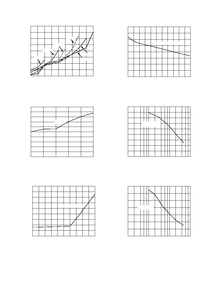
ADP1110-Typical Characteristics
≠4≠
REV. 0
I
SWITCH
CURRENT ≠ A
1.4
0
0.1
1.4
0.2
0.4
0.5
0.6
0.8
1
1.2
1.25
1.2
0.6
0.4
0.2
1
0.8
V
IN
= +1V
V
IN
= +1.2V
V
IN
= +1.5V
V
IN
= +2V
V
IN
= +3V
V
IN
= +5V
SATURATION VOLTAGE ≠ V
Figure 2. Saturation Voltage vs. I
SWITCH
Current in Step-Up
Mode
I
SWITCH
CURRENT ≠ A
2
1.8
0
0.1
0.9
0.2
0.4
0.6
0.8
1.2
0.6
0.4
0.2
1.6
1.4
0.8
1
V
IN
= +12V
ON VOLTAGE ≠ V
Figure 3. Switch ON Voltage vs. I
SWITCH
Current In Step-
Down Mode
INPUT VOLTAGE ≠ V
1
30
3
6
9
12
15
18
21
24
27
1800
0
1600
1400
1200
1000
800
600
400
200
QUIESCENT CURRENT
QUIESCENT CURRENT ≠ µA
Figure 4. Quiescent Current vs. Input Voltage
76
66
60
2
30
4
6
8
10
12
15
18
21
24
27
74
68
64
62
72
70
INPUT VOLTAGE ≠ V
OSCILLATOR FREQUENCY ≠ kHz
OSCILLATOR FREQUENCY
Figure 5. Oscillator Frequency vs. Input Voltage
R
LIM
≠
1.9
1.7
0.1
1
1000
10
100
1.5
1.3
0.5
1.1
0.9
0.7
0.3
SWITCH CURRENT ≠ A
STEP-DOWN WITH
V = +12V
Figure 6. Maximum Switch Current vs. R
LIM
R
LIM
≠
0.1
1
1000
10
100
1.5
1.3
0.5
1.1
0.9
0.7
0.3
STEP-UP MODE
WITH V
+5V
SWITCH CURRENT ≠ A
Figure 7. Maximum Switch Current vs. R
LIM
ADP1110
≠5≠
REV. 0
TEMPERATURE ≠ C
78
76
64
0
70
25
72
70
68
66
74
OSCILLATOR FREQUENCY
OSCILLATOR FREQUENCY ≠ kHz
Figure 8. Oscillator Frequency vs. Temperature
TEMPERATURE ≠ C
ON TIME ≠ µs
9.0
8.9
8.2
0
70
25
8.6
8.5
8.4
8.3
8.8
8.7
SWITCH ON TIME
Figure 9. Switch ON Time vs. Temperature
TEMPERATURE ≠ C
66
65
59
0
70
25
63
62
61
60
64
DUTY CYCLE
DUTY CYCLE ≠ %
Figure 10. Duty Cycle vs. Temperature
TEMPERATURE ≠ C
0.54
0.53
0.47
0
70
25
0.51
0.5
0.49
0.48
0.52
V
IN
= +1.5
@
I
SWITCH
= +0.5A
V
CE(SAT)
≠ V
Figure 11. Switch ON Voltage Step-Down vs. Temperature
TEMPERATURE ≠ C
350
300
0
0
70
25
200
150
100
50
250
QUIESCENT CURRENT
QUIESCENT CURRENT ≠ µA
Figure 12. Quiescent Current vs. Temperature
TEMPERATURE ≠ C
160
120
0
70
25
145
140
135
125
155
150
BIAS CURRENT
BIAS CURRENT ≠ nA
130
Figure 13. FB Pin Bias Current vs. Temperature

ADP1110
≠6≠
REV. 0
THEORY OF OPERATION
The ADP1110 is a flexible, low-power, switch-mode power
supply (SMPS) controller. The regulated output voltage can be
greater than the input voltage (boost or step-up mode) or less
than the input (buck or step-down mode). This device uses a
gated-oscillator technique to provide very high performance with
low quiescent current.
A functional block diagram of the ADP1110 is shown on the
first page. The internal 220 mV reference is connected to one
input of the comparator, while the other input is externally
connected (via the FB pin) to a feedback network connected to
the regulated output. When the voltage at the FB pin falls below
220 mV, the 70 kHz oscillator turns on. A driver amplifier provides
base drive to the internal power switch, and the switching action
raises the output voltage. When the voltage at the FB pin exceeds
220 mV, the oscillator is shut off. While the oscillator is off, the
ADP1110 quiescent current is only 300
µ
A. The comparator
includes a small amount of hysteresis, which ensures loop
stability without requiring external components for frequency
compensation.
The maximum current in the internal power switch can be set
by connecting a resistor between V
IN
and the I
LIM
pin. When the
maximum current is exceeded, the switch is turned OFF. The
current limit circuitry has a time delay of about 800 ns. If an
external resistor is not used, connect I
LIM
to V
IN
. Further informa-
tion on I
LIM
is included in the "Applications" section of this data
sheet.
The ADP1110 internal oscillator provides 10
µ
s ON and 5
µ
s
OFF times, which is ideal for applications where the ratio between
V
IN
and V
OUT
is roughly a factor of three (such as generating +5 V
from a single 1.5 V cell). Wider range conversions, as well as
step-down converters, can also be accomplished with a slight
loss in the maximum output power that can be obtained.
An uncommitted gain block on the ADP1110 can be connected
as a low≠battery detector. The inverting input of the gain block
is internally connected to the 220 mV reference. The noninverting
input is available at the SET pin. A resistor divider, connected
between V
IN
and GND with the junction connected to the SET
pin, causes the AO output to go LOW when the low battery set
point is exceeded. The AO output is an open collector NPN
transistor that can sink 300
µ
A.
The ADP1110 provides external connections for both the
collector and emitter of its internal power switch, which permits
both step-up and step-down modes of operation. For the step-
up mode, the emitter (Pin SW2) is connected to GND and the
collector (Pin SW1) drives the inductor. For step-down mode,
the emitter drives the inductor while the collector is connected
to V
IN
.
The output voltage of the ADP1110 is set with two external
resistors. Three fixed-voltage models are also available:
ADP1110≠3.3 (+3.3 V), ADP1110≠5 (+5 V) and ADP1110-12
(+12 V). The fixed-voltage models are identical to the
ADP1110 except that laser-trimmed voltage-setting resistors are
included on the chip. Only three external components are
required to form a +3.3 V, +5 V or +12 V converter. On the
fixed-voltage models of the ADP1110, simply connect the
SENSE pin (Pin 8) directly to the output voltage.
COMPONENT SELECTION
General Notes on Inductor Selection
When the ADP1110 internal power switch turns on, current
begins to flow in the inductor. Energy is stored in the inductor
core while the switch is on, and this stored energy is then
transferred to the load when the switch turns off. Because both
the collector and the emitter of the switch transistor are
accessible on the ADP1110, the output voltage can be higher,
lower, or of opposite polarity than the input voltage.
To specify an inductor for the ADP1110, the proper values of
inductance, saturation current, and DC resistance must be
determined. This process is not difficult, and specific equations
for each circuit configuration are provided in this data sheet. In
general terms, however, the inductance value must be low
enough to store the required amount of energy (when both
input voltage and switch ON time are at a minimum) but high
enough that the inductor will not saturate when both V
IN
and
switch ON time are at their maximum values. The inductor
must also store enough energy to supply the load without
saturating. Finally, the dc resistance of the inductor should be
low so that excessive power will not be wasted by heating the
windings. For most ADP1110 applications, an inductor of
15
µ
H to 100
µ
H with a saturation current rating of 300 mA to
1A and dc resistance <0.4
is suitable. Ferrite-core inductors
that meet these specifications are available in small, surface-
mount packages.
To minimize Electro-Magnetic Interference (EMI), a toroid or
pot-core type inductor is recommended. Rod-core inductors are
a lower-cost alternative if EMI is not a problem.
TEMPERATURE ≠ C
400
0
0
70
25
250
200
150
50
350
300
BIAS CURRENT
BIAS CURRENT ≠ nA
100
Figure 14. Set Pin Bias Current vs. Temperature
V
REF
≠ mV
TEMPERATURE ≠ C
220
219
211
0
70
25
215
214
213
212
217
216
218
REFERENCE VOLTAGE
Figure 15. Reference Voltage vs. Temperature

ADP1110
≠7≠
REV. 0
CALCULATING THE INDUCTOR VALUE
Selecting the proper inductor value is a simple three-step
process:
1. Define the operating parameters: minimum input voltage,
maximum input voltage, output voltage and output current.
2. Select the appropriate conversion topology (step-up, step-
down, or inverting).
3. Calculate the inductor value, using the equations in the
following sections.
INDUCTOR SELECTION≠STEP-UP CONVERTER
In a step-up or boost converter (Figure 19), the inductor must
store enough power to make up the difference between the input
voltage and the output voltage. The power that must be stored
is calculated from the equation:
P
L
=
V
OUT
+
V
D
-
V
IN MIN
(
)
(
)
∑
I
OUT
(
)
(Equation 1)
where V
D
is the diode forward voltage (
0.5 V for a 1N5818
Schottky). Because energy is only stored in the inductor while
the ADP1110 switch is ON, the energy stored in the inductor
on each switching cycle must be must be equal to or greater
than:
P
f
L
OSC
(Equation 2)
in order for the ADP1110 to regulate the output voltage.
When the internal power switch turns ON, current flow in the
inductor increases at the rate of:
I
L
(t)
=
V
IN
R'
1
-
e
≠R't
L
(Equation 3)
where L is in Henrys and R' is the sum of the switch equivalent
resistance (typically 0.8
at +25
∞
C) and the dc resistance of
the inductor. If the voltage drop across the switch is small
compared to V
IN
, a simpler equation can be used:
I
L
(t)
=
V
IN
L
t
(Equation 4)
Replacing `t' in the above equation with the ON time of the
ADP1110 (10
µ
s, typical) will define the peak current for a
given inductor value and input voltage. At this point, the
inductor energy can be calculated as follows:
E
L
=
1
2
L
∑
I
2
PEAK
(Equation 5)
As previously mentioned, E
L
must be greater than P
L
/f
OSC
so
that the ADP1110 can deliver the necessary power to the load.
For best efficiency, peak current should be limited to 1 A or
less. Higher switch currents will reduce efficiency because of
increased saturation voltage in the switch. High peak current also
increases output ripple. As a general rule, keep peak current as low
as possible to minimize losses in the switch, inductor and diode.
In practice, the inductor value is easily selected using the equations
above. For example, consider a supply that will generate 12 V at
120 mA from a 4.5 V to 8 V source. The inductor power required
is from Equation 1:
P
L
=
12 V
+
0.5 V
-
4.5 V
(
)
∑
120 mA
=
960 mW
On each switching cycle, the inductor must supply:
P
L
f
OSC
=
960 mW
70 kHz
=
13.7
µ
J
Assuming a peak current of 1 A as a starting point, (Equation 4)
can be rearranged to recommend an inductor value:
L
=
V
IN
I
L(MAX )
t
=
4.5V
1 A
10
µ
s
=
45
µ
H
Substituting a standard inductor value of 47
µ
H with 0.2
dc
resistance will produce a peak switch current of:
I
PEAK
=
4.5V
1.0
1
-
e
≠1.0
∑
10
µ
s
47
µ
H
=
862 mA
Once the peak current is known, the inductor energy can be
calculated from Equation 5:
E
L
=
1
2
47
µ
H
(
)
∑
862 mA
(
)
2
=
17.5
µ
J
Since the inductor energy of 17.5
µ
J is greater than the P
L
/f
OSC
requirement of 13.7
µ
J, the 47
µ
H inductor will work in this
application. By substituting other inductor values into the same
equations, the optimum inductor value can be determined.
When selecting an inductor, the peak current must not exceed
the maximum switch current of 1.5 A.
The peak current must be evaluated for both minimum and
maximum values of input voltage. If the switch current is high
when V
IN
is at its minimum, the 1.5 A limit may be exceeded at the
maximum value of V
IN
. In this case, the ADP1110's current limit
feature can be used to limit switch current. Simply select a resistor
(using Figure 7) that will limit the maximum switch current to the
I
PEAK
value calculated for the minimum value of V
IN
. This will
improve efficiency by producing a constant I
PEAK
as V
IN
increases.
See the "Limiting the Switch Current" section of this data sheet for
more information.
Note that the switch current limit feature does not protect the
circuit if the output is shorted to ground. In this case, current is
only limited by the dc resistance of the inductor and the forward
voltage of the diode.
INDUCTOR SELECTION≠STEP-DOWN CONVERTER
The step-down mode of operation is shown in Figure 20.
Unlike the step-up mode, the ADP1110's power switch does not
saturate when operating in the step-down mode; therefore,
switch current should be limited to 800 mA in this mode. If the
input voltage will vary over a wide range, the I
LIM
pin can be
used to limit the maximum switch current. Higher switch
current is possible by adding an external switching transistor as
shown in Figure 22.
The first step in selecting the step-down inductor is to calculate
the peak switch current as follows:
I
PEAK
=
2 I
OUT
DC
V
OUT
+
V
D
V
IN
≠V
SW
+
V
D
(Equation 6)
where: DC = duty cycle (0.69 for the ADP1110)
V
SW
= voltage drop across the switch
V
D
= diode drop (0.5 V for a 1N5818)
I
OUT
= output current
V
OUT
= the output voltage
V
IN
= the minimum input voltage

ADP1110
≠8≠
REV. 0
As previously mentioned, the switch voltage is higher in step-
down mode than in step-up mode. V
SW
is a function of switch
current and is therefore a function of V
IN
, L, time and V
OUT
.
For most applications, a V
SW
value of 1.5 V is recommended.
The inductor value can now be calculated:
L
=
V
IN(MIN )
≠V
SW
≠V
OUT
I
PEAK
∑
t
ON
(Equation 7)
where: t
ON
= Switch ON time (10
µ
s)
If the input voltage will vary (such as an application that must
operate from a 9 V, 12 V or 15 V source), an R
LIM
resistor
should be selected from Figure 6. The R
LIM
resistor will keep
switch current constant as the input voltage rises. Note that
there are separate R
LIM
values for step-up and step-down modes
of operation.
For example, assume that +5 V at 250 mA is required from a
+9 V to +18 V source. Deriving the peak current from Equation
6 yields:
I
PEAK
=
2
∑
250 mA
0.69
5
+
0.5
9
-
1.5
+
0.5
=
498 mA
Then, the peak current can be inserted into Equation 7 to
calculate the inductor value:
L
=
9 ≠1.5 ≠ 5
498 mA
∑
10
µ
s
=
50
µ
s
Since 50
µ
H is not a standard value, the next lower standard
value of 47
µ
H would be specified.
To avoid exceeding the maximum switch current when the
input voltage is at +18 V, an R
LIM
resistor should be specified.
Using the step-down curve of Figure 6, a value of 560
will
limit the switch current to 500 mA.
INDUCTOR SELECTION--POSITIVE-TO-NEGATIVE
CONVERTER
The configuration for a positive-to-negative converter using the
ADP1110 is shown in Figure 23. As with the step-up converter,
all of the output power for the inverting circuit must be supplied
by the inductor. The required inductor power is derived from
the formula:
P =
I
L
OUT
V
V
OUT
D
+
(
)
∑
(
)
(Equation 8)
The ADP1110 power switch does not saturate in positive-to-
negative mode. The voltage drop across the switch can be
modeled as a 0.75 V base-emitter diode in series with a 0.65
resistor. When the switch turns on, inductor current will rise at
a rate determined by:
I
L
(t)
=
V
L
R'
1
-
e
≠R't
L
(Equation 9)
where: R' = 0.65
+ R
L(DC)
V
L
= V
IN
≠ 0.75 V
For example, assume that a ≠5 V output at 75 mA is to be
generated from a +4.5 V to +5.5 V source. The power in the
inductor is calculated from Equation 8:
P
L
=
|≠ 5V|
+
0.5V
(
)
∑
75 mA
(
)
=
413 mW
During each switching cycle, the inductor must supply the
following energy:
P
L
f
OSC
=
413 mW
70 kHz
=
5.9
µ
J
Using a standard inductor value of 56
µ
H with 0.2
dc
resistance will produce a peak switch current of:
I
PEAK
=
4.5V ≠ 0.75V
0.65
+
0.2
1
-
e
≠0.85
∑
10
µ
s
56
µ
H
=
621 mA
Once the peak current is known, the inductor energy can be
calculated from Equation 9:
E
L
=
1
2
56
µ
H
(
)
∑
621 mA
(
)
2
=
10.8
µ
J
Since the inductor energy of 10.8
µ
J is greater than the P
L
/f
OSC
requirement of 5.9
µ
J, the 56
µ
H inductor will work in this
application.
The input voltage only varies between 4.5 V and 5.5 V in this
example. Therefore, the peak current will not change enough to
require an R
LIM
resistor and the I
LIM
pin can be connected
directly to V
IN
. Care should be taken, of course, to ensure that
the peak current does not exceed 800 mA.
CAPACITOR SELECTION
For optimum performance, the ADP1110's output capacitor
must be selected carefully. Choosing an inappropriate capacitor
can result in low efficiency and/or high output ripple.
Ordinary aluminum electrolytic capacitors are inexpensive but
often have poor Equivalent Series Resistance (ESR) and
Equivalent Series Inductance (ESL). Low ESR aluminum
capacitors, specifically designed for switch mode converter
applications, are also available, and these are a better choice
than general purpose devices. Even better performance can be
achieved with tantalum capacitors, although their cost is higher.
Very low values of ESR can be achieved by using OS-CON
capacitors (Sanyo Corporation, San Diego, CA). These devices
are fairly small, available with tape-and-reel packaging and have
very low ESR.
The effects of capacitor selection on output ripple are demon-
strated in Figures 16, 17 and 18. These figures show the output
of the same ADP1110 converter, that was evaluated with three
different output capacitors. In each case, the peak switch
current is 500 mA, and the capacitor value is 100
µ
F. Figure 16
shows a Panasonic HF-series 16-volt radial cap. When the
switch turns off, the output voltage jumps by about 90 mV and
then decays as the inductor discharges into the capacitor. The
rise in voltage indicates an ESR of about 0.18
. In Figure 17,
the aluminum electrolytic has been replaced by a Sprague 293D
series, a 6 V tantalum device. In this case the output jumps

ADP1110
≠9≠
REV. 0
about 30 mV, which indicates an ESR of 0.06
. Figure 18
shows an OS-CON 16≠volt capacitor in the same circuit, and
ESR is only 0.02
.
10
0%
100
90
1µs
50mV
Figure 16. Aluminum Electrolytic
10
0%
100
90
1µs
50mV
Figure 17. Tantalum Electrolytic
10
0%
100
90
1µs
50mV
Figure 18. OS-CON Capacitor
If low output ripple is important, the user should consider the
ADP3000. Because this device switches at 400 kHz, lower peak
current can be used. Also, the higher switching frequency
simplifies the design of the output filter. Consult the ADP3000
data sheet for additional details.
DIODE SELECTION
In specifying a diode, consideration must be given to speed,
forward voltage drop and reverse leakage current. When the
ADP1110 switch turns off, the diode must turn on rapidly if
high efficiency is to be maintained. Shottky rectifiers, as well as
fast signal diodes such as the 1N4148, are appropriate. The
forward voltage of the diode represents power that is not
delivered to the load, so V
F
must also be minimized. Again,
Schottky diodes are recommended. Leakage current is especially
important in low-current applications, where the leakage can be
a significant percentage of the total quiescent current.
For most circuits, the 1N5818 is a suitable companion to the
ADP1110. This diode has a V
F
of 0.5 V at 1 A, 4
µ
A to 10
µ
A
leakage, and fast turn-on and turn-off times. A surface mount
version, the MBRS130LT3, is also available.
For switch currents of 100 mA or less, a Shottky diode such as
the BAT85 provides a V
F
of 0.8 V at 100 mA and leakage less
than 1
µ
A. A similar device, the BAT54, is available in a SOT23
package. Even lower leakage, in the 1 nA to 5 nA range, can be
obtained with a 1N4148 signal diode.
General purpose rectifiers, such as the 1N4001, are not suitable
for ADP1110 circuits. These devices, which have turn-on times
of 10
µ
s or more, are too slow for switching power supply
applications. Using such a diode "just to get started" will result
in wasted time and effort. Even if an ADP1110 circuit appears
to function with a 1N4001, the resulting performance will not
be indicative of the circuit performance when the correct diode
is used.
CIRCUIT OPERATION, STEP-UP (BOOST) MODE
In boost mode, the ADP1110 produces an output voltage that is
higher than the input voltage. For example, +5 V can be derived
from one alkaline cell (+1.5 V), or +12 V can be generated from
a +5 V logic power supply.
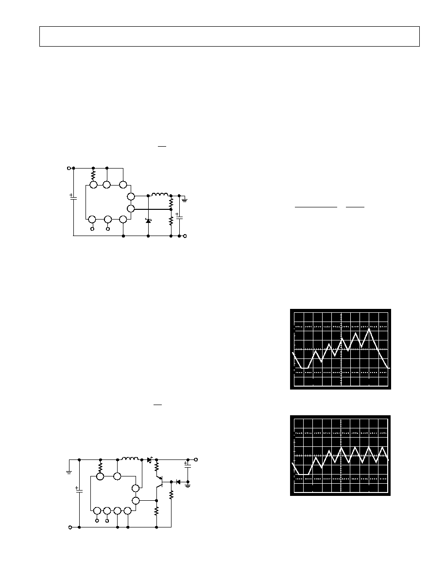
Figure 19 shows an ADP1110 configured for step-up operation.
The collector of the internal power switch is connected to the
output side of the inductor, while the emitter is connected to
GND. When the switch turns on, pin SW1 is pulled near
ground. This action forces a voltage across L1 equal to V
IN
≠
V
CE(SAT),
and current begins to flow through L1. This current
reaches a final value (ignoring second-order effects) of:
I
PEAK
V
IN
≠V
CE(SAT )
L
∑
10
µ
s
where 10
µ
s is the ADP1110 switch's "on" time.
I
LIM
V
IN
SW1
SW2
FB
GND
ADP1110
L1
C
1
R1
R2
D1
8
1
2
3
4
5
V
IN
V
OUT
R3*
*OPTIONAL
Figure 19. Step-Up Mode Operation
When the switch turns off, the magnetic field collapses. The
polarity across the inductor changes, current begins to flow
through D1 into the load, and the output voltage is driven above
the input voltage.
The output voltage is fed back to the ADP1110 via resistors R1
and R2. When the voltage at pin FB falls below 220 mV, SW1

ADP1110
≠10≠
REV. 0
turns "on" again, and the cycle repeats. The output voltage is
therefore set by the formula:
V
OUT
=
220 mV
∑
1
+
R1
R2
The circuit of Figure 19 shows a direct current path from V
IN
to
V
OUT
, via the inductor and D1. Therefore, the boost converter
is not protected if the output is short circuited to ground.
CIRCUIT OPERATION, STEP-DOWN (BUCK) MODE
The ADP1110's step-down mode is used to produce an output
voltage that is lower than the input voltage. For example, the
output of four NiCd cells (+4.8 V) can be converted to a +3 V
logic supply.
A typical configuration for step-down operation of the ADP1110 is
shown in Figure 20. In this case, the collector of the internal
power switch is connected to V
IN
and the emitter drives the
inductor. When the switch turns on, SW2 is pulled up towards
V
IN
. This forces a voltage across L1 equal to V
IN
≠ V
CE
≠ V
OUT
and causes current to flow in L1. This current reaches a final
value of:
I
PEAK
V
IN
-
V
CE
-
V
OUT
L
∑
10
µ
s
where 10
µ
s is the ADP1110 switch's "on" time.
I
LIM
V
IN
SW1
SW2
GND
SET
AO
ADP1110
NC
NC
L1
C
1
R1
R2
D1
1N5818
V
OUT
C
2
V
IN
2
R
LIM
100
FB
1
3
6
7
5
4
8
Figure 20. Step-Down Mode Operation
When the switch turns off, the magnetic field collapses. The
polarity across the inductor changes, and the switch side of the
inductor is driven below ground. Schottky diode D1 then turns
on, and current flows into the load. Notice that the Absolute
Maximum Rating for the ADP1110's SW2 pin is 0.5 V below
ground. To avoid exceeding this limit, D1 must be a Schottky
diode. Using a silicon diode in this application will generate
forward voltages above 0.5 V that will cause potentially
damaging power dissipation within the ADP1110.
The output voltage of the buck regulator is fed back to the
ADP1110's FB pin by resistors R1 and R2. When the voltage at
pin FB falls below 220 mV, the internal power switch turns
"on" again and the cycle repeats. The output voltage is set by
the formula:
V
OUT
=
220 mV
∑
1
+
R1
R2
When operating the ADP1110 in step-down mode, the output
voltage is impressed across the internal power switch's emitter-
base junction when the switch is off. To protect the switch, the
output voltage should be limited to 6.2 V or less. If a higher
output voltage is required, a Schottky diode should be placed in
series with SW2, as shown in Figure 21.
I
LIM
V
IN
SW1
SW2
FB
GND
SET
AO
ADP1110
NC
NC
L1
C
L
R1
R2
D1
1N5818
OUTPUT
C
INPUT
INPUT
6
7
8
1
2
3
4
5
R
LIM
Figure 21. Step-Down Mode, V
OUT
> 6.2 V
If the input voltage to the ADP1110 varies over a wide range, a
current limiting resistor at Pin 1 may be required. If a particular
circuit requires high peak inductor current with minimum input
supply voltage, the peak current may exceed the switch maxi-
mum rating and/or saturate the inductor when the supply
voltage is at the maximum value. See the "Limiting the Switch
Current" section of this data sheet for specific recommendations.
INCREASING OUTPUT CURRENT IN THE STEP-DOWN
REGULATOR
Unlike the boost configuration, the ADP1110's internal power
switch is not saturated when operating in step-down mode. A
conservative value for the voltage across the switch in step-down
mode is 1.5 V. This results in high power dissipation within the
ADP1110 when high peak current is required. To increase the
output current, an external PNP switch can be added (Figure
22). In this circuit, the ADP1110 provides base drive to Q1
through R3, while R4 ensures that Q1 turns off rapidly. Because
the ADP1110's internal current limiting function will not work
in this circuit, R5 is provided for this purpose. With the value
shown, R5 limits current to 2 A. In addition to reducing power
dissipation on the ADP1110, this circuit also reduces the switch
voltage. When selecting an inductor value for the circuit of
Figure 22, the switch voltage can be calculated from the
formula:
V
SW
=
V
R5
+
V
Q1(SAT )
0.6V
+
0.4V
1V
I
LIM
V
IN
SW1
SW2
FB
GND
SET
AO
ADP1110
NC
NC
L1
C
L
R1
R2
D1
1N5821
OUTPUT
C
INPUT
R
LIM
INPUT
6
7
8
1
2
4
5
3
R4
220
R3
330
MJE210
0.3
R5
Figure 22. High Current Step-Down Operation
ADP1110
≠11≠
REV. 0
POSITIVE-TO-NEGATIVE CONVERSION
The ADP1110 can convert a positive input voltage to a negative
output voltage as shown in Figure 23. This circuit is essentially
identical to the step-down application of Figure 19, except that
the "output" side of the inductor is connected to power ground.
When the ADP1110's internal power switch turns off, current
flowing in the inductor forces the output (≠V
OUT
) to a negative
potential. The ADP1110 will continue to turn the switch on
until its FB pin is 220 mV above its GND pin, so the output
voltage is determined by the formula:
V
OUT
=
220 mV
∑
1
+
R1
R2
ILIM
VIN
SW1
SW2
FB
GND
SET
AO
ADP1110
NC
NC
L1
C
L
R1
R2
D1
1N5818
OUTPUT
C
INPUT
R
LIM
INPUT
6
7
8
1
2
4
5
3
NEGATIVE
OUTPUT
Figure 23. A Positive-to-Negative Converter
The design criteria for the step-down application also apply to
the positive-to-negative converter. The output voltage should be
limited to |6.2 V| unless a diode is inserted in series with the
SW2 pin (see Figure 21.) Also, D1 must again be a Schottky
diode to prevent excessive power dissipation in the ADP1110.
NEGATIVE-TO-POSITIVE CONVERSION
The circuit of Figure 24 converts a negative input voltage to a
positive output voltage. Operation of this circuit configuration is
similar to the step-up topology of Figure 19, except the current
through feedback resistor R1 is level-shifted below ground by a
PNP transistor. The voltage across R1 is V
OUT
≠ V
BEQ1
. However,
diode D2 level-shifts the base of Q1 about 0.6 V below ground
thereby cancelling the V
BE
of Q1. The addition of D2 also reduces
the circuit's output voltage sensitivity to temperature, which other-
wise would be dominated by the ≠2 mV V
BE
contribution of Q1.
The output voltage for this circuit is determined by the formula:
V
OUT
=
220 mV
∑
R1
R2
Unlike the positive step-up converter, the negative-to-positive
converter's output voltage can be either higher or lower than the
input voltage.
I
LIM
V
IN
SW1
SW2
FB
GND
SET
AO
ADP1110
NC
NC
L1
C
L
R2
D1
C
INPUT
R
LIM
6
7
8
1
2
4
5
3
POSITIVE
OUTPUT
10K
NEGATIVE
INPUT
Q1
2N3906
D2
1N4148
R1
Figure 24. A Negative-to-Positive Converter
LIMITING THE SWITCH CURRENT
The ADP1110's R
LIM
pin permits the switch current to be
limited with a single resistor. This current limiting action occurs
on a pulse by pulse basis. This feature allows the input voltage
to vary over a wide range without saturating the inductor or
exceeding the maximum switch rating. For example, a particular
design may require peak switch current of 800 mA with a 2.0 V
input. If V
IN
rises to 4 V, however, the switch current will
exceed 1.6 A. The ADP1110 limits switch current to 1.5 A and
thereby protects the switch, but the output ripple will increase.
Selecting the proper resistor will limit the switch current to
800 mA, even if V
IN
increases. The relationship between R
LIM
and maximum switch current is shown in Figure 6.
The I
LIM
feature is also valuable for controlling inductor current
when the ADP1110 goes into continuous-conduction mode.
This occurs in the step-up mode when the following condition is
met:
V
OUT
+
V
D IODE
V
IN
≠ V
SW
<
1
1≠ DC
where DC is the ADP1110's duty cycle. When this relationship
exists, the inductor current does not go all the way to zero
during the time that the switch is OFF. When the switch turns
on for the next cycle, the inductor current begins to ramp up
from the residual level. If the switch ON time remains constant,
the inductor current will increase to a high level (see Figure 25).
This increases output ripple and can require a larger inductor
and capacitor. By controlling switch current with the I
LIM
resistor, output ripple current can be maintained at the design
values. Figure 26 illustrates the action of the I
LIM
circuit.
10
0%
100
90
10µs
10mV
200mA/div.
Figure 25. I
LIM
Operation--I
L
Characteristic
10
0%
100
90
10µs
10mV
200mA/div.
Figure 26. I
LIM
Operation--I
L
Characteristic
ADP1110
≠12≠
REV. 0
The internal structure of the I
LIM
circuit is shown in Figure 27.
Q1 is the ADP1110's internal power switch, that is paralleled by
sense transistor Q2. The relative sizes of Q1 and Q2 are scaled
so that I
Q2
is 0.5% of I
Q1
. Current flows to Q2 through an
internal 80
resistor and through the R
LIM
resistor. These two
resistors parallel the base-emitter junction of the oscillator-
disable transistor, Q3. When the voltage across R1 and R
LIM
exceeds 0.6 V, Q3 turns on and terminates the output pulse. If
only the 80
internal resistor is used (i.e., the I
LIM
pin is
connected directly to V
IN
), the maximum switch current will be
1.5 A. Figure 6 gives R
LIM
values for lower current-limit values.
72kHz
OSC
V
IN
POWER
SWITCH
SW2
SW1
R
LIM
DRIVER
80
(INTERNAL)
I
LIM
IQ1
V
IN
200
(EXTERNAL)
Q2
ADP1110
R1
Q3
Q1
Figure 27. ADP1110 Current Limit Operation
The delay through the current limiting circuit is approximately
800 ns. If the switch ON time is reduced to less than 3
µ
s,
accuracy of the current trip-point is reduced. Attempting to
program a switch ON time of 800 ns or less will produce
spurious responses in the switch ON time; however, the
ADP1110 will still provide a properly-regulated output voltage.
PROGRAMMING THE GAIN BLOCK
The gain block of the ADP1110 can be used as a low-battery
detector, error amplifier or linear post regulator. The gain block
consists of an op amp with PNP inputs and an open-collector
NPN output. The inverting input is internally connected to the
ADP1110's 220 mV reference, while the noninverting input is
available at the SET pin. The NPN output transistor will sink
about 300
µ
A.
Figure 28 shows the gain block configured as a low-battery
monitor. Resistors R1 and R2 should be set to high values to
reduce quiescent current, but not so high that bias current in
the SET input causes large errors. A value of 33 k
for R2 is a
good compromise. The value for R1 is then calculated from the
formula:
R1
=
V
LOBATT
≠ 220 mV
220 mV
R2
where V
LOBATT
is the desired low battery trip point. Since the
gain block output is an open-collector NPN, a pull-up resistor
should be connected to the positive logic power supply.
ADP1110
GND
AO
R
L
R1
V
BAT
SET
R2
33k
220V
V
REF
R
HYS
V
LOGIC
Figure 28. Setting the Low Battery Detector Trip Point
The circuit of Figure 28 may produce multiple pulses when
approaching the trip point due to noise coupled into the SET
input. To prevent multiple interrupts to the digital logic,
hysteresis can be added to the circuit. Resistor R
HYS
, with a
value of 1 M
to 10 M
, provides the hysteresis. The addition
of R
HYS
will change the trip point slightly, so the new value for
R1 will be:
R1
=
V
LOBATT
≠ 220 mV
220 mV
R2
≠
V
L
≠ 220 mV
R
L
+
R
HYS
where V
L
is the logic power supply voltage, R
L
is the pull-up
resistor, and R
HYS
creates the hysteresis.
The gain block can also be used as a control element to reduce
output ripple. The ADP3000 is normally recommended for low-
ripple applications, but its minimum input voltage is 2 V. The
gain-block technique using the ADP1110 can be useful for step-
up converters operating down to 1 V.
A step-up converter using this technique is shown in Figure 29.
This configuration uses the gain block to sense the output
voltage and control the comparator. The result is that the
comparator hysteresis is reduced by the open loop gain of the
gain block. Output ripple can be reduced to only a few millivolts
with this technique, versus a typical value of 90 mV for a +5 V
converter using just the comparator. For best results, a large
output capacitor (1000
µ
F or more) should be specified. This
technique can also be used for step-down or inverting applica-
tions, but the ADP3000 is usually a more appropriate choice.
See the ADP3000 data sheet for further details.
I
LIM
V
IN
SW1
SW2
FB GND
SET
AO
ADP1110
L1
C
L
R1
R2
OUTPUT
C
INPUT
INPUT
6
7
8
1
2
4
5
3
1000µF
300k
13.8k
270k
10µF
D1
CTX15-4
1N5818
15µH
Figure 29. Using the Gain Block to Reduce Output Ripple

ADP1110
≠13≠
REV. 0
APPLICATION CIRCUITS
All-Surface-Mount, Single-Cell to 5 V Converter
This is a very simple, compact, low-part-count circuit that takes
a single alkaline 1.5 V cell input and produces a 5 V output.
The output current should be kept to 10 mA or less to conserve
battery life.
I
LIM
V
IN
SW1
SW2
SENSE
GND
SET
AO
ADP1110-5
NC
NC
L1
D1
1N5817
6
7
8
1
2
4
5
3
50µH
+5V
10mA
15µF
C
L
ONE
ALKALINE
CELL
CTX50-4
1.5V
Figure 30. All-Surface-Mount, Single-Cell to 5 V Converter
All-Surface-Mount, 3 V to 5 V Step-Up Converter
Similar to the previous circuit, this circuit takes a 3-volt input
and provides a 5 V output at 40 mA. As in the single-cell version,
the circuit is compact and uses only four external components.
I
LIM
V
IN
SW1
SW2
SENSE
GND
SET
AO
ADP1110-5
NC
NC
L1
6
7
8
1
2
4
5
3
220
3V
50µH
+5V
40mA
10µF
C
L
TWO
ALKALINE
CELLS
D1
1N5817
CTX50-4
Figure 31. All-Surface-Mount, 3 V to 5 V Step-Up
Converter
All-Surface-Mount, 9 V to 5 V Step-Down Converter
Featuring the same low parts count of the step-up design, this
circuit is the complement to the preceding one. The 220
resistor programs the current limit to around 600 mA.
I
LIM
V
IN
SW1
SW2
SENSE
GND
SET
AO
ADP1110-5
NC
NC
L1
D1
6
8
1
2
4
5
3
220
50µH
1N5817
+5V
40mA
10µF
C
L
9V
BATTERY
7
R
LIM
CTX50-4
Figure 32. All-Surface-Mount, 9 V to 5 V Step-Down
Converter
1.5 V to 5 V Dual-Output Step-Up Converter
This circuit works from a single 1.5 V cell and provides simulta-
neous outputs of +5 V and ≠5 V. The accuracy of the negative
output suffers slightly because of the extra diode drop of around
0.4 V.
I
LIM
V
IN
SW1
SW2
SENSE
GND
SET
AO
ADP1110-5
NC
NC
6
7
8
1
2
4
5
3
1.5V
L16
8µH
4.7µF
ONE
ALKALINE
CELL
4.7µF
+5V
3mA
NOTE: ALL DIODES 1N5818
≠5V
3mA
4.7µF
CTX68-4
Figure 33. 1.5 V to
±
5 V Dual-Output Step-Up
Converter
All-Surface-Mount Flash Memory VPP Generator
Figure 34 shows a circuit that can generate the programming
voltage, VPP to program flash memory. The key components
are the MOSFET and the bipolar transistor. These two devices
form a switch that, when ON, allows the ADP1110 to power-up
and function as a step-up converter. The output is +12 V at 120
mA. When the MOSFET switch is OFF, the output of the
circuit drops to just under +5 V thereby disabling the program-
ming capability.
Care should be taken so there is no short-circuit-current limiting
in the circuit in either operating mode.
I
LIM
V
IN
SW1
SW2
SENSE
GND
SET
AO
ADP1110-12
NC
NC
6
7
8
1
2
4
5
3
L1
50µH
10µF
C
L
LOGIC1 = PROGRAM
LOGIC0 = SHUTDOWN
D1
1N5818
CTX50-4
MMBT4403
1k
MMBF170
V
PP
+12V
120mA
+5V
10k
Figure 34. All Surface-Mount Flash Memory VPP Generator

ADP1110
≠14≠
REV. 0
1.5 V to +5 V, +10 V Dual Output Step-Up Converter
The circuit of Figure 35 illustrates a way to get outputs of
+10 V and +5 V from the same converter. The main 5 V output
is derived from the feedback provided by the 487 k
and 11 k
resistors. Capacitor C1 should be a multilayer ceramic variety
for best performance, but a good quality tantalum capacitor will
also give good performance at lower cost.
I
LIM
V
IN
SW1
SW2
FB
GND
SET
AO
ADP1110
NC
NC
6
7
8
1
2
4
5
3
1.5V
L1
50µH
4.7µF
ONE
ALKALINE
CELL
4.7µF
NOTE: ALL DIODES 1N5818
CTX50-4
+5V
3mA
11k
487k
+10V
3mA
D1
D2
D3
220
Figure 35. 1.5 V to +5 V, +10 V Dual Output Step-Up
Converter
1.5 V-Powered Laser Diode Driver
Figure 36 shows a circuit suitable for driving many laser diodes
that incorporate a photodiode to monitor the laser diode
current, this circuit makes use of the gain block and current-
limit functions to provide a feedback system based on the
average laser diode current. This current must be controlled
very closely or permanent damage to the laser diode is likely to
be the result.
To ensure that the laser is operating at the proper power level,
the actual optical power from the laser should be monitored
with a calibrated photodiode or optical power meter. In
addition, the actual diode current should also be monitored, and
R1 can be adjusted to give the correct output power.
NOTES
1. All inductors referenced are Coiltronics CTX-series except
where noted.
2. If the source of power is more than an inch or so from the
converter, the input to the converter should be bypassed with
approximately 10
µ
F of capacitance. This capacitor should be
a good quality tantalum or aluminum electrolytic.
I
LIM
V
IN
SW1
SW2
FB
GND
SET
AO
ADP1110
6
7
8
1
2
4
5
3
10
1N4148
220
1.5V
5.1k
0.022µF
1k
2.2µH
1µF
2
1N5818
MJE210
TOSHIBA
TOLD-9321
100µF
OS-Con
2N3906
1k
Figure 36. 1.5 V-Powered Laser Diode Driver
ADP1110
≠15≠
REV. 0
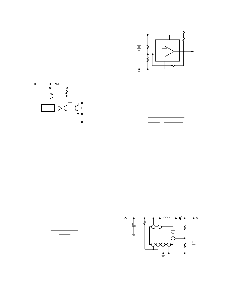
8-Lead Plastic DIP
(N-8)
8
1
4
5
0.430 (10.92)
0.348 (8.84)
0.280 (7.11)
0.240 (6.10)
PIN 1
SEATING
PLANE
0.022 (0.558)
0.014 (0.356)
0.060 (1.52)
0.015 (0.38)
0.210 (5.33)
MAX
0.130
(3.30)
MIN
0.070 (1.77)
0.045 (1.15)
0.100
(2.54)
BSC
0.160 (4.06)
0.115 (2.93)
0.325 (8.25)
0.300 (7.62)
0.015 (0.381)
0.008 (0.204)
0.195 (4.95)
0.115 (2.93)
8-Lead SOIC
(SO-8)
0.1968 (5.00)
0.1890 (4.80)
8
5
4
1
0.2440 (6.20)
0.2284 (5.80)
PIN 1
0.1574 (4.00)
0.1497 (3.80)
0.0688 (1.75)
0.0532 (1.35)
SEATING
PLANE
0.0098 (0.25)
0.0040 (0.10)
0.0192 (0.49)
0.0138 (0.35)
0.0500
(1.27)
BSC
0.0098 (0.25)
0.0075 (0.19)
0.0500 (1.27)
0.0160 (0.41)
8
∞
0
∞
0.0196 (0.50)
0.0099 (0.25)
x 45
∞
OUTLINE DIMENSIONS
Dimensions shown in inches and (mm).

≠16≠
C2212≠12≠10/96
PRINTED IN U.S.A.