 | –≠–ª–µ–∫—Ç—Ä–æ–Ω–Ω—ã–π –∫–æ–º–ø–æ–Ω–µ–Ω—Ç: ADP1821 | –°–∫–∞—á–∞—Ç—å:  PDF PDF  ZIP ZIP |
Document Outline
- FEATURES
- APPLICATIONS
- GENERAL DESCRIPTION
- ˛ˇ
- ˛ˇ
- ˛ˇ
- ˛ˇ
- ˛ˇ
- ˛ˇ
- ˛ˇ
- ˛ˇ
- ˛ˇ
- ˛ˇ
- ˛ˇ
- ˛ˇ
- ˛ˇ
- ˛ˇ
- ˛ˇ
- ˛ˇ
- ˛ˇ
- ˛ˇ
- ˛ˇ
20 A Step-Down DC-DC Controller
ADP1821
Rev. 0
Information furnished by Analog Devices is believed to be accurate and reliable.
However, no responsibility is assumed by Analog Devices for its use, nor for any
infringements of patents or other rights of third parties that may result from its use.
Specifications subject to change without notice. No license is granted by implication
or otherwise under any patent or patent rights of Analog Devices. Trademarks and
registered trademarks are the property of their respective owners.
One Technology Way, P.O. Box 9106, Norwood, MA 02062-9106, U.S.A.
Tel: 781.329.4700
www.analog.com
Fax: 781.461.3113
© 2005 Analog Devices, Inc. All rights reserved.
FEATURES
Wide input voltage range: 1 V to 24 V
Wide output voltage range: 0.6 V to 85% of input voltage
1% accuracy, 0.6 V reference voltage
All N-channel MOSFET
300 kHz, 600 kHz, or up to 1.2 MHz synchronized frequency
No current sense resistor required
Power-good output
Programmable soft start with reverse current protection
Current limit protection
Thermal overload protection
Overvoltage protection
Undervoltage lockout
1
A shutdown supply current
Small, 16-lead QSOP package
APPLICATIONS
Telecom and networking systems
High performance servers
Medical imaging systems
DSP core power supplies
Microprocessor core power supplies
Mobile communication base stations
Distributed power
GENERAL DESCRIPTION
The ADP1821 is a versatile and inexpensive, synchronous PWM
step-down controller. It drives an all N-channel power stage to
regulate an output voltage as low as 0.6 V with up to a 20 A load
current.
The ADP1821 is well suited for a wide range of high power appli-
cations, such as DSP and processor core power in telecom, medical
imaging, high performance servers, and industrial applications. It
operates from a 3.0 V to 5.5 V supply with a power input voltage
ranging from 1.0 V to 24 V.
The ADP1821 can operate at any frequency between 300 KHz and
1.2 MHz either by synchronizing with an external source or an
internally generated, logic controlled clock of 300 KHz or
600 KHz. It includes an adjustable soft start to allow sequencing
and quick power-up while preventing input inrush current. Output
reverse-current protection at startup prevents excessive output
voltage excursions. The adjustable virtually lossless current limit
scheme reduces external part count and improves efficiency.
The ADP1821 operates over the ≠40∞C to +85∞C temperature range
and is available in a 16-lead QSOP package.
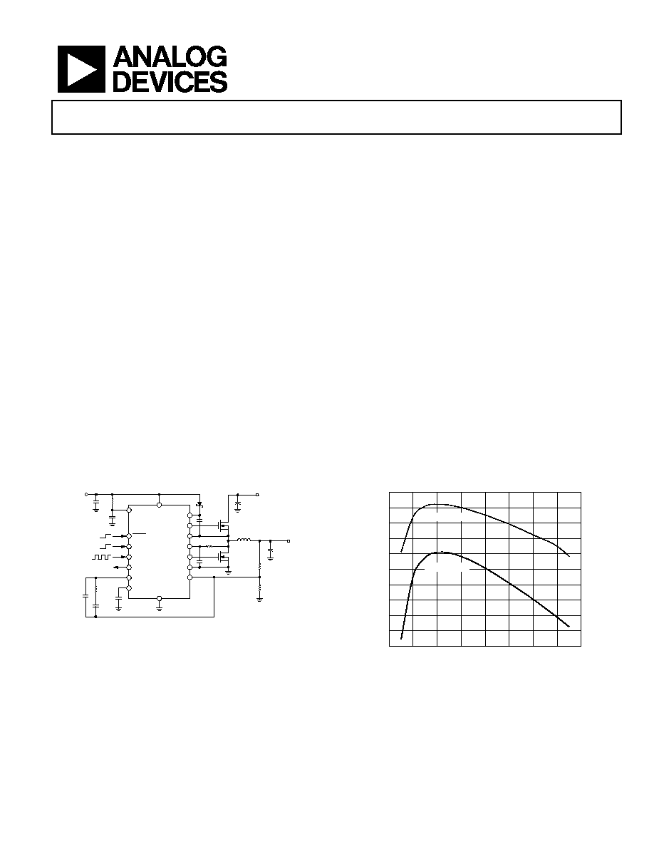
VCC
FREQ
SYNC
PWGD
COMP
SS
BST
DH
SW
CSL
DL
PGND
FB
PVCC
GND
BIAS INPUT
5V
1
F
10
100nF
ADP1821
IRF3711
IRF3711
1
H
180
F
20V
POWER INPUT
2.25V TO 20V
1000
F
4V
OUTPUT
1.8V, 15A
0.1
F
2.2pF
6.18k
05310-
001
80.6k
15pF
1
F
CMOSH-3
390pF
20k
10k
SHDN
Figure 1. Typical Operating Circuit
97
87
0
1
LOAD CURRENT (A)
E
FFICIE
NCY
(%)
6
96
95
94
93
92
91
90
89
88
2
4
6
8
10
12
14
1.8V OUTPUT
3.3V OUTPUT
05310-006
Figure 2. Efficiency vs. Load Current, 5 V Input

ADP1821
Rev. 0 | Page 2 of 20
TABLE OF CONTENTS
Specifications..................................................................................... 3
Absolute Maximum Ratings............................................................ 5
ESD Caution.................................................................................. 5
Simplified Block Diagram ............................................................... 6
Pin Configuration and Function Descriptions............................. 7
Typical Performance Characteristics ............................................. 8
Theory of Operation ...................................................................... 10
Current Limit Scheme ............................................................... 10
Soft Start ...................................................................................... 10
High-Side Driver (BST and DH).............................................. 10
Low-Side Driver (DL) ................................................................ 10
Input Voltage Range ................................................................... 11
Setting the Output Voltage ........................................................ 11
Switching Frequency Control ................................................... 11
Compensation............................................................................. 11
Power-Good Indicator............................................................... 11
Shutdown Control...................................................................... 11
Application Information................................................................ 12
Selecting the Input Capacitor ................................................... 12
Output LC Filter ......................................................................... 12
Selecting the MOSFETS ............................................................ 13
Setting the Current Limit .......................................................... 13
Feedback Voltage Divider ......................................................... 13
Compensating the Regulator .................................................... 14
Setting the Soft Start Period...................................................... 16
Synchronizing the Converter.................................................... 16
Application Circuits ....................................................................... 17
Outline Dimensions ....................................................................... 18
Ordering Guide .......................................................................... 18
REVISION HISTORY
7/05--Revision 0: Initial Version
ADP1821
Rev. 0 | Page 3 of 20
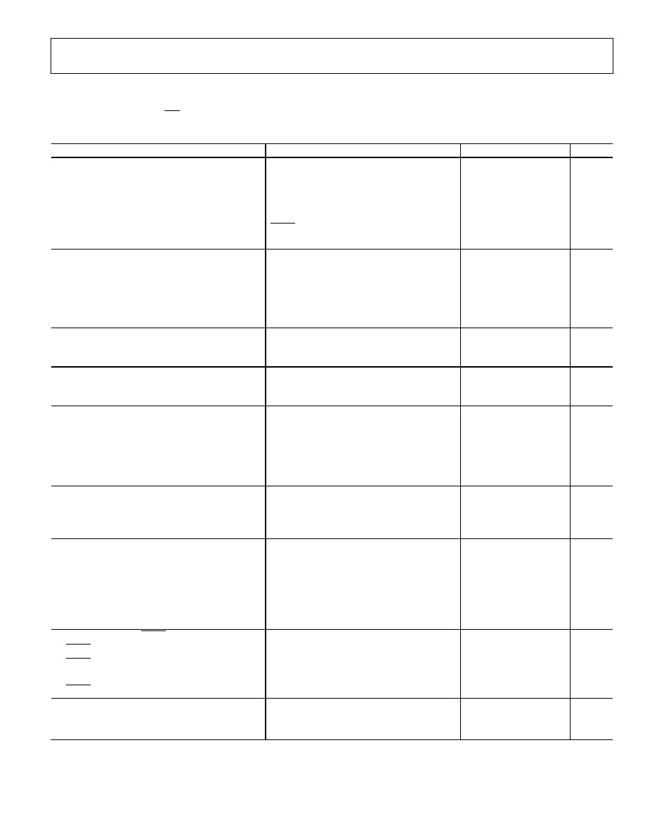
SPECIFICATIONS
See Figure 1. V
VCC
= V
PVCC
=V
SHDN
= V
FREQ
= 5 V, SYNC = GND. All limits at temperature extremes are guaranteed via correlation using standard
statistical quality control (SQC). T
A
= 25∞C, unless otherwise specified.
Table 1.
Parameter Conditions
Min
Typ
Max
Unit
POWER SUPPLY
Input Voltage
3.0
5.5
V
Undervoltage Lockout Threshold
V
VCC
rising
2.5
2.7
2.9
V
Undervoltage Lockout Hysteresis
V
VCC
0.1
V
Quiescent Current
I
VCC
+ I
VCC
, not switching
1
2
mA
Shutdown Current
SHDN = GND
10
A
Power Stage Supply Voltage
1.0
20
V
ERROR AMPLIFER
FB Regulation Voltage
T
A
= -40
∞C to +85∞C
594 600 606 mV
FB Input Bias Current
≠100
+1
+100
nA
Error Amplifier Open-Loop Voltage Gain
70
dB
COMP Output Sink Current
600
A
COMP Output Source Current
110
A
PWM CONTROLLER
PWM Peak Ramp Voltage
1.25
V
DL Minimum On-Time
FREQ = VCC (300 kHz)
140
170
200
ns
SOFT START
SS Pull-Up Resistance
SS = GND
95
k
SS Pull-Down Resistance
V
SS
= 0.6 V
1.65
2.5
4.2
k
OSCILLATOR
Oscillator Frequency
FREQ = GND, T
A
= -40
∞C to +85∞C
250 310 375 kHz
FREQ = VCC, T
A
= -40
∞C to +85∞C
470 570 720 kHz
Synchronization Range
FREQ = GND
300
600
kHz
FREQ = VCC
600
1200
kHz
SYNC Minimum Pulse Width
80
ns
CURRENT SENSE
CSL Threshold Voltage
Relative to PGND
-30
0
+30
mV
CSL Output Current
V
CSL
= 0 V, T
A
= -40
∞C to +85∞C
42 50 54
A
Current Sense Blanking Period
160
ns
GATE DRIVERS
DH Rise Time
C
GATE
= 3 nF, V
DH
= V
IN
, V
BST
- V
SW
= 5 V
16
ns
DH Fall Time
C
GATE
= 3 nF, V
DH
= V
IN
, V
BST
- V
SW
= 5 V
12
ns
DL Rise Time
C
GATE
= 3 nF, V
DL
= V
IN
19
ns
DL Fall Time
C
GATE
= 3 nF, V
DL
= 0 V
13
ns
DL Low to DH High Dead Time
33
ns
DH Low to DL High Dead Time
42
ns
LOGIC THRESHOLDS (SHDN, SYNC, FREQ)
SHDN, SYNC, FREQ Input High Voltage
V
VCC
= 3.0 V to 5.5 V
2.0
V
SHDN, SYNC, FREQ Input Low Voltage
V
VCC
= 3.0 V to 5.5 V
0.8
V
SYNC, FREQ Input Leakage Current
SYNC = FREQ = GND
0.1
1
A
SHDN Pull-Down Resistance
100
k
THERMAL SHUTDOWN
Thermal Shutdown Threshold
145
∞C
Thermal Shutdown Hysteresis
10
∞C

ADP1821
Rev. 0 | Page 4 of 20
Parameter Conditions
Min
Typ
Max
Unit
PWGD OUTPUT
FB Overvoltage Threshold
V
FB
rising
750
mV
FB Overvoltage Hysteresis
35
mV
FB Undervoltage Threshold
V
FB
rising
550
mV
FB Undervoltage Hysteresis
35
mV
PWGD Off Current
V
PWGD
= 5 V
1
A
PWGD Low Voltage
I
PWGD
= 10 mA
150
500
mV
ADP1821
Rev. 0 | Page 5 of 20
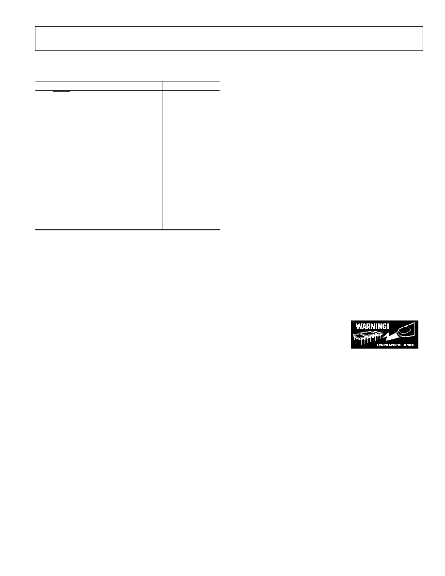
ABSOLUTE MAXIMUM RATINGS
Table 2.
Parameter Rating
VCC, SHDN, SYNC, FREQ, COMP, SS, FB to
GND, PVCC to PGND, BST to SW
-0.3 V to +6 V
BST-to-GND
-0.3 V to +30 V
CSL-to-GND
-1 V to +30 V
DH-to-GND
(V
SW
- 0.3 V) to
(V
BST
+ 0.3 V)
DL-to-PGND
-0.3 V to
(V
PVCC
+ 0.3 V)
SW-to-GND
-2 V to +30 V
PGND-to-GND
±2 V
JA
, 2-Layer (SEMI Standard Board)
150∞C/W
JA
, 4-Layer (JEDEC Standard Board)
105∞C/W
Operating Ambient Temperature
-40∞C to +85∞C
Operating Junction Temperature
-55∞C to +125∞C
Storage Temperature
-65∞C to +150∞C
Maximum Soldering Lead Temperature
260∞C
Stresses above those listed under Absolute Maximum Ratings
may cause permanent damage to the device. This is a stress
rating only; functional operation of the device at these or any
other condition s above those indicated in the operational
section of this specification is not implied. Exposure to absolute
maximum rating conditions for extended periods may affect
device reliability.
Absolute maximum ratings apply individually only, not in
combination. Unless otherwise specified all other voltages are
referenced to GND.
ESD CAUTION
ESD (electrostatic discharge) sensitive device. Electrostatic charges as high as 4000 V readily accumulate on
the human body and test equipment and can discharge without detection. Although this product features
proprietary ESD protection circuitry, permanent damage may occur on devices subjected to high energy
electrostatic discharges. Therefore, proper ESD precautions are recommended to avoid performance
degradation or loss of functionality.
ADP1821
Rev. 0 | Page 6 of 20
SIMPLIFIED BLOCK DIAGRAM
THERMAL
SHUTDOWN
LOGIC
UVLO
OSCILLATOR
FAULT
S
R
Q
Q
PWM
VCC
FAULT
REFERENCE
THSD
UVLO
OV
0.6V
UV
0.8V
100k
2.5k
BST
DH
SW
PVCC
DL
PGND
CSL
PWGD
FB
SS
COMP
SYNC
FREQ
GND
VCC
SHDN
ADP1821
05310-002
Figure 3.

ADP1821
Rev. 0 | Page 7 of 20
PIN CONFIGURATION AND FUNCTION DESCRIPTIONS
1
2
3
4
5
6
7
8
16
15
14
13
12
11
10
9
DH
SW
SYNC
PWGD
SHDN
FREQ
BST
DL
PGND
CSL
FB
GND
SS
COMP
VCC
PVCC
TOP VIEW
(Not to Scale)
ADP1821
05310-005
Figure 4. Pin Configuration
Table 3. Pin Function Description
Pin
No. Mnemonic
Description
1 BST High-Side Gate Driver Boost Capacitor Input. A capacitor between SW and BST powers the high-side gate driver
DH. The capacitor is charged through a diode from PVCC when the low-side MOSFET is on. Connect a 0.1 F or
greater ceramic capacitor from BST to SW and a Schottky diode from PVCC to BST to power the high-side gate
driver.
2 DH
High-Side Gate Driver Output. Connect DH to the gate of the external high-side, N-channel MOSFET switch. DH is
powered from the capacitor between SW and BST and its voltage swings between V
SW
and V
BST
.
3 SW
Power Switch Node. SW is the power switching node. Connect the source of the high-side, N-channel MOSFET
switch and the drain of the low-side, N-channel MOSFET synchronous rectifier to SW. SW powers the output
through the output LC filter.
4 SYNC Frequency Synchronization Input. Drive SYNC with an external 300 kHz to 1.2 MHz signal to synchronize the
converter switching frequency to the applied signal. The maximum SYNC frequency is limited to 2◊ the nominal
internal frequency selected by FREQ. Do not leave SYNC unconnected; when not used, connect SYNC to GND.
5 FREQ Frequency Select Input. FREQ selects the converter switching frequency. Drive FREQ low to select 300 kHz, or high
to select 600 kHz. Do not leave FREQ unconnected.
6
SHDN
Active-Low DC-to-DC Shutdown Input. Drive SHDN high to turn-on the converter and drive it low to turn it off.
Connect SHDN to VCC for automatic startup.
7 PWGD Open-Drain Power-Good Output. PWGD sinks current to GND when the output voltage is above or below the
regulation voltage. Connect a pull-up resistor from PWGD to VDD for a logical power-good indicator.
8
GND
Analog Ground. Connect GND to PGND at a single point as close as possible to the IC.
9 SS
Soft-Start Control Input. A capacitor from SS to GND controls the soft-start period. When the output is overloaded,
SS is discharged to prevent excessive input current while the output recovers. Connect a 1 nF to 1 F capacitor
from SS to GND to set the soft-start period. See the Soft Start section.
10 FB
Voltage Feedback Input. Connect to a resistive voltage divider from the output to FB to set the output voltage. See
the Setting the Output Voltage section.
11 COMP Compensation Node. Connect a resistor-capacitor network from COMP to FB to compensate the regulation
control system. See the Compensation section.
12 VCC
Internal Power Supply Input. VCC powers the internal circuitry. Bypass VCC to GND with 0.1 F or greater capacitor
connected as close as possible to the IC.
13 CSL
Low-Side Current Sense Input. Connect CSL to SW through a resistor to set the current limit. See the Setting the
Current Limit section.
14
PGND
Power Ground. Connect GND to PGND at a single point as close as possible to the IC.
15 DL
Low-Side Gate Driver Output. Connect DL to the gate of the low-side, N-channel MOSFET synchronous rectifier.
The DL voltage swings between PGND and PVCC.
16 PVCC Internal Gate-Driver Power Supply Input. PVCC powers the low-side, gate driver DL. Bypass PVCC to PGND with 1
F or greater capacitor connected as close as possible to the IC.

ADP1821
Rev. 0 | Page 8 of 20
LOAD CURRENT (A)
E
FFICIE
NCY
(%)
TYPICAL PERFORMANCE CHARACTERISTICS
97
87
0
16
0.6003
0.5996
≠50
110
TEMPERATURE (
∞
C)
FE
E
DBACK V
O
LTAGE
(V
)
96
95
94
93
92
91
90
89
88
0.6002
0.6001
0.6000
0.5999
0.5998
0.5997
1.8V OUTPUT
2
4
6
8
10
12
14
3.3V OUTPUT
05310-006
LOAD CURRENT (A)
E
FFICIE
NCY
(%)
≠30
≠10
10
30
50
70
90
Figure 5. Efficiency vs. Load Current, V
IN
= 5 V, V
OUT
= 3.3 V, 1.8 V
94
80
0
16
05310-009
700
0
≠50
100
TEMPERATURE (
∞
C)
S
W
ITCHING FRE
Q
UE
NCY
(k
Hz)
92
90
88
86
84
82
2
4
6
8
10
12
14
1.8V OUTPUT
3.3V OUTPUT
05310-007
Figure 6. Efficiency vs. Load Current, V
IN
= 12 V, V
OUT
= 3.3 V, 1.8 V
1400
0
0
6
VCC VOLTAGE (V)
V
CC CURRE
NT (
A)
1200
1000
800
600
400
200
1
2
3
4
5
05310-008
Figure 7. VCC Supply Current vs. Voltage
Figure 8. FB Regulation Voltage vs. Temperature
600
500
400
300
200
100
300kHz
600kHz
05310-010
0
50
Figure 9. Switching Frequency vs. Temperature
05310-011
OUTPUT VOLTAGE
(20mV/DIV)
LOAD CURRENT
(5A/DIV)
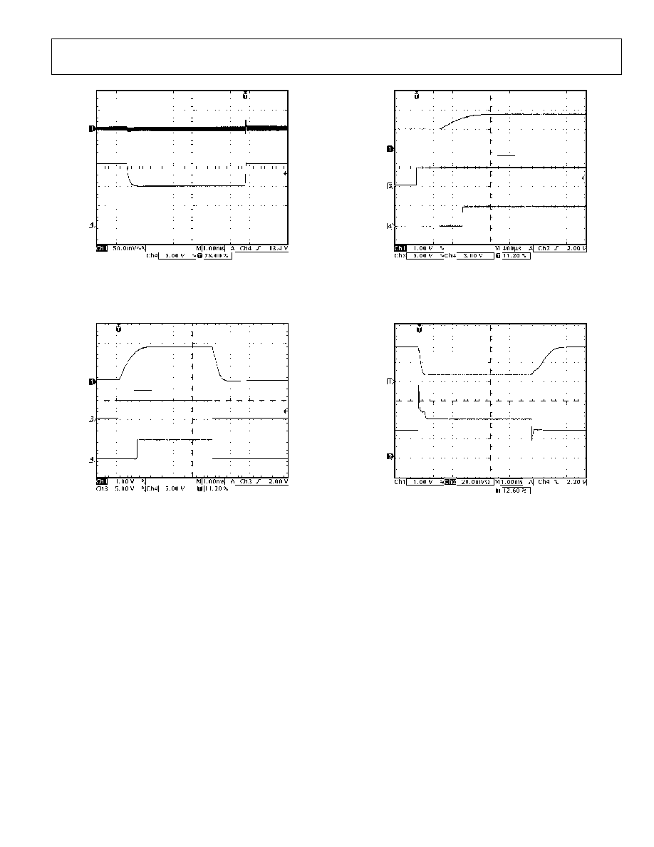
Figure 10. Load Transient Response, 1.5 A to 15 A
ADP1821
Rev. 0 | Page 9 of 20
05310-015
OUTPUT VOLTAGE
(50mV/DIV)
INPUT VOLTAGE
(5V/DIV)
Figure 11. Line Transient Response, 10 V to 16 V
05310-012
OUTPUT VOLTAGE
(1V/DIV)
SHDN (5V/DIV)
PWGD (5V/DIV)
Figure 12. Power-On Response
05310-013
OUTPUT VOLTAGE
(1V/DIV)
SHDN (5V/DIV)
PWGD (5V/DIV)
Figure 13. Power-On Response, Prebiased Output
05310-014
OUTPUT VOLTAGE
(1V/DIV)
LOAD CURRENT
(10A/DIV)
Figure 14. Output Short-Circuit Response and Recovery

ADP1821
Rev. 0 | Page 10 of 20
THEORY OF OPERATION
The ADP1821 is a versatile, economical, synchronous-rectified,
fixed-frequency, pulse width-modulated (PWM) step-down
controller capable of generating an output voltage as low as
0.6 V while sourcing up to 20 A to the load. It is ideal for a wide
range of high-power applications, such as DSP power and pro-
cessor core power in telecom, medical imaging, and indus-trial
applications. The ADP1821 controller runs from 3.0 V to 5.5 V,
and accepts a power input voltage between 1.0 V and 20 V.
The ADP1821 operates at a fixed, internally set 300 kHz or
600 kHz switching frequency that is controlled by the state of
the FREQ input. The high frequency reduces external compo-
nent size and cost while maintaining high efficiency. For noise
sensitive applications where the switching frequency needs to
be more tightly controlled, synchronize the ADP1821 to an
external signal whose frequency is between 300 kHz and
1.2 MHz.
The ADP1821 includes adjustable soft start with output reverse-
current protection, and a unique adjustable, lossless current
limit. It operates over the -40∞C to +85∞C temperature range
and is available in a space-saving, 16-lead QSOP package.
CURRENT LIMIT SCHEME
The ADP1821 employs a unique, programmable cycle-by-cycle
lossless current-sensing scheme that uses an inexpensive high-
value resistor to set the current limit. A 50 A current source is
forced out of CSL to a programming resistor connected to SW.
The resulting voltage across the current sense resistor sets the
current limit threshold. When on-state voltage of the low-side,
MOSFET synchronous rectifier exceeds the programmed
threshold, the low-side MOSFET remains on, preventing
another on cycle and reducing the inductor current. Once the
MOSFET voltage, and thus the inductor current, is below the
current-sense threshold, the synchronous rectifier is allowed to
turn off and another cycle begins.
When the ADP1821 senses an overcurrent condition, SS sinks
current from the soft-start capacitor through an internal
2.5 k resistor, reducing the voltage at SS, and thus reducing
the regulated output voltage. The ADP1821 remains in this
mode for as long as the over-current condition persists. When
the over-current condition is removed, operation resumes in
soft-start mode. This ensures that when the overload condition
is removed, the output voltage smoothly transitions back to
regulation while providing protection for overload and short-
circuit conditions.
SOFT START
When powering up or resuming operation after shutdown,
overload, or short-circuit conditions, the ADP1821 employs an
adjustable soft-start feature that reduces input current transients
and prevents output voltage overshoot at start-up and overload
conditions. The soft-start period is set by the value of the soft-
start capacitor, C
SS
, between SS and GND.
When starting the ADP1821, C
SS
is initially discharged. It is
enabled by either driving SHDN high or by bringing VCC
above the undervoltage lockout threshold. C
SS
begins charging
to 0.8 V through an internal 100 k resistor. As C
SS
charges, the
regulation voltage at FB is limited to the lesser of either the vol-
tage at SS or the internal 0.6 V reference voltage. As the voltage
at SS rises, the output voltage rises proportionally until the
voltage at SS exceeds 0.6 V. At this time, the output voltage is
regulated to the desired voltage.
If the output voltage is precharged prior to turn-on, the ADP1821
prevents reverse inductor current, which would discharge the
output voltage. Once the voltage at SS exceeds the 0.6 V regula-
tion voltage, the reverse current is re-enabled to allow the
output voltage regulation to be independent of load current.
To override the soft-start feature, leave SS unconnected. This
allows the output voltage to rise as quickly as possible and
eliminates the soft-start period.
HIGH-SIDE DRIVER (BST and DH)
Gate drive for the high-side power MOSFET is generated by a
flying capacitor boost circuit. This circuit allows the high-side,
N-channel MOSFET gate to be driven above the input voltage,
allowing full enhancement and low voltage drop across the
MOSFET. The circuit is powered from a flying capacitor from
SW to BST that in turn is powered from the PVCC gate driver
voltage. When the low-side switch is turned on, SW is driven to
PGND and the flying capacitor is charged from PVCC through
an external Schottky rectifier. The capacitor stores sufficient
charge to power BST to drive DH high and to fully enhance the
high-side, N-channel MOSFET. Use a flying capacitor value
greater than 100◊ the high-side MOSFET input capacitance.
LOW-SIDE DRIVER (DL)
DL is the gate drive for the low-side, power MOSFET synchro-
nous rectifier. Synchronous rectification reduces conduction
losses developed by a conventional rectifier by replacing it with
a low-resistance MOSFET switch. DL turns on the synchronous
rectifier by driving the gate voltage to PVCC. The MOSFET is
turned off by driving the gate voltage to PGND.

ADP1821
Rev. 0 | Page 11 of 20
An active dead time reduction circuit reduces the break-before-
make time of the switching to limit the losses due to current
flowing through the synchronous rectifier body diode or
external Schottky rectifier.
INPUT VOLTAGE RANGE
The ADP1821 takes its internal power from the VCC and
PVCC inputs. PVCC powers the low-side MOSFET gate drive
(DL) and VCC powers the internal control circuitry. Both of
these inputs are limited to between 3.0 V and 5.5 V. Bypass
PVCC to PGND with a 1 F or greater capacitor. Bypass VCC
to GND with a 0.1 F or greater capacitor.
The power input to the dc-to-dc converter can range between
1.2◊ the output voltage up to 20 V. Bypass the power input to
PGND with a suitably large capacitor. See the Selecting the
Input Capacitor section.
SETTING THE OUTPUT VOLTAGE
The output voltage is set using a resistive voltage divider from
the output to FB. The voltage divider drops the output voltage
to the 0.6 V FB regulation voltage to set the regulation output
voltage. The output voltage is set to voltages as low as 0.6 V and
as high as 85% of the minimum power input voltage (see the
Feedback Voltage Divider section).
SWITCHING FREQUENCY CONTROL
The ADP1821 has a logic controlled frequency select input,
FREQ, that sets the switching frequency to 300 kHz or 600 kHz.
Drive FREQ low for 300 kHz and drive it high for 600 kHz.
The SYNC input is used to synchronize the converter switching
frequency to an external signal. The synchronization range is
300 kHz to 1.2 MHz. The acceptable synchronization frequency
range is limited to twice the nominal switching frequency set by
FREQ. For lower frequency synchronization, between 300 kHz
and 600 kHz, connect FREQ to GND. For higher frequency
synchronization, between 480 kHz and 1.2 MHz, connect FREQ
to VCC (see the Synchronizing the Converter section for more
information).
COMPENSATION
The control loop is compensated by an external series RC net-
work from COMP to FB and sometimes requires a series RC in
parallel with the top voltage divider resistor. COMP is the
output of the internal error amplifier.
The internal error amplifier compares the voltage at FB to the
internal 0.6 V reference voltage. The difference between the two
(the feedback voltage error) is amplified by the 1,000 V-to-V
gain of the error amplifier. To optimize the ADP1821 for
stability and transient response for a given set of external
components and input/output voltage conditions, choose the
compensation components. For more information on choosing
the compensation components, see the Compensating the
Regulator section.
POWER-GOOD INDICATOR
The ADP1821 features an open-drain power-good output,
(PWGD), that sinks current when the output voltage drops
8.3% below or 25% above the nominal regulation voltage. Two
comparators measure the voltage at FB to set these thresholds.
The PWGD output also sinks current if an overtemperature or
input undervoltage conditions are detected and is operational
with VCC voltage as low as 1.0 V.
Use this output as a simple power-good signal by connecting a
pull-up resistor from PWGD to an appropriate supply voltage.
SHUTDOWN CONTROL
The ADP1821 dc-to-dc converter features a low-power shut-
down mode that reduces quiescent supply current to 1 A. To
shut down the ADP1821, drive SHDN low. To turn it on, drive
SHDN high. For automatic startup, connect SHDN to VCC.

ADP1821
Rev. 0 | Page 12 of 20
APPLICATION INFORMATION
SELECTING THE INPUT CAPACITOR
The input capacitor absorbs the switched input current of the
dc-to-dc converter, allowing the input source to deliver smooth
dc current. Choose an input capacitor whose impedance at the
switching frequency is lower than the input source impedance.
Use low equivalent series resistance (ESR) capacitors, such as
low-ESR tantalum, ceramic, or organic electrolyte types, such as
Sanyo Os-Con. For all types of capacitors, make sure that the
current rating of the capacitor is greater than 1/2 of the
maximum output load current.
OUTPUT LC FILTER
The output LC filter smoothes the switched voltage at SW
making the dc output voltage. Choose the output LC filter to
achieve the desired output ripple voltage. Since the output LC
filter is part of the regulator negative-feedback control loop, the
choice of the output LC filter components affects the regulation
control loop stability.
Choose an inductor value such that the inductor ripple current
is approximately 1/3 of the maximum dc output load current.
Using a larger value inductor results in a physical size larger
than required and using a smaller value results in increased
losses in the inductor and/or MOSFET switches.
Choose the inductor value by the following equation:
-
=
IN
OUT
OUT
L
SW
V
V
V
I
f
L
1
)
)(
(
1
(1)
where:
L is the inductor value.
f
SW
is the switching frequency.
V
OUT
is the output voltage.
V
IN
is the input voltage.
I
L
is the inductor ripple current, typically 1/3 of the maximum
dc load current.
Choose the output capacitor to set the desired output voltage
ripple. The ADP1821 functions with output capacitors that have
both high and low equivalent series resistance (ESR). For high-
ESR capacitors, such as tantalum or electrolytic types, many
parallel connected capacitors might be required to achieve the
desired output ripple voltage. When choosing an output capa-
citor, consider ripple current rating, capacitance, and ESR.
Make sure that the ripple current rating is higher than the
maximum inductor ripple current (I
L
).
The output ripple voltage is a function of the inductor ripple
current and the capacitor impedance at the switching frequency.
For high ESR capacitors, the impedance is dominated by the
ESR, while for low ESR capacitors the impedance is dominated
by the capacitance. Determine if the capacitor is high ESR or
low ESR be comparing the zero frequency formed by the
capacitance and the ESR to the switching frequency.
(
)
(
)
ESR
C
f
OUT
ESRZ
=
2
1
(2)
where:
f
ESRZ
is the frequency of the output capacitor ESR zero.
C
OUT
is the output capacitance.
ESR is the equivalent series resistance of the capacitor.
If f
ESRZ
is much less than the switching frequency, then the
capacitor is high ESR and the ESR dominates the impedance at
the switching frequency. If f
ESRZ
is much greater than the
switching frequency, the capacitor is low ESR and the
impedance is dominated by the capacitance at the switching
frequency.
When using capacitors whose impedance is dominated by ESR
at the switching frequency (such as tantalum or aluminum
electrolytic capacitors), approximate the output voltage ripple
current by the following equation:
)
(ESR
I
V
L
OUT
(3)
where:
V
OUT
is the output ripple voltage.
I
L
is the inductor ripple current.
ESR is the total equivalent series resistance of the output
capacitor (or the parallel combination of ESR of all parallel-
connected output capacitors).
Make sure that the ripple current rating of the output capaci-
tor(s) is greater than the maximum inductor ripple current.
For output capacitors whose ESR is much lower than the capa-
citive impedance at the switching frequency, the capacitive
impedance dominates the output ripple current. In this case,
determine the ripple voltage by the following equation:
(
)
( )
SW
OUT
L
OUT
f
C
I
V
8
(4)
where:
f
SW
is the switching frequency.
C
OUT
is the output capacitance.
When f
ESRZ
is approximately the same as the switch-ing
frequency, the square-root sum of the squares of the two ripples
applies or
[
]
(
)( )
2
2
8
)
(
+
SW
OUT
L
L
OUT
f
C
I
ESR
I
V
(5)

ADP1821
Rev. 0 | Page 13 of 20
SELECTING THE MOSFETS
The choice of MOSFET directly affects the dc-to-dc converter
performance. The MOSFET must have low on resistance to
reduce I
2
R losses and low gate-charge to reduce transition
losses. Also, the MOSFET must have low thermal resistance to
ensure that the power dissipated in the MOSFET does not result
in excessive MOSFET die temperature.
The high-side MOSFET carries the load current during on-time
and carries all the transitions losses of the converter. Typically,
the lower the MOSFET on resistance, the higher the gate charge
and vice versa. Therefore, it is important to choose a high-side
MOSFET that balances the two losses. The conduction loss of
the high-side MOSFET is determined by the equation
(
)( )
IN
OUT
ON
LOAD
C
V
V
R
I
P
(6)
where:
P
C
= conduction power loss.
R
ON
= MOSFET on resistance.
The transition loss is approximated by the equation
(
)( )( )( )
SW
G
IN
LOAD
T
f
Q
V
I
P
(7)
where:
P
T
= transition loss power.
Q
G
= MOSFET total gate charge.
f
SW
= converter switching frequency.
The total power dissipation of the high-side MOSFET is the
sum of the two losses or
( )( )
T
C
HS
P
P
P
(8)
where P
HS
is the total high-side, MOSFET power loss.
The low-side MOSFET does not carry the transition losses and
carries the inductor current when the high-side MOSFET is off.
For high input voltage and low output voltage, the low-side
MOSFET carries the current most of the time, and therefore to
achieve high efficiency it is critical to optimize the low-side
MOSFET for low on resistance. In cases where the power loss
exceeds the MOSFET rating or lower resistance is required than
is available in a single MOSFET, connect multiple low-side
MOSFETs in parallel. The equation for low-side MOSFET
power loss is
(
) ( )
-
IN
OUT
ON
LOAD
LS
V
V
R
I
P
1
2
(9)
where:
P
LS
is the low-side MOSFET on resistance.
R
ON
is the total on resistance of the low-side MOSFET(s).
If multiple low-side MOSFETs are used in parallel, use the
parallel combination of the on resistances for determining R
ON
to solve this equation.
SETTING THE CURRENT LIMIT
The internal current limit circuit measures the voltage across
the low-side MOSFET to determine the load current. When the
low-side MOSFET current exceeds the current limit, the high-
side MOSFET is not allowed to turn on until the current drops
below the current limit.
The current limit is set through the current limit resistor, R
CL
.
The current sense pin, CSL, sources 50 A through R
CL
. This
creates an offset voltage of resistance of R
CL
multiplied by the
50 A CSL current. When the low-side MOSFET voltage is
equal to or greater than the offset voltage, the ADP1821 is in
current limit mode and prevents additional on-time cycles.
Choose the current limit resistor by the equation
(
)
(
)
A
R
I
R
ONWC
LPK
CL
=
42
(10)
where:
I
LPK
is the peak inductor current.
R
ONWC
is the worst-case (maximium) low-side MOSFET on
resistance.
The worst-case, low-side, MOSFET on resistance can be found
in the MOSFET data sheet. Note that MOSFETs typically
increase on resistance with increasing die temperature. To
determine the worst-case MOSFET on resistance, calculate the
worst-case MOSFET temperature (based on the MOSFET
power loss) and multiply by the ratio between the typical on
resistance at that temperature and the on resistance at 25∞C, as
listed in the MOSFET data sheet.
FEEDBACK VOLTAGE DIVIDER
The output regulation voltage is set through the feedback vol-
tage divider. The output voltage is reduced through the voltage
divider and drives the FB feedback input. The regulation
threshold at FB is 0.6 V. For the low-side resistor of the voltage
divider, R
BOT
, use 10 k. A larger value resistor can be used, but
results in a reduction in output voltage accuracy. Choose RTOP
to set the output voltage by the following equation:
=
FB
FB
OUT
BOT
TOP
V
V
V
R
R
_
(11)
where:
R
TOP
is the high-side voltage divider resistance.
R
BOT
is the low-side voltage divider resistance.
V
OUT
is the regulated output voltage.
V
FB
is the feedback regulation threshold, 0.6 V.

ADP1821
Rev. 0 | Page 14 of 20
COMPENSATING THE REGULATOR
The output of the error amplifier at COMP is used to compen-
sate the regulation control system. Connect a resistor capacitor,
RC, and network from COMP to FB to compensate the
regulator.
The first step in selecting the compensation components is
determining the desired regulation control crossover frequency,
f
CO
. Choose a crossover frequency approximately 1/10 of the
switching frequency, or
10
SW
CO
f
f
=
(12)
The characteristics of the output capacitor affects the compen-
sation required to stabilize the regulator. The output capacitor
acts with its equivalent series resistance (ESR) to form a zero.
Calculate the ESR zero frequency by the following equation:
(
)
(
)
ESR
C
f
OUT
ESRZ
=
2
1
(13)
Note that as similar capacitors are placed in parallel, the ESR
zero frequency remains the same.
If
2
CO
ESRZ
f
f
, use the ESR zero to stabilize the regulator (see
the Compensation Using the ESR Zero section). If
, use a feed-forward network to stabilize the
regulator (see the
CO
ESRZ
f
f
2
Compensation Using Feed Forward section).
If
CO
ESRZ
CO
f
f
f
2
2
, use both the ESR zero and feed-forward
zeros to stabilize the regulator (see the Compensation Using
Both the ESR and Feed-Forward Zeros section).
In all three cases, although not required, it is sometimes
beneficial to add an additional compensation capacitor, C
C2
,
from COMP to FB to reduce high frequency noise. This
capacitor forms an extra pole in the loop response. Choose this
capacitor such that the pole occurs at approximately 1/2 of the
switching frequency or
( )(
)
COMP
C
SW
PC
R
C
f
F
2
2
2
1
2
=
=
(14)
Solving for C
C2
,
( )(
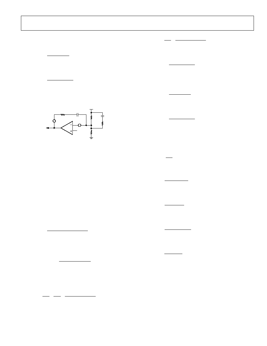
Compensation Using the ESR Zero
V
OUT
TO
PWM
COMP
FB
0.6V
R
COMP
C
COMP
R
TOP
R
BOT
05310-003
INTERNAL ERROR AMPLIFIER
Figure 15. Compensation Using the ESR Zero
If the output capacitor ESR zero is sufficiently low (less-than-or-
equal-to Ω of the crossover frequency), use the ESR to stabilize
the regulator. In this case, use the circuit shown in Figure 17.
Choose the compensation resistor to set the desired crossover
frequency, typically 1/10 of the switching frequency or
(
)
(
)
(
)( )
( )
2
LC
IN
CO
ZESR
RAMP
TOP
COMP
f
V
f
f
V
R
R
=
(16)
where:
R
COMP
is the compensation resistor.
V
RAMP
is the internal ramp peak voltage, 1.25 V.
f
ZESR
and
f
CO
are the ESR zero and crossover frequencies.
V
IN
is the dc input voltage.
f
LC
is the characteristic frequency of the output LC filter or
LC
f
LC
=
2
1
(17)
using known constants
(
)(
)
( )
( )
( )
IN
SW
ZESR
TOP
COMP
V
C
L
f
f
R
R
9
.
4
(18)
Choose the compensation capacitor to set the compensation
zero, f
ZC
, to the lesser of 1/4 of the crossover frequency or 1/2 of
the LC resonant frequency or
(
)(
)
COMP
COMP
SW
CO
ZC
R
C
f
f
f
=
=
=
2
1
20
4
(19)
or
(
)(
)
COMP
COMP
LC
ZC
R
C
f
f
=
=
2
1
2
(20)
)
COMP
SW
C
R
f
C
=
2
2
2
(15)
Solving for C
COMP
,
( )(
)
COMP
CO
COMP
R
f
C
=
2
4
(21)
ADP1821
Rev. 0 | Page 15 of 20
)
In terms of the switching frequency and combining the
constants,
( )(
COMP
SW
COMP
R
f
C
37
.
6
(22)
or
( )(
)
COMP
LC
COMP
R
f
C
=
2
2
(23)
or whichever is greater.
Compensation Using Feed Forward
V
OUT
TO
PWM
COMP
FB
0.6V
R
COMP
C
COMP
R
TOP
R
BOT
R
FF
C
FF
05310-004
INTERNAL ERROR AMPLIFIER
Figure 16. Compensation Using Feed Forward
If the ESR zero is at too high a frequency to be useful in stabili-
zing the regulator, add a series RC network (as shown in
Figure 16) in parallel with the topside voltage divider resistor,
R
TOP
. This adds an additional zero and pole pair that is used to
increase the phase at crossover, thus improving stability.
Choose the feed-forward zero frequency for 1/7 of the crossover
frequency and the feed-forward pole at 7◊ the crossover
frequency. This sets the ratio of pole-to-zero frequency of
approximately 50:1 for optimum stability.
Choose the compensation resistor, R
COMP
, to set the crossover
frequency by the following equation:
(
)
(
)( )( )
( )
2
LC
IN
CO
ZFF
RAMP
TOP
COMP
f
V
f
f
V
R
R
=
(24)
where f
ZFF
is the feed-forward zero frequency and is 1/7 of the
crossover frequency. Simplifying the following equation:
(
)
( )
( )
( )
IN
SW
TOP
COMP
V
C
L
f
R
R
2
0705
.
0
(25)
Choose the compensation capacitor to set the compensation
zero, f
ZC
, to the lesser of 1/4 of the crossover frequency or 1/2 of
the LC resonant frequency or
(
)(
)
COMP
COMP
SW
CO
ZC
R
C
f
f
f
=
=
=
2
1
20
4
(26)
or
(
)(
)
COMP
COMP
LC
ZC
R
C
f
f
=
=
2
1
2
(27)
Solving for C
COMP
,
( )(
)
COMP
CO
COMP
R
f
C
=
2
4
(28)
In terms of the switching frequency and combining the
constants,
( )(
)
COMP
SW
COMP
R
f
C
37
.
6
(29)
or
( )(
)
COMP
LC
COMP
R
f
C
=
2
2
(30)
or whichever is greater.
Choose the feed-forward capacitor, C
FF
, to set the feed-forward
zero at 1/7 of the crossover frequency
7
CO
ZFF
f
f
=
(31)
or
(
)
( )
FF
TOP
CO
C
R
f
=
2
7
(32)
Simplifying and solving for C
FF
,
(
)
( )
SW
TOP
FF
f
R
C
14
.
11
=
(33)
Choose the feed-forward resistor, R
FF
, to set the condition
( )
( )( )
FF
FF
CO
C
R
f
=
2
7
1
(34)
Simplifying and solving for R
FF
,
( )( )
FF
SW
FF
C
f
R
227
.
0
=
(35)
Compensation Using Both the ESR and Feed-Forward
Zeros
If the output capacitor ESR zero frequency falls between 1/2 of
the crossover frequency to 2◊ the crossover frequency, use the
circuit shown in Figure 17, such that the ESR zero along with a
feed-forward network stabilizes the regulator. In this case, the
feed-forward zero is set to 1/7 of the crossover frequency and
the feed-forward pole is set to the same frequency as the ESR
zero.

ADP1821
Rev. 0 | Page 16 of 20
Choose the compensation resistor, R
COMP
, to set the crossover
frequency by the following equation:
(
)(
)(
)
( )
( )
2
LC
IN
CO
ZFF
RAMP
TOP
COMP
f
V
f
f
V
R
R
=
(36)
where f
ZFF
is the feed-forward zero frequency and is 1/7 of the
crossover frequency. Simplifying the following equation:
(
)
( )
( )
( )
IN
SW
TOP
COMP
V
C
L
f
R
R
2
0705
.
0
(37)
Choose the compensation capacitor to set the compensation
zero, f
ZC
, to Ω of the LC resonant frequency or
(
)(
)
COMP
COMP
LC
ZC
R
C
f
f
=
=
2
1
2
(38)
Solving for C
COMP
,
( )(
)
COMP
LC
COMP
R
f
C
=
2
2
(39)
Choose the feed-forward capacitor, C
FF
, to set the feed-forward
zero at 1/7 of the crossover frequency
7
CO
ZFF
f
f
=
(40)
or
(
)
( )
FF
TOP
CO
C
R
f
=
2
7
(41)
Simplifying and solving for C
FF
,
(
)
( )
SW
TOP
FF
f
R
C
14
.
11
=
(42)
Choose the feed-forward resistor, R
FF
, to set the condition
( )
( )( )
FF
FF
CO
C
R
f
=
2
7
1
(43)
Simplifying and solving for R
FF
,
( )
( )
FF
SW
FF
C
f
R
227
.
0
=
(44)
SETTING THE SOFT START PERIOD
The ADP1821 uses an adjustable soft start to limit the output
voltage ramp-up period, limiting the input inrush current. The
soft start is set by selecting the capacitor, C
SS
, from SS to GND.
The ADP1823 charges C
SS
to 0.8 V through an internal resistor.
The voltage on C
SS
while it is charging is
-
=
SS
RC
t
CSS
e
V
V
1
8
.
0
(45)
where R is the internal 100 k resistor. The soft-start period, t
SS
,
is achieved when V
CSS
= 0.6 V or
-
=
)
(
100
1
8
.
0
6
.
0
SS
SS
C
k
t
e
V
V
(46)
or
( )
386
.
1
8
.
0
6
.
0
1
1
100
=
-
-
=
V
V
n
C
k
t
SS
SS
(47)
Solving for C
SS
and combining constants,
SS
SS
t
C
)
10
213
.
7
(
6
-
◊
=
(48)
SYNCHRONIZING THE CONVERTER
The dc-to-dc converter switching can be synchronized to an
external signal. This allows multiple ADP1821 converters to be
operated at the same frequency to prevent frequency beating or
other interactions.
To synchronize the ADP1821 switching to an external signal,
drive the sync input with the synchronizing signal. The
ADP1821 can only synchronize up to 2◊ the nominal oscillator
frequency. If the frequency is set to 300 kHz (FREQ connected
to GND), it can synchronize up to 600 kHz. If the frequency is
set to 600 kHz (FREQ connected to VCC), it can synchronize to
1.2 MHz.
The high-side MOSFET turn-on follows the rising edge of the
sync input by approximately 320 ns. To prevent erratic switch-
ing frequency make sure that the falling edge of the sync input
signal does not coincide with the falling edge of the dc-dc
converter switching or
(
)
( )
[
]
IN
OUT
SW
SYNC
V
V
f
ns
D
+
320
(49)
where:
D
SYNC
is the duty cycle of the synchronization waveform.
f
SW
is the synchronized switching frequency.
Make sure that in all combinations of frequency, input, and
output voltages that the sync input fall time does not align with
the dc-to-dc converter fall time.
ADP1821
Rev. 0 | Page 17 of 20
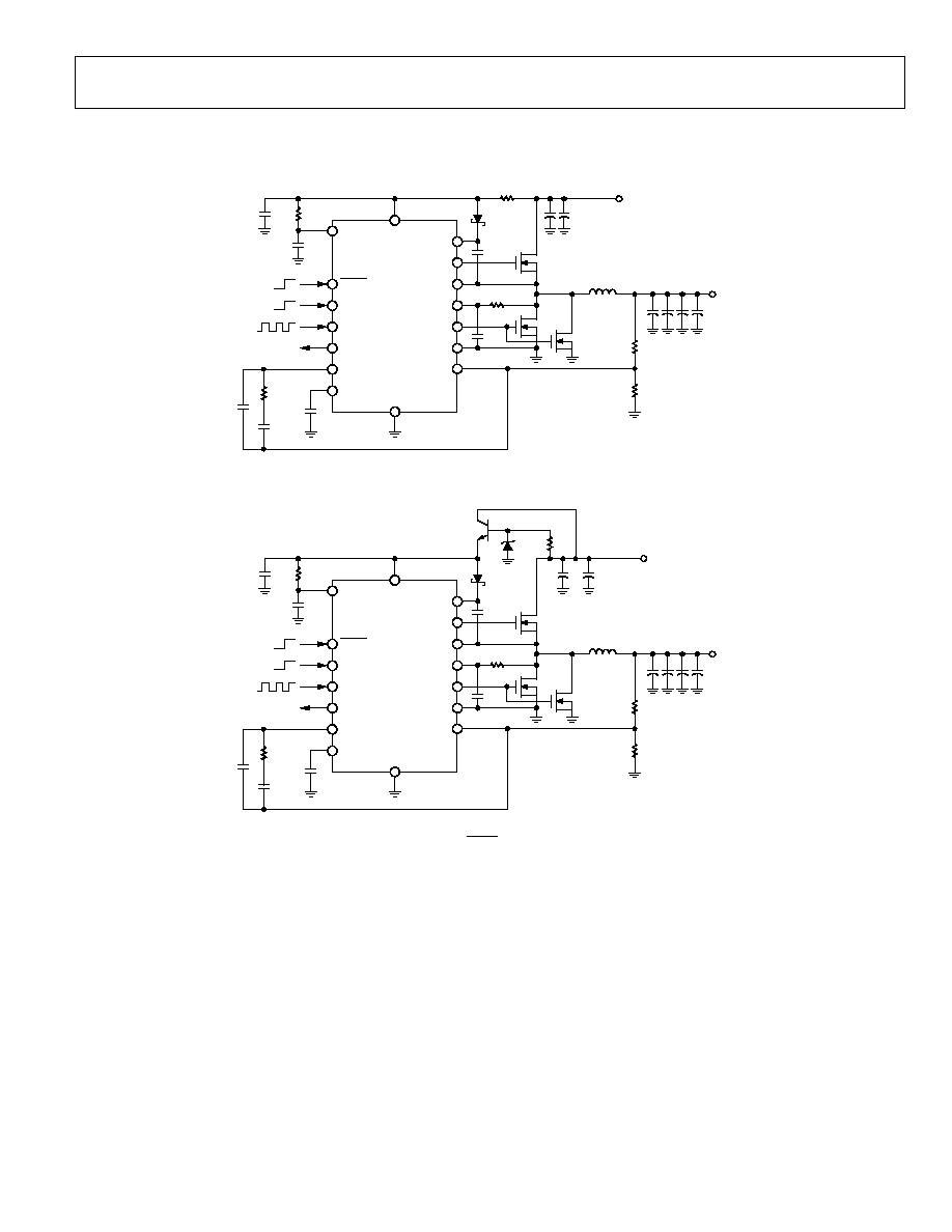
APPLICATION CIRCUITS
VCC
PVCC
GND
1
F
10
100nF
ADP1821
2
◊
IRF3711
IRF3711
1
H
2
◊
180
F
20V
INPUT
5V
4
◊
1000
F, 4V
OUTPUT
1.8V, 15A
0.1
F
2.2pF
6.18k
05310-020
80.6k
15pF
1
F
CMOSH-3
390pF
20k
10k
10
FREQ
SYNC
PWGD
COMP
SS
BST
DH
SW
CSL
DL
PGND
FB
SHDN
Figure 17. Typical Application Circuit, 5 V Input
VCC
PVCC
GND
1
F
10
100nF
ADP1821
2
◊
IRF3711
IRF3711
1
H
2
◊
180
F
20V
INPUT
12V
4
◊
1000
F, 4V
OUTPUT
1.8V, 15A
0.1
F
2.2pF
6.18k
05310-021
80.6k
15pF
1
F
CMOSH-3
390pF
20k
10k
CMOZ5V6
1.2k
CMST2222A
FREQ
SYNC
PWGD
COMP
SS
BST
DH
SW
CSL
DL
PGND
FB
SHDN
Figure 18. Typical Application Circuit, 12 V Input,
FREQ = SYNC = GND, SHDN = VCC, 5 A Load Current,
T
A
= 25∞C, Unless Otherwise Specified
ADP1821
Rev. 0 | Page 18 of 20
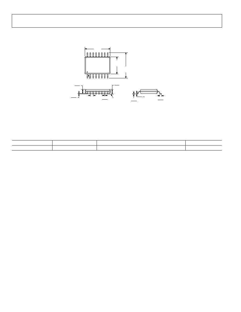
OUTLINE DIMENSIONS
COMPLIANT TO JEDEC STANDARDS MO-137-AB
16
9
8
1
PIN 1
SEATING
PLANE
0.010
0.004
0.012
0.008
0.025
BSC
0.010
0.006
0.050
0.016
8∞
0∞
COPLANARITY
0.004
0.065
0.049
0.069
0.053
0.154
BSC
0.236
BSC
0.193
BSC
Figure 19. 16-Lead Shrink Small Outline Package [QSOP]
(RQ-16)
Dimensions shown in inches
ORDERING GUIDE
Model
Temperature Range
Package Description
Package Option
ADP1821ARQZ-R7
1
≠40∞C to +85∞C
16-Lead Shrink Small Outline Package [QSOP]
RQ-16
1
Z = Pb-free part.

ADP1821
Rev. 0 | Page 19 of 20
NOTES

ADP1821
Rev. 0 | Page 20 of 20
NOTES
© 2005 Analog Devices, Inc. All rights reserved. Trademarks and registered
trademarks are the property of their respective owners.
D05310≠0≠7/05(0)