 | –≠–ª–µ–∫—Ç—Ä–æ–Ω–Ω—ã–π –∫–æ–º–ø–æ–Ω–µ–Ω—Ç: ADP2107 | –°–∫–∞—á–∞—Ç—å:  PDF PDF  ZIP ZIP |
Document Outline
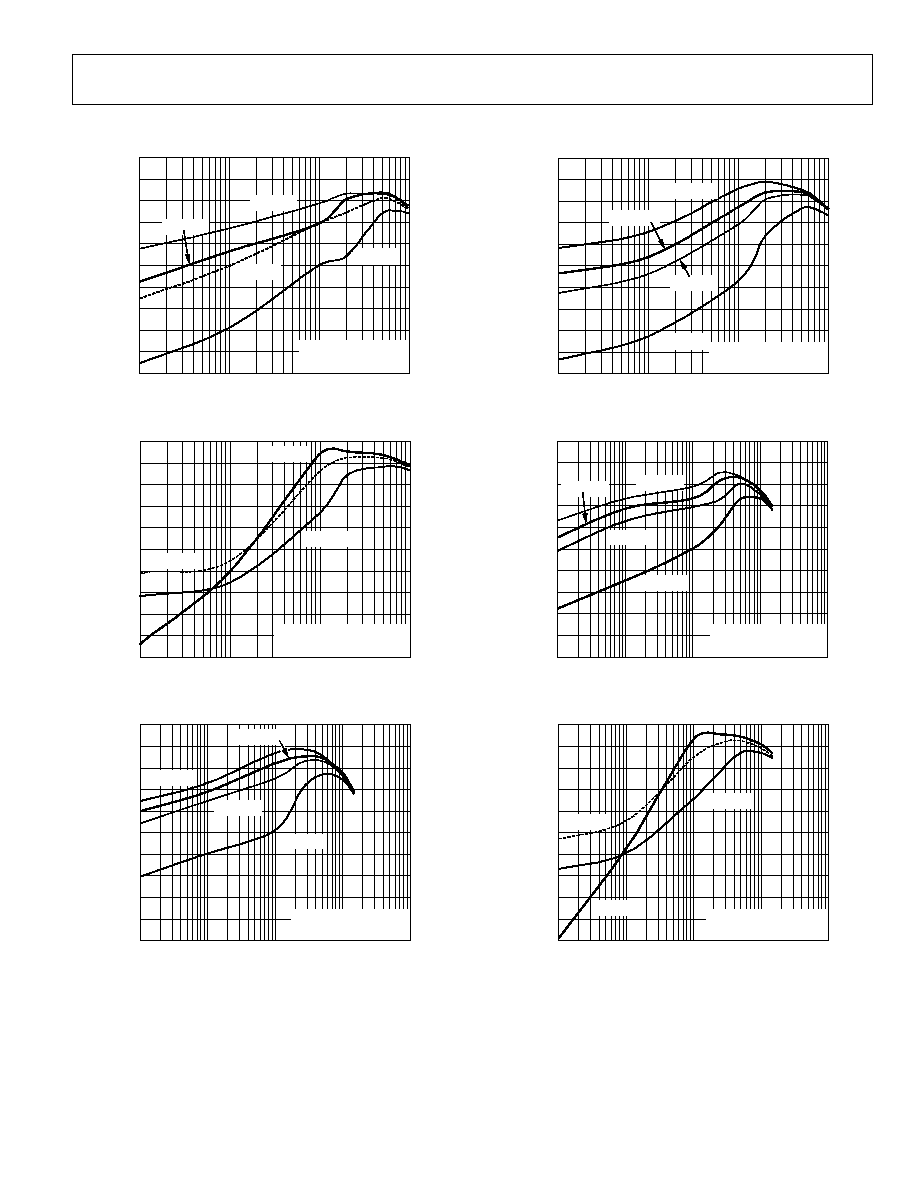
- ˛ˇ
- ˛ˇ
- ˛ˇ
- ˛ˇ
- ˛ˇ
- ˛ˇ
- ˛ˇ
- ˛ˇ
- ˛ˇ
- ˛ˇ
- ˛ˇ
- ˛ˇ
- ˛ˇ
- ˛ˇ
- ˛ˇ
- ˛ˇ
- ˛ˇ
- ˛ˇ
- ˛ˇ
- ˛ˇ
- ˛ˇ
- ˛ˇ
- LOAD TRANSIENT RESPONSE
- ˛ˇ
- ˛ˇ
- DESIGN EXAMPLE
- ˛ˇ
- ˛ˇ
- ˛ˇ
- ˛ˇ
- ˛ˇ

1 Amp/1.5 Amp/2 Amp Synchronous,
Step-Down DC-to-DC Converters
ADP2105/ADP2106/ADP2107
Rev. 0
Information furnished by Analog Devices is believed to be accurate and reliable. However, no
responsibility is assumed by Analog Devices for its use, nor for any infringements of patents or other
rights of third parties that may result from its use. Specifications subject to change without notice. No
license is granted by implication or otherwise under any patent or patent rights of Analog Devices.
Trademarks and registered trademarks are the property of their respective owners.
One Technology Way, P.O. Box 9106, Norwood, MA 02062-9106, U.S.A.
Tel: 781.329.4700
www.analog.com
Fax: 781.461.3113
©2006 Analog Devices, Inc. All rights reserved.
FEATURES
Extremely high 97% efficiency
Ultralow quiescent current: 20 A
1.2 MHz switching frequency
0.1 A shutdown supply current
Maximum load current:
ADP2105: 1 A
ADP2106: 1.5 A
ADP2107: 2 A
Input voltage: 2.7 V to 5.5 V
Output voltage: 0.8 V to V
IN
Maximum duty cycle: 100%
Smoothly transitions into low dropout (LDO) mode
Internal synchronous rectifier
Small 16-lead 4 mm ◊ 4 mm LFCSP_VQ package
Optimized for small ceramic output capacitors
Enable/Shutdown logic input
Undervoltage lockout
Soft start
APPLICATIONS
Mobile handsets
PDAs and palmtop computers
Telecommunication/Networking equipment
Set top boxes
Audio/Video consumer electronics
GENERAL DESCRIPTION
The ADP2105/ADP2106/ADP2107 are low quiescent current,
synchronous, step-down dc-to-dc converters in a compact 4 mm ◊
4 mm LFCSP_VQ package. At medium-to-high load currents,
these devices use a current-mode, constant-frequency pulse
width modulation (PWM) control scheme for excellent stability
and transient response. To ensure the longest battery life in
portable applications, the ADP2105/ADP2106/ADP2107 use a
pulse frequency modulation (PFM) control scheme under light
load conditions that reduces switching frequency to save power.
The ADP2105/ADP2106/ADP2107 run from input voltages of
2.7 V to 5.5 V, allowing single Li+/Li- polymer cell, multiple
alkaline/NiMH cells, PCMCIA, and other standard power sources.
The output voltage of ADP2105/ADP2106/ADP2107-ADJ is
adjustable from 0.8 V to the input voltage, while the ADP2105/
ADP2106/ADP2107-xx are available in preset output voltage
options of 3.3 V, 1.8 V, 1.5 V, and 1.2 V. Each of these variations is
available in three maximum current levels, 1 A (ADP2105), 1.5 A
(ADP2106), and 2 A (ADP2107). The power switch and synchro-
nous rectifier are integrated for minimal external part count
and high efficiency. During logic-controlled shutdown, the
input is disconnected from the output, and it draws less than
0.1 A from the input source. Other key features include
undervoltage lockout to prevent deep-battery discharge and
programmable soft start to limit inrush current at startup.
TYPICAL PERFORMANCE CHARACTERISTICS
100
75
0
2000
0
607
9-
0
01
LOAD CURRENT (mA)
EF
F
I
C
I
EN
C
Y
(%
)
95
90
85
80
200
400
600
800 1000 1200 1400 1600 1800
V
IN
= 3.3V
V
IN
= 3.6V
V
IN
= 5V
V
OUT
= 2.5V
Figure 1. Efficiency vs. Load Current for the ADP2107 with V
OUT
= 2.5 V
TYPICAL OPERATING CIRCUIT
ADP2107-ADJ
OFF
EN
SS
LX2
FB
PWIN1
AGND
OUTPUT VOLTAGE = 2.5V
COMP
ON
PGND
IN
GND
GND
GND
NC
GND
LX1
PWIN2
V
IN
V
IN
INPUT VOLTAGE = 2.7V TO 5.5V
10F
FB
1nF
70k
120pF
1
2
3
4
12
11
10
9
16
15
14
13
5
6
7
8
2H
4.7F
LOAD
0A TO 2A
10F
10F
10
0.1F
NC = NO CONNECT
060
79
-
0
02
85k
40k
FB
Figure 2. Circuit Configuration of ADP2107 with V
OUT
= 2.5 V

ADP2105/ADP2106/ADP2107
Rev. 0 | Page 2 of 32
TABLE OF CONTENTS
Features .............................................................................................. 1
Applications....................................................................................... 1
General Description ......................................................................... 1
Typical Performance Characteristics ............................................. 1
Typical Operating Circuit................................................................ 1
Revision History ............................................................................... 2
Specifications..................................................................................... 3
Absolute Maximum Ratings............................................................ 5
Thermal Resistance ...................................................................... 5
Boundary Condition .................................................................... 5
ESD Caution.................................................................................. 5
Pin Configuration and Function Descriptions............................. 6
Typical Performance Characteristics ............................................. 7
Theory of Operation ...................................................................... 12
Control Scheme .......................................................................... 12
PWM Mode Operation.............................................................. 12
PFM Mode Operation................................................................ 12
Pulse-Skipping Threshold ......................................................... 12
100% Duty Cycle Operation (LDO Mode) ............................. 12
Slope Compensation .................................................................. 13
Features ........................................................................................ 13
Applications Information .............................................................. 15
External Component Selection................................................. 15
Setting the Output Voltage........................................................ 15
Inductor Selection ...................................................................... 16
Output Capacitor Selection....................................................... 17
Input Capacitor Selection.......................................................... 17
Input Filter................................................................................... 18
Soft Start ...................................................................................... 18
Loop Compensation .................................................................. 18
Bode Plots.................................................................................... 19
Load Transient Response .......................................................... 20
Efficiency Considerations ......................................................... 21
Thermal Considerations............................................................ 21
Design Example.......................................................................... 22
External Component Recommendations.................................... 24
Circuit Board Layout Recommendations ................................... 26
Evaluation Board ............................................................................ 27
Evaluation Board Schematic (ADP2107-1.8V)...................... 27
Recommended PCB Board Layout
(Evaluation Board Layout)........................................................ 27
Application Circuits ....................................................................... 29
Outline Dimensions ....................................................................... 31
Ordering Guide .......................................................................... 31
REVISION HISTORY
7/06--Revision 0: Initial Version

ADP2105/ADP2106/ADP2107
Rev. 0 | Page 3 of 32
SPECIFICATIONS
V
IN
=
3.6 V @ T
A
= 25∞C, unless otherwise noted.
1
Bold values indicate -40∞C T
J
+125∞C.
Table 1.
Parameter Conditions
Min
Typ
Max
Unit
INPUT CHARACTERISTICS
Input Voltage Range
2.7
5.5 V
Undervoltage Lockout Threshold
V
IN
rising
2.2
2.4
2.6
V
V
IN
falling
2.0
2.2
2.5
V
Undervoltage Lockout Hysteresis
2
200
mV
OUTPUT CHARACTERISTICS
Output Regulation Voltage
ADP210x-3.3, load = 10 mA
3.267
3.3
3.333
V
ADP210x-3.3,
V
IN
= 3.5 V to 5.5 V, no load to full load
3.201
3.3
3.399
V
ADP210x-1.8, load = 10 mA
1.782
1.8
1.818
V
ADP210x-1.8,
V
IN
= 2.7 V to 5.5 V, no load to full load
1.746
1.8
1.854
V
ADP210x-1.5, load = 10 mA
1.485
1.5
1.515
V
ADP210x-1.5,
V
IN
= 2.7 V to 5.5 V, no load to full load
1.455
1.5
1.545
V
ADP210x-1.2, load = 10 mA
1.188
1.2
1.212
V
ADP210x-1.2,
V
IN
= 2.7 V to 5.5 V, no load to full load
1.164
1.2
1.236
V
Load Regulation
ADP2105
0.4
%/A
ADP2106
0.5
%/A
ADP2107
0.6
%/A
Line Regulation
3
Measured in servo loop
0.1 0.3 %/V
Output Voltage Range
ADP210x-ADJ
0.8
V
IN
V
FEEDBACK CHARACTERISTICS
ADP210x-1.2
3
6
A
ADP210x-1.5
4
8
A
ADP210x-1.8
5
10
A
OUT_SENSE Bias Current
ADP210x-3.3
10
20
A
FB Regulation Voltage
ADP210x-ADJ
0.784
0.8
0.816
V
FB Bias Current
ADP210x-ADJ
-0.1
+0.1
A
INPUT CURRENT CHARACTERISTICS
IN Operating Current
ADP210x-ADJ, V
FB
= 0.9 V
20
30
A
ADP210x-xx, output voltage 10% above regulation voltage
20
30
A
IN Shutdown Current
V
EN
= 0 V
0.1
1
5
A
LX (SWITCH NODE) CHARACTERISTICS
LX On Resistance
4
P-channel switch
100
165
m
N-channel synchronous rectifier
90
140
m
LX Leakage Current
4
V
IN
= 5.5 V, V
LX
= 0 V, 5.5 V
0.1
1
5
A
LX Peak Current Limit
4
P-channel switch, ADP2107
2.6
2.9
3.3
A
P-channel switch, ADP2106
2.0
2.25
2.6
A
P-channel switch, ADP2105
1.3
1.5
1.8
A
LX Minimum On-Time
4
In PWM mode of operation, V
IN
= 5.5 V
100
ns
ENABLE CHARACTERISTICS
EN Input High Voltage
V
IN
= 2.7 V to 5.5 V
2 V
EN Input Low Voltage
V
IN
= 2.7 V to 5.5 V
0.4
V
EN Input Leakage Current
V
IN
= 5.5 V, V
EN
= 0 V, 5.5 V
-1 -0.1
+1
A
OSCILLATOR FREQUENCY
V
IN
= 2.7 V to 5.5 V
1
1.2
1.4
MHz
SOFT START PERIOD
C
SS
= 1 nF
750
1000
1200
s

ADP2105/ADP2106/ADP2107
Rev. 0 | Page 4 of 32
Parameter Conditions
Min
Typ
Max
Unit
THERMAL CHARACTERISTICS
Thermal Shutdown Threshold
140
∞C
Thermal Shutdown Hysteresis
40
∞C
COMPENSATOR TRANSCONDUCTANCE (G
m
)
50
A/V
ADP2105
1.875
A/V
ADP2106
2.8125
A/V
CURRENT SENSE AMPLIFIER GAIN (G
CS
)
2
ADP2107
3.625
A/V
1
All limits at temperature extremes are guaranteed via correlation using standard statistical quality control (SQC). Typical values are at T
A
= 25∞C.
2
Guaranteed by design.
3
The ADP2015/ADP2106/ADP2107 line regulation was measured in a servo loop on the ATE that adjusts the feedback voltage to achieve a specific comp voltage.
4
All LX (switch node) characteristics are guaranteed only when the LX1 and LX2 pins are tied together.
5
These specifications are guaranteed from -40∞C to +85∞C.

ADP2105/ADP2106/ADP2107
Rev. 0 | Page 5 of 32
ABSOLUTE MAXIMUM RATINGS
Table 2.
Parameter Rating
IN, EN, SS, COMP, OUT_SENSE/FB to
AGND
-0.3 V to +6 V
LX1, LX2 to PGND
-0.3 V to (V
IN
+ 0.3 V)
PWIN1, PWIN2 to PGND
-0.3 V to +6 V
PGND to AGND
-0.3 V to +0.3 V
GND to AGND
-0.3 V to +0.3 V
PWIN1, PWIN2 to IN
-0.3 V to +0.3 V
Operating Junction Temperature Range
-40∞C to +125∞C
Storage Temperature Range
-65∞C to +150∞C
Soldering Conditions
JEDEC J-STD-020
Stresses above those listed under Absolute Maximum Ratings
may cause permanent damage to the device. This is a stress
rating only; functional operation of the device at these or any
other conditions above those indicated in the operational
section of this specification is not implied. Exposure to absolute
maximum rating conditions for extended periods may affect
device reliability.
THERMAL RESISTANCE
JA
is specified for the worst-case conditions, that is, a device
soldered in a circuit board for surface-mount packages.
Table 3. Thermal Resistance
Package Type
JA
1
Unit
16-Lead LFCSP_VQ/QFN
40
∞C/W
Maximum Power Dissipation
1
W
1
JA
is specified for the worst-case conditions; that is,
JA
is specified for device
soldered in circuit board for surface mount packages.
BOUNDARY CONDITION
Natural convection, 4-layer board, exposed pad soldered to
the PCB.
ESD CAUTION
ESD (electrostatic discharge) sensitive device. Electrostatic charges as high as 4000 V readily accumulate on the
human body and test equipment and can discharge without detection. Although this product features
proprietary ESD protection circuitry, permanent damage may occur on devices subjected to high energy
electrostatic discharges. Therefore, proper ESD precautions are recommended to avoid performance
degradation or loss of functionality.

ADP2105/ADP2106/ADP2107
Rev. 0 | Page 6 of 32
PIN CONFIGURATION AND FUNCTION DESCRIPTIONS
PIN 1
INDICATOR
NC = NO CONNECT
11 PGND
12 LX2
10 LX1
9
PWIN2
C
O
M
P
5
S
S
6
A
G
N
D
7
N
C
8
ADP2105/
ADP2106/
ADP2107
TOP VIEW
(Not to Scale)
15
G
N
D
1
6
O
U
T
_
SEN
SE/
F
B
14
I
N
13
P
W
I
N
1
EN 1
GND 2
GND 3
GND 4
0
60
79
-
0
03
Figure 3. Pin Configuration
Table 4. Pin Function Descriptions
Mnemonic
Pin No.
ADP210x-xx
ADP210x-ADJ
Description
1 EN
EN
Enable Input. Drive EN high to turn on the ADP2105/ADP2106/ADP2107. Drive EN low to turn
it off and reduce the input current to 0.1
A.
2, 3, 4,
15
GND GND Test Pins. These pins are used by Analog Devices, Inc. for internal testing and are not ground
return pins. Tie these pins to the AGND plane as close to the ADP2105/ADP2106/ADP2107 as
possible.
5 COMP COMP
Feedback Loop Compensation Node. COMP is the output of the internal transconductance
error amplifier. Place a series RC network from COMP to AGND to compensate the converter.
See the Loop Compensation section.
6 SS
SS
Soft Start Input. Place a capacitor from SS to AGND to set the soft start period. A 1 nF capacitor
sets a 1 ms soft start period.
7 AGND AGND
Analog Ground. Connect the ground of the compensation components, soft start capacitor,
and the voltage divider on the FB pin to the AGND pin as close as possible to the ADP2105/
ADP2106/ADP2107. Also connect AGND to the exposed pad of ADP2105/ADP2106/ADP2107.
8
NC
NC
No Connect. Not internally connected. Can be connected to other pins or left unconnected.
9, 13
PWIN2,
PWIN1
PWIN2, PWIN1
Power Source Inputs. The source of the PFET high-side switch. Bypass each PWIN pin to the nearest
PGND plane with a 4.7 F or greater capacitor as close as possible to the ADP2105/ADP2106/
ADP2107. See the Input Capacitor Selection section.
10, 12
LX1, LX2
LX1, LX2
Switch Outputs. The drain of the P-channel power switch and N-channel synchronous rectifier.
Tie the two LX pins together and connect the output LC filter between LX and the output
voltage.
11 PGND
PGND
Power Ground. Connect the ground return of all input and output capacitors to PGND pin,
using a power ground plane as close as possible to the ADP2105/ADP2106/ADP2107. Also
connect PGND to the exposed pad of the ADP2105/ADP2106/ADP2107.
14 IN
IN
ADP2105/ADP2106/ADP2107 Power Input. The power source for the ADP2105/ADP2106/
ADP2107 internal circuitry. Connect IN and PWIN1 with a 10 resistor as close as possible to
the ADP2105/ADP2106/ADP2107. Bypass IN to AGND with a 0.1 F or greater capacitor. See
the Input Filter section.
16 OUT_SENSE
FB
Output Voltage Sense or Feedback Input. For fixed output versions, connect OUT_SENSE to the
output voltage. For adjustable versions, FB is the input to the error amplifier. Drive FB through
a resistive voltage divider to set the output voltage. The FB regulation voltage is 0.8 V.
ADP2105/ADP2106/ADP2107
Rev. 0 | Page 7 of 32
TYPICAL PERFORMANCE CHARACTERISTICS
100
50
1
1000
0
607
9-
0
04
LOAD CURRENT (mA)
EF
F
I
C
I
EN
C
Y
(%
)
10
100
95
90
85
80
75
70
65
60
55
V
IN
= 5.5V
V
IN
= 4.2V
V
IN
= 3.6V
V
IN
= 2.7V
INDUCTOR: SD14, 2.5µH
DCR: 60m
T
A
= 25∞C
Figure 4. Efficiency--ADP2105 (1.2 V Output)
100
50
1
1000
06
07
9-
05
2
LOAD CURRENT (mA)
EF
F
I
C
I
EN
C
Y (
%
)
10
100
95
90
85
80
75
70
65
60
55
V
IN
= 4.2V
V
IN
= 5.5V
V
IN
= 3.6V
INDUCTOR: CDRH5D18, 4.1H
DCR: 43m
T
A
= 25∞C
Figure 5. Efficiency--ADP2105 (3.3 V Output)
100
50
1
10000
06
07
9-
06
2
LOAD CURRENT (mA)
EF
F
I
C
I
EN
C
Y (
%
)
95
90
85
80
75
70
65
60
55
10
100
1000
V
IN
= 2.7V
V
IN
= 3.6V
V
IN
= 4.2V
V
IN
= 5.5V
INDUCTOR: D62LCB, 2µH
DCR: 28m
T
A
= 25∞C
Figure 6. Efficiency--ADP2106 (1.8 V Output)
100
50
1
1000
06
07
9-
06
1
LOAD CURRENT (mA)
EF
F
I
C
I
EN
C
Y (
%
)
10
100
95
90
85
80
75
70
65
60
55
V
IN
= 2.7V
V
IN
= 3.6V
V
IN
= 4.2V
V
IN
= 5.5V
INDUCTOR: SD3814, 3.3µH
DCR: 93m
T
A
= 25∞C
Figure 7. Efficiency--ADP2105 (1.8 V Output)
100
50
1
10000
0
607
9-
0
08
LOAD CURRENT (mA)
EF
F
I
C
I
EN
C
Y
(%
)
95
90
85
80
75
70
65
60
55
10
100
1000
V
IN
= 5.5V
V
IN
= 4.2V
V
IN
= 3.6V
V
IN
= 2.7V
INDUCTOR: D62LCB, 2µH
DCR: 28m
T
A
= 25∞C
Figure 8. Efficiency--ADP2106 (1.2 V Output)
100
50
1
10000
06
07
9-
05
3
LOAD CURRENT (mA)
EF
F
I
C
I
EN
C
Y (
%
)
95
90
85
80
75
70
65
60
55
10
100
1000
V
IN
= 4.2V
V
IN
= 5.5V
V
IN
= 3.6V
INDUCTOR: D62LCB, 3.3µH
DCR: 47m
T
A
= 25∞C
Figure 9. Efficiency--ADP2106 (3.3 V Output)

ADP2105/ADP2106/ADP2107
Rev. 0 | Page 8 of 32
100
50
1
10000
0
607
9-
0
10
LOAD CURRENT (mA)
EF
F
I
C
I
EN
C
Y
(%
)
95
90
85
80
75
70
65
60
55
10
100
1000
V
IN
= 4.2V
V
IN
= 5.5V
V
IN
= 3.6V
V
IN
= 2.7V
INDUCTOR: SD12, 1.2µH
DCR: 37m
T
A
= 25∞C
Figure 10. Efficiency--ADP2107 (1.2 V)
100
50
1
10000
06
07
9-
05
4
LOAD CURRENT (mA)
EF
F
I
C
I
EN
C
Y (
%
)
95
90
85
80
75
70
65
60
55
10
100
1000
V
IN
= 4.2V
V
IN
= 5.5V
V
IN
= 3.6V
INDUCTOR: CDRH5D28, 2.5µH
DCR: 13m
T
A
= 25∞C
Figure 11. Efficiency--ADP2107 (3.3 V)
1.85
1.75
0.1
10000
06
07
9-
0
64
LOAD CURRENT (mA)
OU
TP
U
T
V
O
L
T
A
G
E
(
V
)
5.5V, ≠40∞C
5.5V, +25∞C
2.7V, ≠40∞C
2.7V, +25∞C
2.7V, +125∞C
3.6V, ≠40∞C
3.6V, +25∞C
3.6V, +125∞C
5.5V, +125∞C
1.83
1.81
1.79
1.77
1
10
100
1000
Figure 12. Output Voltage Accuracy--ADP2107 (1.8 V)
100
50
1
10000
06
07
9-
06
3
LOAD CURRENT (mA)
EF
F
I
C
I
EN
C
Y (
%
)
95
90
85
80
75
70
65
60
55
10
100
1000
V
IN
= 2.7V
V
IN
= 3.6V
V
IN
= 4.2V
V
IN
= 5.5V
INDUCTOR: D62LCB, 1.5µH
DCR: 21m
T
A
= 25∞C
Figure 13. Efficiency--ADP2107 (1.8 V)
1.23
1.17
0.01
10000
06
07
9-
0
82
LOAD CURRENT (mA)
OU
TP
U
T
V
O
L
T
A
G
E
(
V
)
5.5V, ≠40∞C
5.5V, +25∞C
2.7V, ≠40∞C
2.7V, +25∞C
2.7V, +125∞C
3.6V, ≠40∞C
3.6V, +25∞C
3.6V, +125∞C
5.5V, +125∞C
0.1
1
10
100
1000
1.22
1.21
1.20
1.19
1.18
Figure 14. Output Voltage Accuracy--ADP2107 (1.2 V)
3.38
3.22
0.01
10000
06
07
9-
0
81
LOAD CURRENT (mA)
OU
TP
U
T
V
O
L
T
A
G
E
(
V
)
0.1
1
10
100
1000
3.36
3.34
3.32
3.30
3.28
3.26
3.24
5.5V, ≠40∞C
5.5V, +25∞C
3.6V, ≠40∞C
3.6V, +25∞C
3.6V, +125∞C
5.5V, +125∞C
Figure 15. Output Voltage Accuracy--ADP2107 (3.3 V)
ADP2105/ADP2106/ADP2107
Rev. 0 | Page 9 of 32
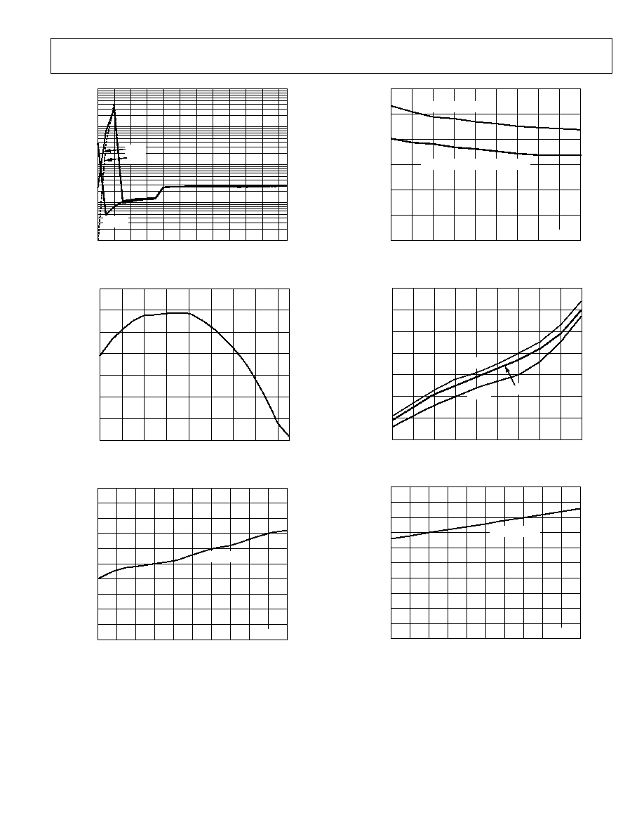
10000
1
0.8
0
607
9-
0
16
INPUT VOLTAGE (V)
I
NP
U
T
CUR
RE
NT
(
µ
A)
10
100
1000
1.2
1.6
2.0
2.4
2.8
3.2
3.6
4.0
4.4
4.8
5.2
≠40∞C
+125∞C
+25∞C
Figure 16. Quiescent Current vs. Input Voltage
≠40
125
06
07
9-
01
7
TEMPERATURE (∞C)
F
E
E
D
B
A
C
K
VO
L
T
A
G
E (
V)
≠20
0
20
40
60
80
100
120
0.795
0.796
0.797
0.798
0.799
0.800
0.801
0.802
Figure 17. Feedback Voltage vs. Temperature
1.75
1.25
0
607
9-
0
73
2.7
5.7
INPUT VOLTAGE (V)
P
E
AK
C
URRE
NT
L
I
M
I
T
(
A)
1.70
1.65
1.60
1.55
1.50
1.45
1.40
1.35
1.30
3.0
3.3
3.6
3.9
4.2
4.5
4.8
5.1
5.4
ADP2105 (1A)
T
A
= 25∞C
Figure 18. Peak Current Limit of ADP2105
120
0
2.7
5.4
0
607
9-
0
18
INPUT VOLTAGE (V)
S
W
O
N
R
ESI
S
T
A
N
C
E (
m
)
100
80
60
40
20
3.0
3.3
3.6
3.9
4.2
4.5
4.8
5.1
NMOS SYNCHRONOUS RECTIFIER
PMOS POWER SWITCH
T
A
= 25∞C
Figure 19. Switch On Resistance vs. Input Voltage
1260
1190
2.7
5.4
0
607
9-
0
21
INPUT VOLTAGE (V)
S
W
I
T
C
HI
NG
F
RE
Q
UE
NCY
(
k
Hz
)
1250
1240
1230
1220
1210
1200
3.0
3.3
3.6
3.9
4.2
4.5
4.8
5.1
≠40∞C
+25∞C
+125∞C
Figure 20. Switching Frequency vs. Input Voltage
2.35
1.85
0
607
9-
0
72
2.7
5.7
INPUT VOLTAGE (V)
P
E
AK
C
URRE
NT
L
I
M
I
T
(
A)
2.30
2.25
2.20
2.15
2.10
2.05
2.00
1.95
1.90
3.0
3.3
3.6
3.9
4.2
4.5
4.8
5.1
5.4
ADP2106 (1.5A)
T
A
= 25∞C
Figure 21. Peak Current Limit of ADP2106

ADP2105/ADP2106/ADP2107
Rev. 0 | Page 10 of 32
3.00
2.50
0
607
9-
0
71
2.7
5.7
INPUT VOLTAGE (V)
P
E
AK
C
URRE
NT
L
I
M
I
T
(
A)
2.95
2.90
2.85
2.80
2.75
2.70
2.65
2.60
2.55
3.0
3.3
3.6
3.9
4.2
4.5
4.8
5.1
5.4
ADP2107 (2A)
T
A
= 25∞C
Figure 22. Peak Current Limit of ADP2107
150
0
0
607
9-
0
67
2.7
5.7
INPUT VOLTAGE (V)
P
UL
S
E
S
KI
P
P
I
N
G
T
HRE
S
HO
L
D CURRE
NT
(
m
A)
3.0
3.3
3.6
3.9
4.2
4.5
4.8
5.1
5.4
135
120
105
90
75
60
45
30
15
V
OUT
= 2.5V
V
OUT
= 1.2V
V
OUT
= 1.8V
T
A
= 25∞C
Figure 23. Pulse Skipping Threshold vs. Input Voltage for ADP2106
06
07
9-
07
4
4
3
1
LX NODE (SWITCH NODE)
OUTPUT VOLTAGE
INDUCTOR CURRENT
: 260mV
@: 3.26V
CH1
1V
45.8%
CH4 1A
CH3 5V
M 10µs
A CH1
1.78V
T
Figure 24. Short Circuit Response at Output
135
0
2.7
5.7
0
607
9-
0
66
INPUT VOLTAGE (V)
P
U
L
S
E
S
KI
P
P
I
NG
T
HRE
S
HO
L
D CURR
E
NT
(
m
A)
120
105
90
75
60
45
30
15
3.0
3.3
3.6
3.9
4.2
4.5
4.8
5.1
5.4
V
OUT
= 1.8V
V
OUT
= 1.2V
V
OUT
= 2.5V
T
A
= 25∞C
Figure 25. Pulse Skipping Threshold vs. Input Voltage for ADP2105
195
0
0
607
9-
0
68
2.7
5.7
INPUT VOLTAGE (V)
P
UL
S
E
S
KI
P
P
I
N
G
T
HRE
S
HO
L
D CURRE
NT
(
m
A)
3.0
3.3
3.6
3.9
4.2
4.5
4.8
5.1
5.4
180
165
150
135
120
105
90
75
60
45
30
15
V
OUT
= 2.5V
V
OUT
= 1.8V
V
OUT
= 1.2V
T
A
= 25∞C
Figure 26. Pulse Skipping Threshold vs. Input Voltage for ADP2107
≠40
06
07
9-
0
83
JUNCTION TEMPERATURE (∞C)
S
W
I
T
CH O
N RE
S
I
S
T
ANCE
(
m
)
≠20
0
20
40
60
80
100
120
0
20
40
60
80
100
120
140
PMOS POWER SWITCH
NMOS SYNCHRONOUS RECTIFIER
Figure 27. Switch On Resistance vs. Temperature
ADP2105/ADP2106/ADP2107
Rev. 0 | Page 11 of 32
06
07
9-
03
0
CH1
50mV
6%
CH4 200mA
CH3 2V
M 2µs
A CH3
3.88V
T
3
4
1
INDUCTOR CURRENT
OUTPUT VOLTAGE (AC-COUPLED)
LX NODE
(SWITCH NODE)
06
07
9-
03
1
CH1
20mV
17.4%
CH4 1A
CH3 2V
M 1µs
A CH3
3.88V
T
3
4
1
LX NODE (SWITCH NODE)
OUTPUT VOLTAGE (AC-COUPLED)
INDUCTOR CURRENT
Figure 28. PFM Mode of Operation at Very Light Load (10 mA)
Figure 31. PWM Mode of Operation at Medium/Heavy Load (1.5 A)
06
07
9-
03
3
CH1
50mV
17.4%
CH4 200mA
CH3 2V
M 400ns
A CH3
3.88V
T
3
4
1
LX NODE (SWITCH NODE)
OUTPUT VOLTAGE (AC-COUPLED)
INDUCTOR CURRENT
06
07
9-
03
2
CH1
1V
45%
CH4 1A
CH3 5V
M 4µs
A CH3
1.8V
T
3
4
1
INDUCTOR CURRENT
OUTPUT VOLTAGE
CHANNEL 3
FREQUENCY
= 336.6kHz
: 2.86A
@: 2.86A
LX NODE (SWITCH NODE)
Figure 29. DCM Mode of Operation at Light Load (100 mA)
Figure 32. Current Limit Behavior of ADP2107 (Frequency Foldback)
06
07
9-
03
4
CH1
20mV
13.4%
CH4 1A
CH3 2V
M 2µs
A CH3
1.84V
T
3
4
1
LX NODE (SWITCH NODE)
OUTPUT VOLTAGE (AC-COUPLED)
INDUCTOR CURRENT
06
07
9-
03
5
CH1
1V
20.2%
CH4 500mA
CH3 5V
M 400µs
A CH1
1.84V
T
3
4
1
ENABLE VOLTAGE
INDUCTOR CURRENT
OUTPUT VOLTAGE
Figure 30. Minimum Off Time Control at Dropout
Figure 33. Startup and Shutdown Waveform (C
SS
= 1 nF
SS Time = 1 ms)

ADP2105/ADP2106/ADP2107
Rev. 0 | Page 12 of 32
THEORY OF OPERATION
The ADP2105/ADP2106/ADP2107 are step-down, dc-to-dc
converters that use a fixed frequency, peak current-mode
architecture with an integrated high-side switch and low-side
synchronous rectifier. The high 1.2 MHz switching frequency
and tiny 16-lead, 4 mm ◊ 4 mm LFCSP_VQ package allow for
a small step-down dc-to-dc converter solution. The integrated
high-side switch (P-channel MOSFET) and synchronous rectifier
(N-channel MOSFET) yield high efficiency at medium-to-
heavy loads. Light load efficiency is improved by smoothly
transitioning to variable frequency PFM mode.
The ADP2105/ADP2106/ADP2107-ADJ operate with an input
voltage from 2.7 V to 5.5 V and regulate an output voltage down
to 0.8 V. The ADP2105/ADP2106/ADP2107 are also available with
preset output voltage options of 3.3 V, 1.8 V, 1.5 V, and 1.2 V.
CONTROL SCHEME
The ADP2105/ADP2106/ADP2107 operate with a fixed
frequency, peak current-mode PWM control architecture at
medium-to-high loads for high efficiency, but shift to a variable
frequency PFM control scheme at light loads for lower quies-
cent current. When operating in fixed frequency PWM mode,
the duty cycle of the integrated switches is adjusted to regulate
the output voltage, but when operating in PFM mode at light
loads, the switching frequency is adjusted to regulate the output
voltage.
The ADP2105/ADP2106/ADP2107 operate in the PWM mode
only when the load current is greater than the pulse-skipping
threshold current. At load currents below this value, the converter
smoothly transitions to the PFM mode of operation.
PWM MODE OPERATION
In PWM mode, the ADP2105/ADP2106/ADP2107 operate at
a fixed frequency of 1.2 MHz set by an internal oscillator. At the
start of each oscillator cycle, the P-channel MOSFET switch is
turned on, putting a positive voltage across the inductor. Current
in the inductor increases until the current sense signal crosses
the peak inductor current level that turns off the P-channel
MOSFET switch and turns on the N-channel MOSFET synchro-
nous rectifier. This puts a negative voltage across the inductor,
causing the inductor current to decrease. The synchronous
rectifier stays on for the rest of the cycle, unless the inductor
current reaches zero, which causes the zero-crossing comparator
to turn off the N-channel MOSFET, as well. The peak inductor
current is set by the voltage on the COMP pin. The COMP pin
is the output of a transconductance error amplifier that compares
the feedback voltage with an internal 0.8 V reference.
PFM MODE OPERATION
The ADP2105/ADP2106/ADP2107 smoothly transition to the
variable frequency PFM mode of operation when the load current
decreases below the pulse-skipping threshold current, switching
only as necessary to maintain the output voltage within regulation.
When the output voltage dips below regulation, the ADP2105/
ADP2106/ADP2107 enter PWM mode for a few oscillator cycles
to increase the output voltage back to regulation. During the wait
time between bursts, both power switches are off, and the output
capacitor supplies all the load current. Because the output voltage
dips and recovers occasionally, the output voltage ripple in this
mode is larger than the ripple in the PWM mode of operation.
PULSE-SKIPPING THRESHOLD
The output current at which the ADP2105/ADP2106/ADP2107
transition from variable frequency PFM control to fixed frequency
PWM control is called the pulse-skipping threshold. The pulse-
skipping threshold has been optimized for excellent efficiency
over all load currents. The variation of pulse-skipping threshold
with input voltage and output voltage is shown in Figure 23,
Figure 25, and Figure 26.
100% DUTY CYCLE OPERATION (LDO MODE)
As the input voltage drops, approaching the output voltage,
the ADP2105/ADP2106/ADP2107 smoothly transition to 100%
duty cycle, maintaining the P-channel MOSFET switch on continu-
ously. This allows the ADP2105/ADP2106/ADP2107 to regulate
the output voltage until the drop in input voltage forces the
P-channel MOSFET switch to enter dropout, as shown in the
following equation:
V
IN(MIN)
= I
OUT
◊ (R
DS(ON) - P
+ DCR
IND
) + V
OUT(NOM)
The ADP2105/ADP2106/ADP2107 achieve 100% duty cycle
operation by stretching the P-channel MOSFET switch on-time
if the inductor current does not reach the peak inductor current
level by the end of the clock cycle. Once this happens, the oscil-
lator remains off until the inductor current reaches the peak
inductor current level, at which time the switch is turned off and
the synchronous rectifier is turned on for a fixed off-time. At
the end of the fixed off-time, another cycle is initiated. As the
ADP2105/ADP2106/ADP2107 approach dropout, the switching
frequency decreases gradually to smoothly transition to 100%
duty cycle operation.

ADP2105/ADP2106/ADP2107
Rev. 0 | Page 13 of 32
SLOPE COMPENSATION
Slope compensation stabilizes the internal current control loop
of the ADP2105/ADP2106/ADP2107 when operating beyond
50% duty cycle to prevent sub-harmonic oscillations. It is imple-
mented by summing a fixed scaled voltage ramp to the current
sense signal during the on-time of the P-channel MOSFET switch.
The slope compensation ramp value determines the minimum
inductor that can be used to prevent sub-harmonic oscillations
at a given output voltage. The slope compensation ramp values
for ADP2105/ADP2106/ADP2107 follow. For more information,
see the Inductor Selection section.
For the ADP2105:
Slope Compensation Ramp Value = 0.72 A/s
For the ADP2106:
Slope Compensation Ramp Value = 1.07 A/s
For the ADP2107:
Slope Compensation Ramp Value = 1.38 A/s
FEATURES
Enable/Shutdown
Drive EN high to turn on the ADP2105/ADP2106/ADP2107.
Drive EN low to turn off the ADP2105/ADP2106/ADP2107,
reducing input current below 0.1 A. To force the ADP2105/
ADP2106/ADP2107 to automatically start when input power
is applied, connect EN to IN. When shut down, the ADP2105/
ADP2106/ADP2107 discharge the soft start capacitor, causing
a new soft start cycle every time they are re-enabled.
Synchronous Rectification
In addition to the P-channel MOSFET switch, the ADP2105/
ADP2106/ADP2107 include an integrated N-channel MOSFET
synchronous rectifier. The synchronous rectifier improves
efficiency, especially at low output voltage, and reduces cost and
board space by eliminating the need for an external rectifier.
Current Limit
The ADP2105/ADP2106/ADP2107 have protection circuitry to
limit the direction and amount of current flowing through the
power switch and synchronous rectifier. The positive current
limit on the power switch limits the amount of current that can
flow from the input to the output, while the negative current
limit on the synchronous rectifier prevents the inductor current
from reversing direction and flowing out of the load.
Short Circuit Protection
The ADP2105/ADP2106/ADP2107 include frequency foldback
to prevent output current run-away on a hard short. When the
voltage at the feedback pin falls below 0.3 V, indicating the possi-
bility of a hard short at the output, the switching frequency is
reduced to 1/4 of the internal oscillator frequency. The reduction
in the switching frequency gives more time for the inductor to
discharge, preventing a runaway of output current.
Undervoltage Lockout (UVLO)
To protect against deep battery discharge, undervoltage lockout
circuitry is integrated on the ADP2105/ADP2106/ADP2107.
If the input voltage drops below the 2.2 V UVLO threshold, the
ADP2105/ADP2106/ADP2107 shut down, and both the power
switch and synchronous rectifier turn off. Once the voltage rises
again above the UVLO threshold, the soft start period is initiated,
and the part is enabled.
Thermal Protection
In the event that the ADP2105/ADP2106/ADP2107 junction
temperatures rise above 140∞C, the thermal shutdown circuit turns
off the converter. Extreme junction temperatures can be the
result of high current operation, poor circuit board design, and/or
high ambient temperature. A 40∞C hysteresis is included so that
when thermal shutdown occurs, the ADP2105/ADP2106/
ADP2107 do not return to operation until the on-chip tempera-
ture drops below 100∞C. When coming out of thermal
shutdown, soft start is initiated.
Soft Start
The ADP2105/ADP2106/ADP2107 include soft start circuitry
to limit the output voltage rise time to reduce inrush current at
startup. To set the soft start period, connect the soft start
capacitor (C
SS
) from SS to AGND. When the ADP2105/ADP2106/
ADP2107 are disabled, or if the input voltage is below the under-
voltage lockout threshold, C
SS
is internally discharged. When the
ADP2105/ADP2106/ADP2107 are enabled, C
SS
is charged through
an internal 0.8 A current source, causing the voltage at SS to rise
linearly. The output voltage rises linearly with the voltage at SS.

ADP2105/ADP2106/ADP2107
Rev. 0 | Page 14 of 32
1
FB FOR ADP210x-ADJ (ADJUSTABLE VERSION) AND OUT_SENSE FOR ADP210x-xx (FIXED VERSION).
14
13
9
IN
PWIN1
PWIN2
12
10
LX2
11
PGND
LX1
2
GND
7
AGND
16
OUT_SENSE
1
16
FB
1
6
SS
5
COMP
3
GND
4
GND
8
NC
15
GND
1
EN
SOFT
START
REFERENCE
0.8V
GM ERROR
AMP
FOR PRESET
VOLTAGES
OPTIONS ONLY
PWM/
PFM
CONTROL
CURRENT
LIMIT
ZERO CROSS
COMPARATOR
THERMAL
SHUTDOWN
CURRENT SENSE
AMPLIFIER
DRIVER
AND
ANTI-
SHOOT
THROUGH
SLOPE
COMPENSATION
OSCILLATOR
06
07
9-
0
37
Figure 34. Block Diagram of the ADP2105/ADP2106/ADP2107
ADP2105/ADP2106/ADP2107
Rev. 0 | Page 15 of 32
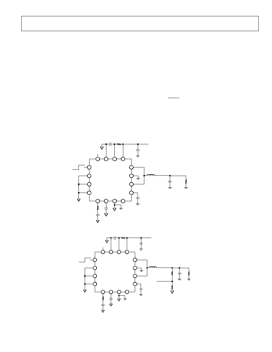
APPLICATIONS INFORMATION
EXTERNAL COMPONENT SELECTION
The external component selection for the ADP2105/ADP2106/
ADP2107 application circuits shown in Figure 35 and Figure 36
depend on input voltage, output voltage, and load current
requirements. Additionally, tradeoffs between performance
parameters like efficiency and transient response can be made
by varying the choice of external components.
SETTING THE OUTPUT VOLTAGE
The output voltage of ADP2105/ADP2106/ADP2107-ADJ is
externally set by a resistive voltage divider from the output
voltage to FB. The ratio of the resistive voltage divider sets the
output voltage, while the absolute value of those resistors sets
the divider string current. For lower divider string currents, the
small 10 nA (0.1 A maximum) FB bias current should be taken
into account when calculating resistor values. The FB bias
current can be ignored for a higher divider string current, but
this degrades efficiency at very light loads.
To limit output voltage accuracy degradation due to FB bias
current to less than 0.05% (0.5% maximum), ensure that the
divider string current is greater than 20 A. To calculate the
desired resistor values, first determine the value of the bottom
divider string resistor, R
BOT
, by
STRING
FB
BOT
I
V
R
=
where:
V
FB
= 0.8 V, the internal reference.
I
STRING
is the resistor divider string current.
OFF
EN
SS
LX2
AGND
OUTPUT VOLTAGE = 1.2V, 1.5V, 1.8V, 3.3V
COMP
ON
PGND
GND
GND
GND
NC
LX1
PWIN2
V
IN
V
IN
INPUT VOLTAGE = 2.7V TO 5.5V
V
OUT
C
SS
R
COMP
C
COMP
1
2
3
4
12
11
10
9
16
15
14
13
5
6
7
8
L
C
OUT
LOAD
C
IN2
C
IN1
10
0.1F
NC = NO CONNECT
ADP2105/
ADP2106/
ADP2107
06
07
9-
06
5
V
OUT
OUT_SENSE
PWIN1
IN
GND
Figure 35. Typical Applications Circuit for Fixed Output Voltage Options (ADP2105/ADP2106/ADP2107-xx)
OFF
EN
SS
LX2
FB
PWIN1
AGND
OUTPUT VOLTAGE
= 0.8V TO V
IN
COMP
ON
PGND
IN
GND
GND
GND
NC
GND
LX1
PWIN2
V
IN
V
IN
INPUT VOLTAGE = 2.7V TO 5.5V
FB
C
SS
R
COMP
C
COMP
1
2
3
4
12
11
10
9
16
15
14
13
5
6
7
8
L
C
OUT
LOAD
C
IN2
C
IN1
10
0.1F
R
TOP
R
BOT
FB
NC = NO CONNECT
ADP2105/
ADP2106/
ADP2107
06
07
9-
0
38
Figure 36. Typical Applications Circuit for Adjustable Output Voltage Option (ADP2105/ADP2106/ADP2107-ADJ)

ADP2105/ADP2106/ADP2107
Rev. 0 | Page 16 of 32
Once R
BOT
is determined, calculate the value of the top resistor,
R
TOP
, by
-
=
FB
FB
OUT
BOT
TOP
V
V
V
R
R
The ADP2105/ADP2106/ADP2107-xx (where xx represents
the fixed output voltage) include the resistive voltage divider
internally, reducing the external circuitry required. Connect the
OUT_SENSE to the output voltage as close as possible to the
load for improved load regulation.
INDUCTOR SELECTION
The high switching frequency of ADP2105/ADP2106/ADP2107
allows for minimal output voltage ripple even with small inductors.
The sizing of the inductor is a trade-off between efficiency and
transient response. A small inductor leads to larger inductor
current ripple that provides excellent transient response but
degrades efficiency. Due to the high switching frequency of
ADP2105/ADP2106/ADP2107, shielded ferrite core inductors
are recommended for their low core losses and low EMI.
As a guideline, the inductor peak-to-peak current ripple, I
L
,
is typically set to 1/3 of the maximum load current for optimal
transient response and efficiency.
3
)
(
)
(MAX
LOAD
SW
IN
OUT
IN
OUT
L
I
L
f
V
V
V
V
I
◊
◊
-
◊
=
H
)
(
5
.
2
)
(MAX
LOAD
IN
OUT
IN
OUT
IDEAL
I
V
V
V
V
L
◊
-
◊
◊
=
where f
SW
is the switching frequency (1.2 MHz).
The ADP2105/ADP2106/ADP2107 use slope compensation in
the current control loop to prevent subharmonic oscillations
when operating beyond 50% duty cycle. The fixed slope compen-
sation limits the minimum inductor value as a function of
output voltage.
For the ADP2105:
L > (1.12 H/V) ◊ V
OUT
For the ADP2106:
L > (0.83 H/V) ◊ V
OUT
For the ADP2107:
L > (0.66 H/V) ◊ V
OUT
Also, 4.7 H or larger inductors are not recommended because
they may cause instability in discontinuous conduction mode
under light load conditions.
Finally, it is important that the inductor be capable of handling
the maximum peak inductor current, I
PK
, determined by the
following equation:
+
=
2
)
(
L
MAX
LOAD
PK
I
I
I
Ensure that the maximum rms current of the inductor is greater
than the maximum load current, and the saturation current of
the inductor is greater than the peak current limit of the converter
used in the application.
Table 5. Minimum Inductor Value for Common Output
Voltage Options for the ADP2105 (1 A)
V
IN
V
OUT
2.7 V
3.6 V
4.2 V
5.5 V
1.2 V
1.67 H
2.00 H
2.14 H
2.35 H
1.5 V
1.68 H
2.19 H
2.41 H
2.73 H
1.8 V
2.02 H
2.25 H
2.57 H
3.03 H
2.5 V
2.80 H
2.80 H
2.80 H
3.41 H
3.3 V
3.70 H
3.70 H
3.70 H
3.70 H
Table 6. Minimum Inductor Value for Common Output
Voltage Options for the ADP2106 (1.5 A)
V
IN
V
OUT
2.7 V
3.6 V
4.2 V
5.5 V
1.2 V
1.11 H
2.33 H
2.43 H
1.56 H
1.5 V
1.25 H
1.46 H
1.61 H
1.82 H
1.8 V
1.49 H
1.50 H
1.71 H
2.02 H
2.5 V
2.08 H
2.08 H
2.08 H
2.27 H
3.3 V
2.74 H
2.74 H
2.74 H
2.74 H
Table 7. Minimum Inductor Value for Common Output
Voltage Options for the ADP2107 (2 A)
V
IN
V
OUT
2.7 V
3.6 V
4.2 V
5.5 V
1.2 V
0.83 H
1.00 H
1.07 H
1.17 H
1.5 V
0.99 H
1.09 H
1.21 H
1.36 H
1.8 V
1.19 H
1.19 H
1.29 H
1.51 H
2.5 V
1.65 H
1.65 H
1.65 H
1.70 H
3.3 V
2.18 H
2.18 H
2.18 H
2.18 H
Table 8. Inductor Recommendations for the ADP2105/
ADP2106/ADP2107
Vendor
Small-Sized Inductors
( < 5 mm ◊ 5 mm)
Large-Sized Inductors
( > 5 mm ◊ 5 mm)
Sumida
CDRH2D14, 3D16,
3D28
CDRH4D18, 4D22,
4D28, 5D18, 6D12
Toko
1069AS-DB3018,
1098AS-DE2812,
1070AS-DB3020
D52LC, D518LC,
D62LCB
Coilcraft
LPS3015, LPS4012,
DO3314
DO1605T
Cooper
Bussmann
SD3110, SD3112,
SD3114, SD3118,
SD3812, SD3814
SD10, SD12, SD14, SD52

ADP2105/ADP2106/ADP2107
Rev. 0 | Page 17 of 32
OUTPUT CAPACITOR SELECTION
The output capacitor selection affects both the output voltage
ripple and the loop dynamics of the converter. For a given loop
crossover frequency (the frequency at which the loop gain
drops to 0 dB), the maximum voltage transient excursion
(overshoot) is inversely proportional to the value of the output
capacitor. Therefore, larger output capacitors result in improved
load transient response. To minimize the effects of the dc-to-dc
converter switching, the crossover frequency of the compensation
loop should be less than 1/10 of the switching frequency. Higher
crossover frequency leads to faster settling time for a load transient
response, but it can also cause ringing due to poor phase
margin. Lower crossover frequency helps to provide stable
operation but needs large output capacitors to achieve competitive
overshoot specifications. Therefore, the optimal crossover
frequency for the control loop of ADP2105/ADP2106/ADP2107
is 80 kHz, 1/15 of the switching frequency. For a crossover
frequency of 80 kHz, Figure 37 shows the maximum output
voltage excursion during a 1A load transient, as the product of
the output voltage and the output capacitor is varied. Choose
the output capacitor based on the desired load transient
response and target output voltage.
18
0
0
607
9-
0
70
15
70
OUTPUT CAPACITOR ◊ OUTPUT VOLTAGE (C)
%
OV
E
R
S
H
OOT
OF O
U
T
P
U
T
V
O
LT
A
G
E
17
16
15
14
13
12
11
10
9
8
7
6
5
4
3
2
1
20
25
30
35
40
45
50
55
60
65
Figure 37. % Overshoot for a 1 A Load Transient Response vs.
Output Capacitor ◊ Output Voltage
For example, if the desired 1A load transient response (overshoot)
is 5% for an output voltage of 2.5 V, then from Figure 37
Output Capacitor ◊ Output Voltage = 50 C
F
20
5
.
2
C
50
=
Capacitor
Output
The ADP2105/ADP2106/ADP2107 have been designed for
operation with small ceramic output capacitors that have low
ESR and ESL, thus comfortably able to meet tight output voltage
ripple specifications. X5R or X7R dialectrics are recommended
with a voltage rating of 6.3 V or 10 V. Y5V and Z5U dialectrics
are not recommended, due to their poor temperature and dc
bias characteristics. Table 9 shows a list of recommended MLCC
capacitors from Murata and Taiyo Yuden.
It is also important, while choosing output capacitors, to
account for the loss of capacitance due to output voltage dc bias.
Figure 38 shows the loss of capacitance due to output voltage dc
bias for a few X5R MLCC capacitors from Murata.
20
≠100
06
07
9-
0
60
VOLTAGE (V
DC
)
CAP
ACI
T
AN
CE
CHA
NG
E
(
%
)
0
≠20
≠40
≠60
≠80
0
2
4
6
1
3
2
1
4.7µF 0805 X5R MURATA GRM21BR61A475K
2
10µF 0805 X5R MURATA GRM21BR61A106K
3
22µF 0805 X5R MURATA GRM21BR60J226M
Figure 38. % Drop-In Capacitance vs. DC Bias for Ceramic Capacitors
(Information Provided by Murata Corporation)
For example, to get 20 F output capacitance at an output voltage
of 2.5 V, based on Figure 38, as well as giving some margin for
temperature variance, it is suggested that a 22 F and a 10 F
capacitor be used in parallel to ensure that the output capacitance
is sufficient under all conditions for stable behavior.
Table 9. Recommended Input and Output Capacitor Selection
for the ADP2105/ADP2106/ADP2107
Vendor
Capacitor
Murata Taiyo
Yuden
4.7 F 10 V
X5R 0805
GRM21BR61A475K LMK212BJ475KG
10 F 10 V
X5R 0805
GRM21BR61A106K LMK212BJ106KG
22 F 6.3 V
X5R 0805
GRM21BR60J226M JMK212BJ226MG
INPUT CAPACITOR SELECTION
The input capacitor reduces input voltage ripple caused by the
switch currents on the PWIN pins. Place the input capacitors as
close as possible to the PWIN pins. Select an input capacitor
capable of withstanding the rms input current for the maximum
load current in your application.
For the ADP2105, it is recommended that each PWIN pin be
bypassed with a 4.7 F or larger input capacitor. For the ADP2106,
bypass the PWIN pins with a 10 F and a 4.7 F capacitor, and
for the ADP2107, bypass each PWIN pin with a 10 F capacitor.
As with the output capacitor, a low ESR ceramic capacitor is
recommended to minimize input voltage ripple. X5R or X7R
dialectrics are recommended, with a voltage rating of 6.3 V or
10 V. Y5V and Z5U dialectrics are not recommended, due to
their poor temperature and dc bias characteristics. Refer to
Table 9 for input capacitor recommendations.

ADP2105/ADP2106/ADP2107
Rev. 0 | Page 18 of 32
INPUT FILTER
The IN pin is the power source for the ADP2105/ADP2106/
ADP2107 internal circuitry, including the voltage reference and
current sense amplifier that are sensitive to power supply noise.
To prevent high frequency switching noise on the PWIN pins from
corrupting the internal circuitry of the ADP2105/ADP2106/
ADP2107, a low-pass RC filter should be placed between the IN
pin and the PWIN1 pin. The suggested input filter consists of
a small 0.1 F ceramic capacitor placed between IN and AGND
and a 10 resistor placed between IN and PWIN1. This forms
a 150 kHz low-pass filter between PWIN1 and IN that prevents
any high frequency noise on PWIN1 from coupling into the
IN pin.
SOFT START
The ADP2105/ADP2106/ADP2107 include soft start circuitry
to limit the output voltage rise time to reduce inrush current at
startup. To set the soft start period, connect a soft start capacitor
(C
SS
) from SS to AGND. The soft start period varies linearly
with the size of the soft start capacitor, as shown in the
following equation:
T
SS
= C
SS
◊ 10
9
ms
To get a soft start period of 1 ms, a 1 nF capacitor must be
connected between SS and AGND.
LOOP COMPENSATION
The ADP2105/ADP2106/ADP2107 utilize a transconductance
error amplifier to compensate the external voltage loop. The
open loop transfer function at angular frequency, s, is given by
=
OUT
REF
OUT
COMP
CS
m
V
V
sC
s
Z
G
G
s
H
)
(
)
(
where:
V
REF
is the internal reference voltage (0.8 V).
V
OUT
is the nominal output voltage.
Z
COMP
(s) is the impedance of the compensation network at the
angular frequency, s.
C
OUT
is the output capacitor.
G
m
is the transconductance of the error amplifier (50 A/V
nominal).
G
CS
is the effective transconductance of the current loop.
G
CS
= 1.875 A/V for the ADP2105.
G
CS
= 2.8125 A/V for the ADP2106.
G
CS
= 3.625 A/V for the ADP2107.
The transconductance error amplifier drives the compensation
network that consists of a resistor (R
COMP
) and capacitor (C
COMP
)
connected in series to form a pole and a zero, as shown in the
following equation:
+
=
+
=
COMP
COMP
COMP
COMP
COMP
COMP
sC
C
sR
sC
R
s
Z
1
1
)
(
At the crossover frequency, the gain of the open loop transfer
function is unity. This yields the following equation for the
compensation network impedance at the crossover frequency:
=
REF
OUT
OUT
CS
m
CROSS
CROSS
COMP
V
V
C
G
G
F
F
Z
)
2
(
)
(
where:
F
CROSS
= 80 kHz, the crossover frequency of the loop.
C
OUT
V
OUT
is determined from the Output Capacitor Selection
section.
To ensure that there is sufficient phase margin at the crossover
frequency, place the Compensator Zero at 1/4 of the crossover
frequency, as shown in the following equation:
1
4
)
2
(
=
COMP
COMP
CROSS
C
R
F
Solving the above two simultaneous equations yields the value
for the compensation resistor and compensation capacitor, as
shown in the following equation:
=
REF
OUT
OUT
CS
m
CROSS
COMP
V
V
C
G
G
F
R
)
2
(
8
.
0
COMP
CROSS
COMP
R
F
C
2
=
ADP2105/ADP2106/ADP2107
Rev. 0 | Page 19 of 32
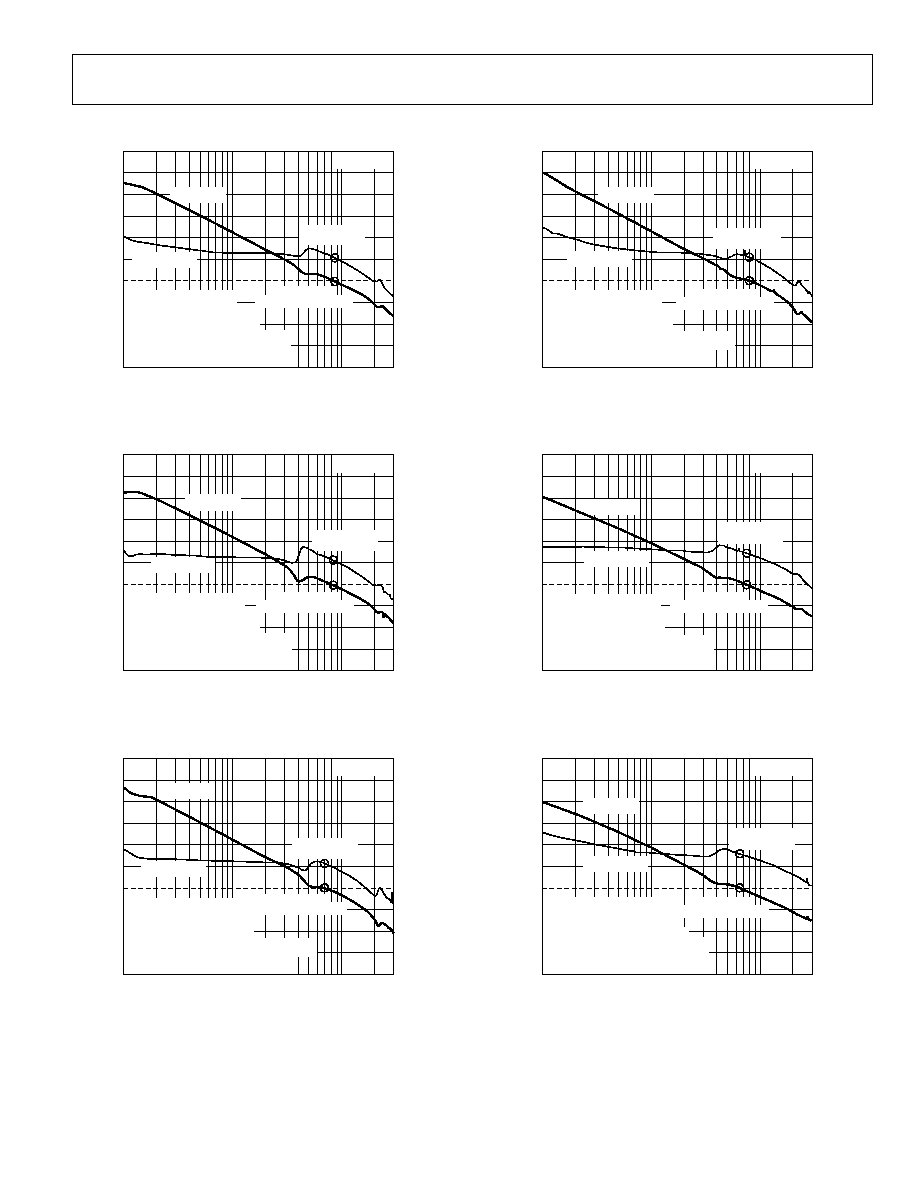
BODE PLOTS
60
≠40
1
300
(kHz)
L
OOP
GA
IN
(
d
B
)
10
100
50
40
30
20
10
0
≠10
≠20
≠30
L
O
O
P
P
H
A
S
E
(
D
eg
rees)
0
45
90
135
180
06
07
9-
05
5
LOOP GAIN
LOOP PHASE
PHASE
MARGIN = 48∞
CROSSOVER
FREQUENCY = 87kHz
ADP2106
OUTPUT VOLTAGE = 1.8V
INPUT VOLTAGE = 5.5V
LOAD CURRENT = 1A
INDUCTOR = 2.2µH (LPS4012)
OUTPUT CAPACITOR = 22µF + 22µF
COMPENSATION RESISTOR = 180k
COMPENSATION CAPACITOR = 56pF
NOTES
1. EXTERNAL COMPONENTS WERE CHOSEN FOR A
5% OVERSHOOT FOR A 1A LOAD TRANSIENT.
Figure 39. ADP2106 Bode Plot at V
IN
= 5.5 V, V
OUT
= 1.8 V and Load = 1 A
60
≠40
1
300
(kHz)
L
OOP
GA
IN
(
d
B
)
10
100
50
40
30
20
10
0
≠10
≠20
≠30
L
O
O
P
P
HAS
E
(
D
eg
r
ees)
0
45
90
135
180
06
07
9-
05
6
NOTES
1. EXTERNAL COMPONENTS WERE CHOSEN FOR A
5% OVERSHOOT FOR A 1A LOAD TRANSIENT.
ADP2106
PHASE
MARGIN = 52∞
LOOP GAIN
LOOP PHASE
OUTPUT VOLTAGE = 1.8V
INPUT VOLTAGE = 3.6V
LOAD CURRENT = 1A
INDUCTOR = 2.2µH (LPS4012)
OUTPUT CAPACITOR = 22µF + 22µF
COMPENSATION RESISTOR = 180k
COMPENSATION CAPACITOR = 56pF
CROSSOVER
FREQUENCY = 83kHz
Figure 40. ADP2106 Bode Plot at V
IN
= 3.6 V, V
OUT
= 1.8 V, and Load = 1 A
60
≠40
1
300
(kHz)
L
OOP
GA
IN
(
d
B
)
10
100
50
40
30
20
10
0
≠10
≠20
≠30
L
O
O
P
P
HAS
E
(
D
eg
re
es)
0
45
90
135
180
06
07
9-
05
7
ADP2105
NOTES
1. EXTERNAL COMPONENTS WERE CHOSEN FOR A
5% OVERSHOOT FOR A 1A LOAD TRANSIENT.
LOOP GAIN
LOOP PHASE
PHASE
MARGIN = 51∞
CROSSOVER
FREQUENCY = 71kHz
OUTPUT VOLTAGE = 1.2V
INPUT VOLTAGE = 3.6V
LOAD CURRENT = 1A
INDUCTOR = 3.3µH (SD3814)
OUTPUT CAPACITOR = 22µF + 22µF + 4.7µF
COMPENSATION RESISTOR = 267k
COMPENSATION CAPACITOR = 39pF
Figure 41. ADP2105 Bode Plot at V
IN
= 3.6 V, V
OUT
= 1.2 V, and Load = 1 A
60
≠40
1
300
(kHz)
L
OOP
GA
IN
(
d
B
)
10
100
50
40
30
20
10
0
≠10
≠20
≠30
L
O
O
P
P
H
AS
E
(
D
eg
r
ees)
0
45
90
135
180
06
07
9-
0
58
ADP2105
NOTES
1. EXTERNAL COMPONENTS WERE CHOSEN FOR A
5% OVERSHOOT FOR A 1A LOAD TRANSIENT.
CROSSOVER
FREQUENCY = 79kHz
PHASE
MARGIN = 49∞
LOOP GAIN
LOOP PHASE
OUTPUT VOLTAGE = 1.2V
INPUT VOLTAGE = 5.5V
LOAD CURRENT = 1A
INDUCTOR = 3.3µH (SD3814)
OUTPUT CAPACITOR = 22µF + 22µF + 4.7µF
COMPENSATION RESISTOR = 267k
COMPENSATION CAPACITOR = 39pF
Figure 42. ADP2105 Bode Plot at V
IN
= 5.5 V, V
OUT
= 1.2 V and Load = 1 A
60
≠40
1
300
(kHz)
L
OOP
GA
IN
(
d
B
)
10
100
50
40
30
20
10
0
≠10
≠20
≠30
L
O
O
P
P
H
A
S
E
(
D
eg
rees)
0
45
90
135
180
0
607
9-
0
59
ADP2107
NOTES
1. EXTERNAL COMPONENTS WERE CHOSEN FOR A
10% OVERSHOOT FOR A 1A LOAD TRANSIENT.
PHASE
MARGIN = 65∞
CROSSOVER
FREQUENCY = 76kHz
OUTPUT VOLTAGE = 2.5V
INPUT VOLTAGE = 5V
LOAD CURRENT = 1A
INDUCTOR = 2µH (D62LCB)
OUTPUT CAPACITOR = 10µF + 4.7µF
COMPENSATION RESISTOR = 70k
COMPENSATION CAPACITOR = 120pF
LOOP PHASE
LOOP GAIN
Figure 43. ADP2107 Bode Plot at V
IN
= 5 V, V
OUT
= 2.5 V and Load = 1 A
60
≠40
1
300
(kHz)
L
OOP
GA
IN
(
d
B
)
10
100
50
40
30
20
10
0
≠10
≠20
≠30
L
O
O
P
P
HAS
E
(
D
e
g
r
ees)
0
45
90
135
180
06
07
9-
06
9
ADP2107
NOTES
1. EXTERNAL COMPONENTS WERE CHOSEN FOR A
10% OVERSHOOT FOR A 1A LOAD TRANSIENT.
LOOP GAIN
LOOP PHASE
PHASE
MARGIN = 70∞
OUTPUT VOLTAGE = 3.3V
INPUT VOLTAGE = 5V
LOAD CURRENT = 1A
INDUCTOR = 2.5µH (CDRH5D28)
OUTPUT CAPACITOR = 10µF + 4.7µF
COMPENSATION RESISTOR = 70k
COMPENSATION CAPACITOR = 120pF
CROSSOVER
FREQUENCY = 67kHz
Figure 44. ADP2107 Bode Plot at V
IN
= 5 V, V
OUT
= 3.3 V, and Load = 1 A

ADP2105/ADP2106/ADP2107
Rev. 0 | Page 20 of 32
LOAD TRANSIENT RESPONSE
06
07
9-
07
5
CH2
50mV~
CH3 1A
CH1 2V
M 10µs
A CH3
0.5A
1
3
2
LX NODE (SWITCH NODE)
OUTPUT VOLTAGE (AC-COUPLED)
OUTPUT CURRENT
OUTPUT CAPACITOR: 22µF + 22µF + 4.7µF
INDUCTOR: SD14, 2.5µH
COMPENSATION RESISTOR: 270k
COMPENSATION CAPACITOR: 39pF
CH2 LOW
≠51mV
Figure 45. 1 A Load Transient Response for ADP2105-1.2
with External Components Chosen for 5% Overshoot
06
079
-
07
7
CH2
100mV~
CH3 1A
CH1 2V
M 10µs
A CH3
0.5A
1
3
2
LX NODE (SWITCH NODE)
OUTPUT VOLTAGE (AC-COUPLED)
OUTPUT CURRENT
OUTPUT CAPACITOR: 22µF + 22µF
INDUCTOR: SD3814, 3.3µH
COMPENSATION RESISTOR: 270k
COMPENSATION CAPACITOR: 39pF
CH2 LOW
≠112mV
Figure 46. 1 A Load Transient Response for ADP2105-1.8
with External Components Chosen for 5% Overshoot
06079-
07
9
CH2
100mV~
CH3 1A
CH1 2V
M 10µs
A CH3
0.5A
1
3
2
LX NODE (SWITCH NODE)
OUTPUT VOLTAGE (AC-COUPLED)
OUTPUT CURRENT
OUTPUT CAPACITOR: 22µF + 4.7µF
INDUCTOR: CDRH5D18, 4.1µH
COMPENSATION RESISTOR: 270k
COMPENSATION CAPACITOR: 39pF
CH2 LOW
≠178mV
Figure 47. 1 A Load Transient Response for ADP2105-3.3
with External Components Chosen for 5% Overshoot
06
079
-
07
6
CH2
50mV~
CH3 1A
CH1 2V
M 10µs
A CH3
0.5A
1
3
2
LX NODE (SWITCH NODE)
OUTPUT VOLTAGE (AC-COUPLED)
OUTPUT CURRENT
OUTPUT CAPACITOR: 22µF + 4.7µF
INDUCTOR: SD14, 2.5µH
COMPENSATION RESISTOR: 135k
COMPENSATION CAPACITOR: 82pF
CH2 LOW
≠93mV
Figure 48. 1 A Load Transient Response for ADP2105-1.2
with External Components Chosen for 10% Overshoot
0
60
79-
07
8
CH2
100mV~
CH3 1A
CH1 2V
M 10µs
A CH3
0.5A
1
3
2
LX NODE (SWITCH NODE)
OUTPUT VOLTAGE (AC-COUPLED)
OUTPUT CURRENT
OUTPUT CAPACITOR: 10µF + 10µF
INDUCTOR: SD3814, 3.3µH
COMPENSATION RESISTOR: 135k
COMPENSATION CAPACITOR: 82pF
CH2 LOW
≠164mV
Figure 49. 1 A Load Transient Response for ADP2105-1.8
with External Components Chosen for 10% Overshoot
06
07
9-
08
0
CH2
200mV~
CH3 1A
CH1 2V
M 10µs
A CH3 0.5A
1
3
2
LX NODE (SWITCH NODE)
OUTPUT VOLTAGE (AC-COUPLED)
OUTPUT CURRENT
OUTPUT CAPACITOR: 10µF + 4.7µF
INDUCTOR: CDRH5D18, 4.1µH
COMPENSATION RESISTOR: 135k
COMPENSATION CAPACITOR: 82pF
CH2 LOW
≠308mV
Figure 50. 1 A Load Transient Response for ADP2105-3.3
with External Components Chosen for 10% Overshoot

ADP2105/ADP2106/ADP2107
Rev. 0 | Page 21 of 32
EFFICIENCY CONSIDERATIONS
Efficiency is defined as the ratio of output power to input power.
The high efficiency of the ADP2105/ADP2106/ADP2107 has
two distinct advantages. First, only a small amount of power is
lost in the dc-to-dc converter package that reduces thermal
constraints. In addition, high efficiency delivers the maximum
output power for the given input power, extending battery life
in portable applications.
There are four major sources of power loss in dc-to-dc
converters like the ADP2105/ADP2106/ADP2107.
∑
Power switch conduction losses
∑
Inductor losses
∑
Switching losses
∑
Transition losses
Power Switch Conduction Losses
Power switch conduction losses are caused by the flow of output
current through the P-channel power switch and the N-channel
synchronous rectifier, which have internal resistances (R
DS(ON)
)
associated with them. The amount of power loss can be approxi-
mated by
P
SW - COND
= [R
DS(ON) - P
◊ D + R
DS(ON) - N
◊ (1 - D)] ◊ I
OUT
2
where D = V
OUT
/V
IN
.
The internal resistance of the power switches increases with
temperature but decreases with higher input voltage. Figure 19
in the Typical Performance Characteristics section shows the
change in R
DS(ON)
vs. input voltage, while Figure 27 in the
Typical Performance Characteristics section shows the change
in R
DS(ON)
vs. temperature for both power devices.
Inductor Losses
Inductor conduction losses are caused by the flow of current
through the inductor, which has an internal resistance (DCR)
associated with it. Larger sized inductors have smaller DCR,
which can improve inductor conduction losses.
Inductor core losses are related to the magnetic permeability of
the core material. Because the ADP2105/ADP2106/ADP2107
are high switching frequency dc-to-dc converters, shielded ferrite
core material is recommended for its low core losses and low EMI.
The total amount of inductor power loss can be calculated by
P
L
= DCR ◊ I
OUT
2
+ Core Losses
Switching Losses
Switching losses are associated with the current drawn by the
driver to turn on and turn off the power devices at the
switching frequency. Each time a power device gate is turned on
and turned off, the driver transfers a charge Q from the input
supply to the gate and then from the gate to ground.
The amount of power loss can by calculated by
P
SW
= (C
GATE - P
+ C
GATE - N
) ◊ V
IN
2
◊ f
SW
where:
(C
GATE - P
+ C
GATE - N
) ~ 600 pF.
f
SW
= 1.2 MHz, the switching frequency.
Transition Losses
Transition losses occur because the P-channel MOSFET power
switch cannot turn on or turn off instantaneously. At the middle of
a LX node transition, the power switch is providing all the inductor
current, while the source to drain voltage of the power switch is
half the input voltage, resulting in power loss. Transition losses
increase with load current and input voltage and occur twice for
each switching cycle.
The amount of power loss can be calculated by
SW
OUT
IN
TRAN
f
t
t
I
V
P
OFF
ON
◊
+
◊
◊
=
)
(
2
where t
ON
and t
OFF
are the rise time and fall time of the LX node,
which are approximately 3 ns.
THERMAL CONSIDERATIONS
In most applications, the ADP2105/ADP2106/ADP2107 do not
dissipate a lot of heat due to their high efficiency. However, in
applications with high ambient temperature, low supply voltage,
and high duty cycle, the heat dissipated in the package is large
enough that it can cause the junction temperature of the die to
exceed the maximum junction temperature of 125∞C. Once the
junction temperature exceeds 140∞C, the converter goes into
thermal shutdown. It recovers only after the junction temperature
has decreased below 100∞C to prevent any permanent damage.
Therefore, thermal analysis for the chosen application solution
is very important to guarantee reliable performance over all
conditions.
The junction temperature of the die is the sum of the ambient
temperature of the environment and the temperature rise of the
package due to the power dissipation, as shown in the following
equation:
T
J
= T
A
+ T
R
where:
T
J
is the junction temperature.
T
A
is the ambient temperature.
T
R
is the rise in temperature of the package due to power
dissipation in it.

ADP2105/ADP2106/ADP2107
Rev. 0 | Page 22 of 32
The rise in temperature of the package is directly proportional
to the power dissipation in the package. The proportionality
constant for this relationship is defined as the thermal
resistance from the junction of the die to the ambient
temperature, as shown in the following equation:
T
R
=
JA
◊ P
D
where:
T
R
is the rise in temperature of the package.
P
D
is the power dissipation in the package.
JA
is the thermal resistance from the junction of the die to the
ambient temperature of the package.
For example, consider an application where the ADP2107-1.8
is used with an input voltage of 3.6 V and a load current of 2 A.
Also, assume that the maximum ambient temperature is 85∞C.
At a load current of 2 A, the most significant contributor of
power dissipation in the dc-to-dc converter package is the
conduction loss of the power switches. Using the graph of
switch resistance vs. temperature (see Figure 27), as well as the
equation of power loss given in the Power Switch Conduction
Losses section, the power dissipation in the package can be
calculated by
P
SW - COND
= [R
DS(ON) - P
◊ D + R
DS(ON) - N
◊ (1 - D)] ◊ I
OUT
2
=
[109 m ◊ 0.5 + 90 m ◊ 0.5] ◊ (2 A)
2
~ 400 mW
The
JA
for the LFCSP_VQ package is 40∞C/W, as shown in
Table 3. Thus, the rise in temperature of the package due to
power dissipation is
T
R
=
JA
◊ P
D
= 40∞C/W ◊ 0.40 W = 16∞C
The junction temperature of the converter is
T
J
= T
A
+ T
R
= 85∞C + 16∞C = 101∞C
which is below the maximum junction temperature of 125∞C.
Thus, this application operates reliably from a thermal point
of view.
DESIGN EXAMPLE
Consider an application with the following specifications:
Input Voltage = 3.6 V to 4.2 V.
Output Voltage = 2 V.
Typical Output Current = 600 mA.
Maximum Output Current = 1.2 A.
Soft Start Time = 2 ms.
Overshoot 100 mV under all load transient conditions.
1.
Choose the dc-to-dc converter that satisfies the maximum
output current requirement. Because the maximum output
current for this application is 1.2 A, the ADP2106 with a
maximum output current of 1.5 A is ideal for this
application.
2.
See whether the output voltage desired is available as a
fixed output voltage option. Because 2 V is not one of the
fixed output voltage options available, choose the adjustable
version of ADP2106.
3.
The first step in external component selection for an
adjustable version converter is to calculate the resistance of
the resistive voltage divider that sets the output voltage.
=
=
=
k
40
20
V
8
.
0
A
I
V
R
STRING
FB
BOT
=
-
◊
=
-
=
k
60
V
8
.
0
V
8
.
0
V
2
k
40
FB
FB
OUT
BOT
TOP
V
V
V
R
R
4.
Calculate the minimum inductor value as follows:
For the ADP2106:
L > (0.83 H/V) ◊ V
OUT
L > 0.83 H/V ◊ 2 V
L > 1.66 H
Next, calculate the ideal inductor value that sets the
inductor peak-to-peak current ripple, I
L
, to1/3 of the
maximum load current at the maximum input voltage.
=
◊
-
◊
◊
=
H
)
(
5
.
2
)
(MAX
LOAD
IN
OUT
IN
OUT
IDEAL
I
V
V
V
V
L
H
2.18
H
2
.
1
2
.
4
)
2
2
.
4
(
2
5
.
2
=
◊
-
◊
◊
The closest standard inductor value is 2.2 H. The
maximum rms current of the inductor should be greater
than 1.2 A, and the saturation current of the inductor
should be greater than 2 A. One inductor that meets these
criteria is the LPS4012-2.2 H from Coilcraft.
5.
Choose the output capacitor based on the transient
response requirements. The worst-case load transient is
1.2 A, for which the overshoot must be less than 100 mV,
which is 5% of the output voltage. Therefore, for a 1 A load
transient, the overshoot must be less than 4% of the output
voltage. For these conditions, Figure 37 gives
Output Capacitor ◊ Output Voltage = 60 C
F
30
V
0
.
2
C
60
=
Capacitor
Output
Next, taking into account the loss of capacitance due to dc
bias, as shown in Figure 38, two 22 F X5R MLCC capacitors
from Murata (GRM21BR60J226M) are sufficient for this
application.

ADP2105/ADP2106/ADP2107
Rev. 0 | Page 23 of 32
6.
Because the ADP2106 is being used in this application, the
input capacitors are 10 F and 4.7 F X5R Murata capacitors
(GRM21BR61A106K and GRM21BR61A475K).
7.
The input filter consists of a small 0.1 F ceramic capacitor
placed between IN and AGND and a 10 resistor placed
between IN and PWIN1.
8.
Choose a soft start capacitor of 2 nF to achieve a soft start
time of 2 ms.
9.
Finally, the compensation resistor and capacitor can be
calculated as
=
REF
OUT
OUT
CS
m
CROSS
COMP
V
V
C
G
G
F
R
)
2
(
8
.
0
=
◊
◊
◊
=
k
215
V
8
.
0
V
2
F
30
V
/
A
8125
.
2
V
/
A
50
kHz
80
)
2
(
8
.
0
pF
39
k
215
kHz
80
2
2
=
◊
◊
=
=
COMP
CROSS
COMP
R
F
C

ADP2105/ADP2106/ADP2107
Rev. 0 | Page 24 of 32
EXTERNAL COMPONENT RECOMMENDATIONS
Table 10. Recommended External Components for Popular Output Voltage Options at 80 kHz Crossover Frequency with
10% Overshoot for a 1 A Load Transient (Refer to Figure 35 and Figure 36)
Part V
OUT
(V)
C
IN1
1
(F)
C
IN2
2
(F)
C
OUT
3
(F)
L (H)
R
COMP
(k)
C
COMP
(pF)
R
TOP
4
(k)
R
BOT
5
(k)
ADP2105-ADJ
0.9
4.7
4.7
22 + 10
2.0
135
82
5
40
ADP2105-ADJ
1.2
4.7
4.7
22 + 4.7
2.5
135
82
20
40
ADP2105-ADJ
1.5
4.7
4.7
10 + 10
3.0
135
82
35
40
ADP2105-ADJ
1.8
4.7
4.7
10 + 10
3.3
135
82
50
40
ADP2105-ADJ
2.5
4.7
4.7
10 + 4.7
3.6
135
82
85
40
ADP2105-ADJ
3.3
4.7
4.7
10 + 4.7
4.1
135
82
125
40
ADP2106-ADJ
0.9
4.7
10
22 + 10
1.5
90
100
5
40
ADP2106-ADJ
1.2
4.7
10
22 + 4.7
1.8
90
100
20
40
ADP2106-ADJ
1.5
4.7
10
10 + 10
2.0
90
100
35
40
ADP2106-ADJ
1.8
4.7
10
10 + 10
2.2
90
100
50
40
ADP2106-ADJ
2.5
4.7
10
10 + 4.7
2.5
90
100
85
40
ADP2106-ADJ
3.3
4.7
10
10 + 4.7
3.0
90
100
125
40
ADP2107-ADJ
0.9
10
10
22 + 10
1.2
70
120
5
40
ADP2107-ADJ
1.2
10
10
22 + 4.7
1.5
70
120
20
40
ADP2107-ADJ
1.5
10
10
10 + 10
1.5
70
120
35
40
ADP2107-ADJ
1.8
10
10
10 + 10
1.8
70
120
50
40
ADP2107-ADJ
2.5
10
10
10 + 4.7
1.8
70
120
85
40
ADP2107-ADJ
3.3
10
10
10 + 4.7
2.5
70
120
125
40
ADP2105-1.2
1.2
4.7
4.7
22 + 4.7
2.5
135
82
-
-
ADP2105-1.5
1.5
4.7
4.7
10 + 10
3.0
135
82
-
-
ADP2105-1.8
1.8
4.7
4.7
10 + 10
3.3
135
82
-
-
ADP2105-3.3
3.3
4.7
4.7
10 + 4.7
4.1
135
82
-
-
ADP2106-1.2
1.2
4.7
10
22 + 4.7
1.8
90
100
-
-
ADP2106-1.5
1.5
4.7
10
10 + 10
2.0
90
100
-
-
ADP2106-1.8
1.8
4.7
10
10 + 10
2.2
90
100
-
-
ADP2106-3.3
3.3
4.7
10
10 + 4.7
3.0
90
100
-
-
ADP2107-1.2
1.2
10
10
22 + 4.7
1.5
70
120
-
-
ADP2107-1.5
1.5
10
10
10 + 10
1.5
70
120
-
-
ADP2107-1.8
1.8
10
10
10 + 10
1.8
70
120
-
-
ADP2107-3.3
3.3
10
10
10 + 4.7
2.5
70
120
-
-
1
4.7 F 0805 X5R 10 V Murata≠GRM21BR61A475KA73L.
10 F 0805 X5R 10 V Murata≠GRM21BR61A106KE19L.
2
4.7 F 0805 X5R 10 V Murata≠GRM21BR61A475KA73L.
10 F 0805 X5R 10 V Murata≠GRM21BR61A106KE19L.
3
4.7 F 0805 X5R 10 V Murata≠GRM21BR61A475KA73L.
10 F 0805 X5R 10 V Murata≠GRM21BR61A106KE19L.
22 F 0805 X5R 6.3 V Murata≠GRM21BR60J226ME39L.
4
0.5% accuracy resistor.
5
0.5% accuracy resistor.

ADP2105/ADP2106/ADP2107
Rev. 0 | Page 25 of 32
Table 11. Recommended External Components for Popular Output Voltage Options at 80 kHz Crossover Frequency with
5% Overshoot for a 1 A Load Transient (Refer to Figure 35 and Figure 36)
Part V
OUT
(V) C
IN1
1
(F)
C
IN2
2
(F)
C
OUT
3
(F)
L (H)
R
COMP
(k)
C
COMP
(pF)
R
TOP
4
(k)
R
BOT
5
(k)
ADP2105-ADJ
0.9
4.7
4.7
22 + 22 + 22
2.0
270
39
5
40
ADP2105-ADJ
1.2
4.7
4.7
22 + 22 + 4.7
2.5
270
39
20
40
ADP2105-ADJ
1.5
4.7
4.7
22 + 22
3.0
270
39
35
40
ADP2105-ADJ
1.8
4.7
4.7
22 + 22
3.3
270
39
50
40
ADP2105-ADJ
2.5
4.7
4.7
22 + 10
3.6
270
39
85
40
ADP2105-ADJ
3.3
4.7
4.7
22 + 4.7
4.1
270
39
125
40
ADP2106-ADJ
0.9
4.7
10
22 + 22 + 22
1.5
180
56
5
40
ADP2106-ADJ
1.2
4.7
10
22 + 22 + 4.7
1.8
180
56
20
40
ADP2106-ADJ
1.5
4.7
10
22 + 22
2.0
180
56
35
40
ADP2106-ADJ
1.8
4.7
10
22 + 22
2.2
180
56
50
40
ADP2106-ADJ
2.5
4.7
10
22 + 10
2.5
180
56
85
40
ADP2106-ADJ
3.3
4.7
10
22 + 4.7
3.0
180
56
125
40
ADP2107-ADJ
0.9
10
10
22 + 22 + 22
1.2
140
68
5
40
ADP2107-ADJ
1.2
10
10
22 + 22 + 4.7
1.5
140
68
20
40
ADP2107-ADJ
1.5
10
10
22 + 22
1.5
140
68
35
40
ADP2107-ADJ
1.8
10
10
22 + 22
1.8
140
68
50
40
ADP2107-ADJ
2.5
10
10
22 + 10
1.8
140
68
85
40
ADP2107-ADJ
3.3
10
10
22 + 4.7
2.5
140
68
125
40
ADP2105-1.2
1.2
4.7
4.7
22 + 22 + 4.7
2.5
270
39
-
-
ADP2105-1.5
1.5
4.7
4.7
22 + 22
3.0
270
39
-
-
ADP2105-1.8
1.8
4.7
4.7
22 + 22
3.3
270
39
-
-
ADP2105-3.3
3.3
4.7
4.7
22 + 4.7
4.1
270
39
-
-
ADP2106-1.2
1.2
4.7
10
22 + 22 + 4.7
1.8
180
56
-
-
ADP2106-1.5
1.5
4.7
10
22 + 22
2.0
180
56
-
-
ADP2106-1.8
1.8
4.7
10
22 + 22
2.2
180
56
-
-
ADP2106-3.3
3.3
4.7
10
22 + 4.7
3.0
180
56
-
-
ADP2107-1.2
1.2
10
10
22 + 22 + 4.7
1.5
140
68
-
-
ADP2107-1.5
1.5
10
10
22 + 22
1.5
140
68
-
-
ADP2107-1.8
1.8
10
10
22 + 22
1.8
140
68
-
-
ADP2107-3.3
3.3
10
10
22 + 4.7
2.5
140
68
-
-
1
4.7F 0805 X5R 10V Murata ≠ GRM21BR61A475KA73L
10F 0805 X5R 10V Murata ≠ GRM21BR61A106KE19L
2
4.7F 0805 X5R 10V Murata ≠ GRM21BR61A475KA73L
10F 0805 X5R 10V Murata ≠ GRM21BR61A106KE19L
3
4.7F 0805 X5R 10V Murata ≠ GRM21BR61A475KA73L
10F 0805 X5R 10V Murata ≠ GRM21BR61A106KE19L
22F 0805 X5R 6.3V Murata ≠ GRM21BR60J226ME39L
4
0.5% Accuracy Resistor
5
0.5% Accuracy Resistor

ADP2105/ADP2106/ADP2107
Rev. 0 | Page 26 of 32
CIRCUIT BOARD LAYOUT RECOMMENDATIONS
Good circuit board layout is essential in obtaining the best
performance from the ADP2105/ADP2106/ADP2107. Poor
circuit layout degrades the output ripple, as well as the
electromagnetic interference (EMI) and electromagnetic
compatibility (EMC) performance.
Figure 52 and Figure 53 show the ideal circuit board layout for
the ADP2105/ADP2106/ADP2107. Use this layout to achieve
the highest performance. Refer to the following guidelines if
adjustments to the suggested layout are needed.
∑
Use separate analog and power ground planes. Connect
the ground reference of sensitive analog circuitry (such as
compensation and output voltage divider components) to
analog ground; connect the ground reference of power
components (such as input and output capacitors) to power
ground. In addition, connect both the ground planes to the
exposed pad of the ADP2105/ADP2106/ADP2107.
∑
For each PWIN pin, place an input capacitor as close to the
PWIN pin as possible and connect the other end to the closest
power ground plane.
∑
Place the 0.1 F, 10 low-pass input filter between the IN
pin and the PWIN1 pin, as close to the IN pin as possible.
∑
Ensure that the high current loops are as short and as wide
as possible. Make the high current path from C
IN
through
L, C
OUT
, and the PGND plane back to C
IN
as short as possible.
To accomplish this, ensure that the input and output
capacitors share a common PGND plane.
Also, make the high current path from PGND pin of the
ADP2105/ADP2106/ADP2107 through L and C
OUT
back
to the PGND plane as short as possible. To do this, ensure
that the PGND pin of the ADP2105/ADP2106/ADP2107
is tied to the PGND plane as close as possible to the input
and output capacitors.
∑
Place the feedback resistor divider network as close as
possible to the FB pin to prevent noise pickup. Try to
minimize the length of trace connecting the top of the
feedback resistor divider to the output while keeping away
from the high current traces and the switch node (LX) that
can lead to noise pickup. To reduce noise pickup, place an
analog ground plane on either side of the FB trace. For the
low fixed voltage options (1.2 V and 1.5 V), poor routing
of the OUT_SENSE trace can lead to noise pickup, adversely
affecting load regulation. This can be fixed by placing a 1 nF
bypass capacitor close to the OUT_SENSE pin.
∑
The placement and routing of the compensation components
are critical for proper behavior of the ADP2105/ADP2106/
ADP2107. The compensation components should be placed
as close to the COMP pin as possible. It is advisable to use
0402-sized compensation components for closer placement,
leading to smaller parasitics. Surround the compensation
components with analog ground plane to prevent noise
pickup. Also, ensure that the metal layer under the
compensation components is the analog ground plane.
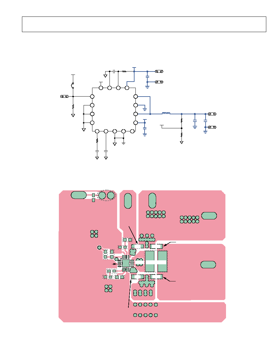
ADP2105/ADP2106/ADP2107
Rev. 0 | Page 27 of 32
EVALUATION BOARD
EVALUATION BOARD SCHEMATIC (ADP2107-1.8)
J1
U1
EN
VCC
INPUT VOLTAGE = 2.7V TO 5.5V
OUTPUT VOLTAGE = 1.8V, 2A
V
OUT
VIN
GND
OUT
VCC
OUT
2
1
GND
VCC
ADP2107-1.8
EN
SS
LX2
AGND
COMP
PGND
GND
GND
GND
NC
PADDLE
LX1
PWIN2
1
2
3
4
12
11
10
9
16
15
14
13
5
6
7
8
17
R2
100k
C6
68pF
C5
1nF
R1
140k
C2
10µF
1
L1
2
2µH
C3
22µF
1
C4
22µF
1
R4
0
R5
NS
R3
10
C7
0.1µF
C1
10µF
1
NC = NO CONNECT
06
07
9-
0
44
1
MURATA X5R 0805
10F: GRM21BR61A106KE19L
22F: GRM21BR60J226ME39L
2
2H INDUCTOR D62LCB TOKO
OUT_SENSE
PWIN1
IN
GND
Figure 51. Evaluation Board Schematic of the ADP2107-1.8 (Bold Traces Are High Current Paths)
RECOMMENDED PCB BOARD LAYOUT (EVALUATION BOARD LAYOUT)
GROUND
GROUND
CONNECT THE GROUND RETURN OF
ALL POWER COMPONENTS SUCH AS
INPUT AND OUTPUT CAPACITORS TO
THE POWER GROUND PLANE.
POWER GROUND
PLANE
OUTPUT CAPACITOR
OUTPUT CAPACITOR
C
OUT
INPUT CAPACITOR
INPUT CAPACITOR
OUTPUT
V
OUT
C
IN
C
OUT
C
IN
JUMPER TO ENABLE
ENABLE
100k PULL-DOWN
V
IN
INPUT
PLACE THE FEEDBACK RESISTORS AS
CLOSE TO THE FB PIN AS POSSIBLE.
ADP2105/ADP2106/ADP2107
R
TOP
R
BOT
C
SS
R
COMP
C
COMP
PLACE THE COMPENSATION
COMPONENTS AS CLOSE TO
THE COMP PIN AS POSSIBLE.
ANALOG GROUND PLANE
CONNECT THE GROUND RETURN OF ALL
SENSITIVE ANALOG CIRCUITRY SUCH AS
COMPENSATION AND OUTPUT VOLTAGE
DIVIDER TO THE ANALOG GROUND PLANE.
LX
LX
PGND
INDUCTOR (L)
POWER GROUND
0
60
79
-
04
5
Figure 52. Recommended Layout of Top Layer of ADP2105/ADP2106/ADP2107
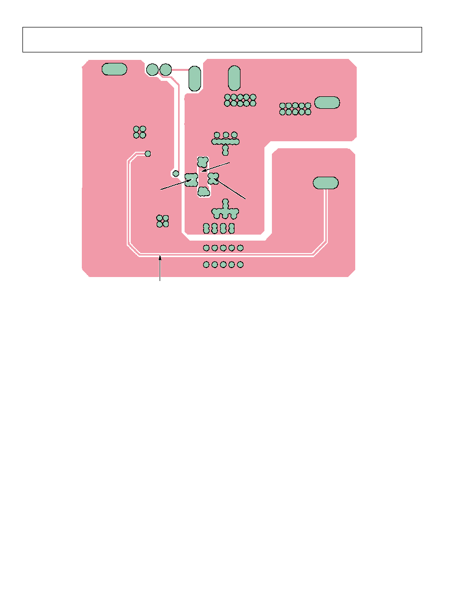
ADP2105/ADP2106/ADP2107
Rev. 0 | Page 28 of 32
POWER GROUND PLANE
INPUT VOLTAGE PLANE
CONNECTING THE TWO
PWIN PINS AS CLOSE
AS POSSIBLE.
CONNECT THE PGND PIN
TO THE POWER GROUND
PLANE AS CLOSE TO THE
ADP2105/ADP2106/ADP2107
AS POSSIBLE.
CONNECT THE EXPOSED PAD OF
THE ADP2105/ADP2106/ADP2107
TO A LARGE GROUND PLANE TO
AID POWER DISSIPATION.
FEEDBACK TRACE: THIS TRACE CONNECTS THE TOP OF THE
RESISTIVE VOLTAGE DIVIDER ON THE FB PIN TO THE OUTPUT.
PLACE THIS TRACE AS FAR AWAY FROM THE LX NODE AND HIGH
CURRENT TRACES AS POSSIBLE TO PREVENT NOISE PICKUP.
V
IN
V
IN
ANALOG GROUND PLANE
ENABLE
GND
GND
06
07
9-
0
46
V
OUT
Figure 53. Recommended Layout of Bottom Layer of ADP2105/ADP2106/ADP2107
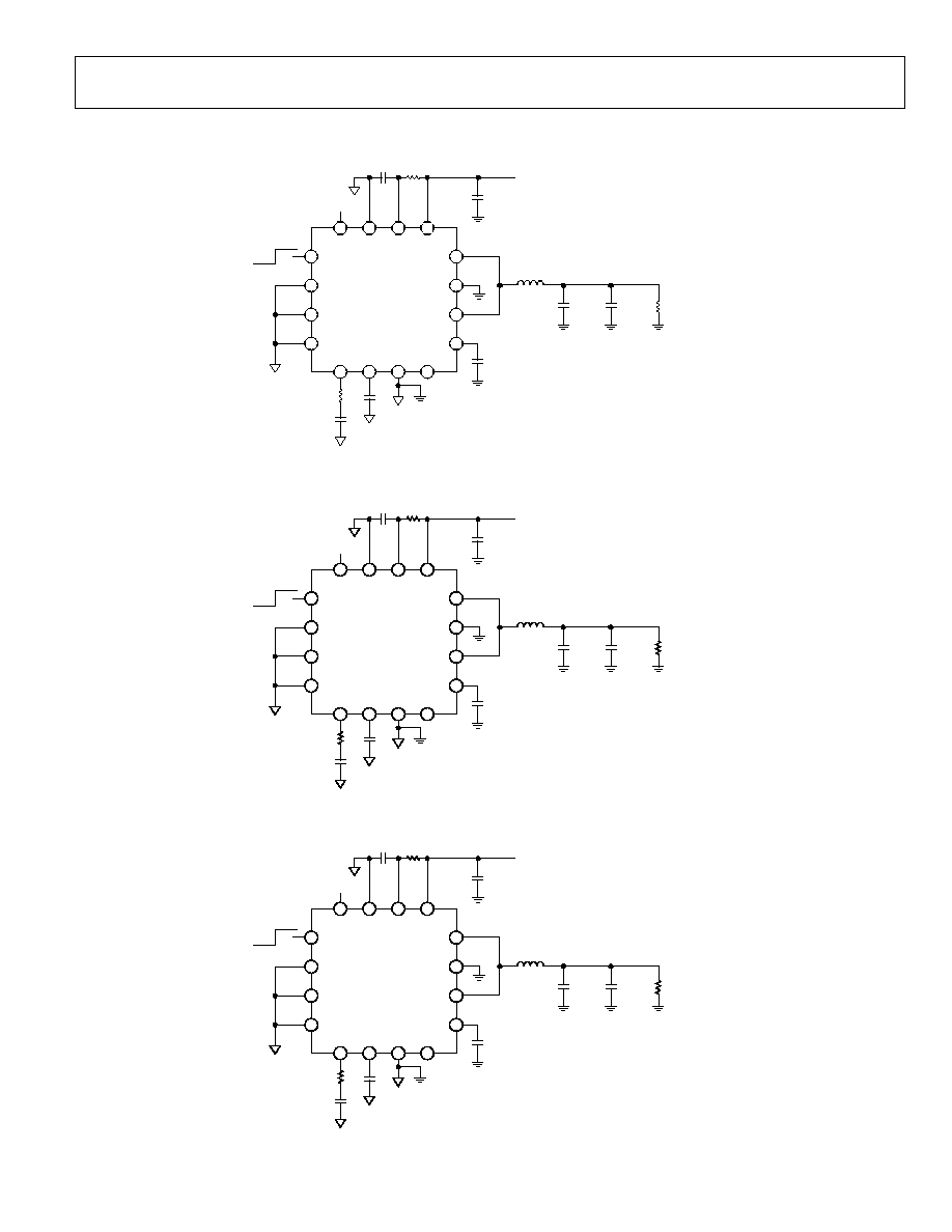
ADP2105/ADP2106/ADP2107
Rev. 0 | Page 29 of 32
APPLICATION CIRCUITS
ADP2107-3.3
OFF
EN
SS
LX2
AGND
OUTPUT VOLTAGE = 3.3V
COMP
ON
PGND
GND
GND
GND
NC
LX1
PWIN2
V
IN
V
IN
INPUT VOLTAGE = 5V
10F
1
V
OUT
V
OUT
1nF
70k
120pF
1
2
3
4
12
11
10
9
16
15
14
13
5
6
7
8
2.5H
2
4.7F
1
LOAD
0A TO 2A
10F
1
10F
1
10
0.1F
1
MURATA X5R 0805
10F: GRM21BR61A106KE19L
4.7F: GRM21BR61A475KA73L
2
SUMIDA CDRH5D28: 2.5H
NOTES
1. NC = NO CONNECT.
2. EXTERNAL COMPONENTS WERE
CHOSEN FOR A 10% OVERSHOOT
FOR A 1A LOAD TRANSIENT.
060
79
-
0
47
OUT_SENSE
PWIN1
IN
GND
Figure 54. Application Circuit--V
IN
= 5 V, V
OUT
= 3.3 V, LOAD = 0 A to 2 A
ADP2107-1.5
OFF
EN
SS
LX2
AGND
OUTPUT VOLTAGE = 1.5V
COMP
ON
PGND
GND
GND
GND
NC
LX1
PWIN2
V
IN
V
IN
INPUT VOLTAGE = 3.6V
22F
1
V
OUT
V
OUT
1nF
140k
68pF
1
2
3
4
12
11
10
9
16
15
14
13
5
6
7
8
1.5H
2
22F
1
LOAD
0A TO 2A
10F
1
10F
1
10
0.1F
1
MURATA X5R 0805
10F: GRM21BR61A106KE19L
22F: GRM21BR60J226ME39L
2
TOKO D62LCB OR COILCRAFT LPS4012
NOTES
1. NC = NO CONNECT.
2. EXTERNAL COMPONENTS WERE
CHOSEN FOR A 5% OVERSHOOT
FOR A 1A LOAD TRANSIENT.
0607
9-
0
48
OUT_SENSE
PWIN1
IN
GND
Figure 55. Application Circuit--V
IN
= 3.6 V, V
OUT
= 1.5 V, LOAD = 0 A to 2 A
ADP2105-1.8
OFF
EN
SS
LX2
AGND
OUTPUT VOLTAGE = 1.8V
COMP
ON
PGND
GND
GND
GND
NC
LX1
PWIN2
V
IN
V
IN
INPUT VOLTAGE = 2.7V TO 4.2V
22F
1
V
OUT
V
OUT
1nF
270k
39pF
1
2
3
4
12
11
10
9
16
15
14
13
5
6
7
8
2.7H
2
22F
1
LOAD
0A TO 1A
4.7F
1
4.7F
1
10
0.1F
1
MURATA X5R 0805
4.7F: GRM21BR61A475KA73L
22F: GRM21BR60J226ME39L
2
TOKO 1098AS-DE2812: 2.7H
NOTES
1. NC = NO CONNECT.
2. EXTERNAL COMPONENTS WERE
CHOSEN FOR A 5% OVERSHOOT
FOR A 1A LOAD TRANSIENT.
0
6079
-
04
9
OUT_SENSE
PWIN1
IN
GND
Figure 56. Application Circuit--V
IN
= Li-Ion Battery, V
OUT
= 1.8 V, LOAD = 0 A to 1 A

ADP2105/ADP2106/ADP2107
Rev. 0 | Page 30 of 32
ADP2105-1.2
OFF
EN
SS
LX2
AGND
OUTPUT VOLTAGE = 1.2V
COMP
ON
PGND
GND
GND
GND
NC
LX1
PWIN2
V
IN
V
IN
INPUT VOLTAGE = 2.7V TO 4.2V
22F
1
V
OUT
V
OUT
1nF
135k
82pF
1
2
3
4
12
11
10
9
16
15
14
13
5
6
7
8
2.4H
2
4.7F
1
LOAD
0A TO 1A
4.7F
1
4.7F
1
10
0.1F
1
MURATA X5R 0805
4.7F: GRM21BR61A475KA73L
22F: GRM21BR60J226ME39L
2
TOKO 1069AS-DB3018HCT OR
TOKO 1070AS-DB3020HCT
NOTES
1. NC = NO CONNECT.
2. EXTERNAL COMPONENTS WERE
CHOSEN FOR A 10% OVERSHOOT
FOR A 1A LOAD TRANSIENT.
06
07
9-
0
50
OUT_SENSE
PWIN1
IN
GND
Figure 57. Application Circuit--V
IN
= Li-Ion Battery, V
OUT
= 1.2 V, LOAD = 0 A to 1 A
ADP2106-ADJ
OFF
EN
SS
LX2
FB
PWIN1
AGND
OUTPUT VOLTAGE = 2.5V
COMP
ON
PGND
IN
GND
GND
GND
NC
GND
LX1
PWIN2
V
IN
V
IN
INPUT VOLTAGE = 5V
FB
1nF
180k
56pF
1
2
3
4
12
11
10
9
16
15
14
13
5
6
7
8
2.5H
2
10F
1
22F
1
LOAD
0A TO 1.5A
4.7F
1
10F
1
10
0.1F
1
MURATA X5R 0805
4.7F: GRM21BR61A475KA73L
10F: GRM21BR61A106KE19L
22F: GRM21BR60J226ME39L
2
COILTRONICS SD14: 2.5H
NOTES
1. NC = NO CONNECT.
2. EXTERNAL COMPONENTS WERE
CHOSEN FOR A 5% OVERSHOOT
FOR A 1A LOAD TRANSIENT.
85k
40k
FB
06
07
9-
05
1
Figure 58. Application Circuit--V
IN
= 5 V, V
OUT
= 2.5 V, LOAD = 0 A to 1.5 A
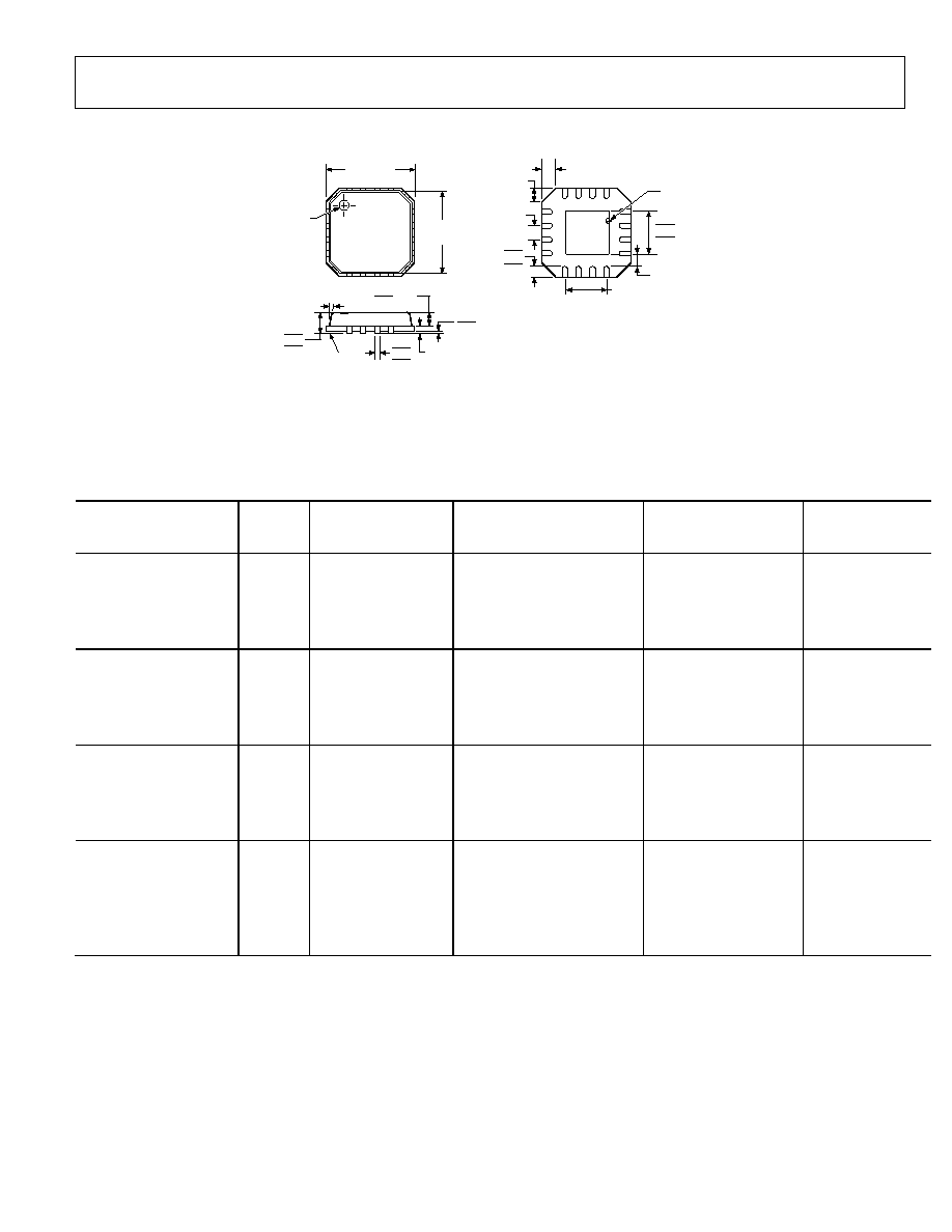
ADP2105/ADP2106/ADP2107
Rev. 0 | Page 31 of 32
OUTLINE DIMENSIONS
COMPLIANT TO JEDEC STANDARDS MO-220-VGGC
2.25
2.10 SQ
1.95
16
5
13
8
9
12
1
4
1.95 BSC
PIN 1
INDICATOR
TOP
VIEW
4.00
BSC SQ
3.75
BSC SQ
COPLANARITY
0.08
EXPOSED
PAD
(BOTTOM VIEW)
12∞ MAX
1.00
0.85
0.80
SEATING
PLANE
0.35
0.30
0.25
0.80 MAX
0.65 TYP
0.05 MAX
0.02 NOM
0.20 REF
0.65 BSC
0.60 MAX
0.60 MAX
PIN 1
INDICATOR
0.25 MIN
01
06
06
-
0
0.75
0.60
0.50
Figure 59. 16-Lead Lead Frame Chip Scale Package [LFCSP_VQ]
4 mm ◊ 4 mm Body, Very Thin Quad
(CP-16-4)
Dimensions shown in millimeters
ORDERING GUIDE
Model
Output
Current
Junction
Temperature
Range
Output Voltage
Package Description
Package Option
ADP2105ACPZ-1.2-R7
1
1 A
-40∞C to +125∞C
1.2 V
16-Lead LFCSP_VQ
CP-16-4
ADP2105ACPZ-1.5-R7
1
1 A
-40∞C to +125∞C
1.5 V
16-Lead LFCSP_VQ
CP-16-4
ADP2105ACPZ-1.8-R7
1
1 A
-40∞C to +125∞C
1.8 V
16-Lead LFCSP_VQ
CP-16-4
ADP2105ACPZ-3.3-R7
1
1 A
-40∞C to +125∞C
3.3 V
16-Lead LFCSP_VQ
CP-16-4
ADP2105ACPZ-R7
1
1 A
-40∞C to +125∞C
ADJ
16-Lead LFCSP_VQ
CP-16-4
ADP2106ACPZ-1.2-R7
1
1.5 A
-40∞C to +125∞C
1.2 V
16-Lead LFCSP_VQ
CP-16-4
ADP2106ACPZ-1.5-R7
1
1.5 A
-40∞C to +125∞C
1.5 V
16-Lead LFCSP_VQ
CP-16-4
ADP2106ACPZ-1.8-R7
1
1.5 A
-40∞C to +125∞C
1.8 V
16-Lead LFCSP_VQ
CP-16-4
ADP2106ACPZ-3.3-R7
1
1.5 A
-40∞C to +125∞C
3.3 V
16-Lead LFCSP_VQ
CP-16-4
ADP2106ACPZ-R7
1
1.5 A
-40∞C to +125∞C
ADJ
16-Lead LFCSP_VQ
CP-16-4
ADP2107ACPZ-1.2-R7
1
2 A
-40∞C to +125∞C
1.2 V
16-Lead LFCSP_VQ
CP-16-4
ADP2107ACPZ-1.5-R7
1
2 A
-40∞C to +125∞C
1.5 V
16-Lead LFCSP_VQ
CP-16-4
ADP2107ACPZ-1.8-R7
1
2 A
-40∞C to +125∞C
1.8 V
16-Lead LFCSP_VQ
CP-16-4
ADP2107ACPZ-3.3-R7
1
2 A
-40∞C to +125∞C
3.3 V
16-Lead LFCSP_VQ
CP-16-4
ADP2107ACPZ-R7
1
2 A
-40∞C to +125∞C
ADJ
16-Lead LFCSP_VQ
CP-16-4
ADP2105-1.8-EVAL
1.8
V
Evaluation
Board
ADP2105-EVAL
Adjustable, but set to 2.5 V
Evaluation Board
ADP2106-1.8-EVAL
1.8
V
Evaluation
Board
ADP2106-EVAL
Adjustable, but set to 2.5 V
Evaluation Board
ADP2107-1.8-EVAL
1.8
V
Evaluation
Board
ADP2107-EVAL
Adjustable, but set to 2.5 V
Evaluation Board
1
Z = Pb-free part.

ADP2105/ADP2106/ADP2107
Rev. 0 | Page 32 of 32
NOTES
©2006 Analog Devices, Inc. All rights reserved. Trademarks and
registered trademarks are the property of their respective owners.
D06079-0-7/06(0)