 | –≠–ª–µ–∫—Ç—Ä–æ–Ω–Ω—ã–π –∫–æ–º–ø–æ–Ω–µ–Ω—Ç: ADP3041 | –°–∫–∞—á–∞—Ç—å:  PDF PDF  ZIP ZIP |
Document Outline
- FEATURES
- GENERAL DESCRIPTION
- FUNCTIONAL BLOCK DIAGRAM
- SPECIFICATIONS
- ABSOLUTE MAXIMUM RATINGS
- ORDERING GUIDE
- PIN CONFIGURATION
- PIN FUNCTION DESCRIPTIONS
- Typical Performance Characteristics
- THEORY OF OPERATION
- Switching Regulator
- Soft Start
- Buffers
- Input Overvoltage Protection
- Output Phase Reversal
- APPLICATION INFORMATION
- Output Voltage
- Inductor Selection
- Capacitor Selection
- Diode Selection
- Loop Compensation
- Shutdown
- Layout Procedure
- OUTLINE DIMENSIONS
- Revision History
REV. D
Information furnished by Analog Devices is believed to be accurate and
reliable. However, no responsibility is assumed by Analog Devices for its
use, nor for any infringements of patents or other rights of third parties that
may result from its use. No license is granted by implication or otherwise
under any patent or patent rights of Analog Devices. Trademarks and
registered trademarks are the property of their respective owners.
One Technology Way, P.O. Box 9106, Norwood, MA 02062-9106, U.S.A.
Tel: 781/329-4700
www.analog.com
Fax: 781/326-8703
© 2003 Analog Devices, Inc. All rights reserved.
ADP3041
TFT LCD Panel Power Module
FEATURES
600 kHz PWM Frequency
Fully Integrated 1.5 A Power Switch
3% Output Regulation Accuracy
Simple Compensation
Small Inductor and MLC Capacitors
300 A Quiescent Supply Current
90% Efficiency
Undervoltage Lockout
5 Buffers
TSSOP 20-Lead Package
Pb-Free Part
APPLICATIONS
TFT LCD Bias Supplies
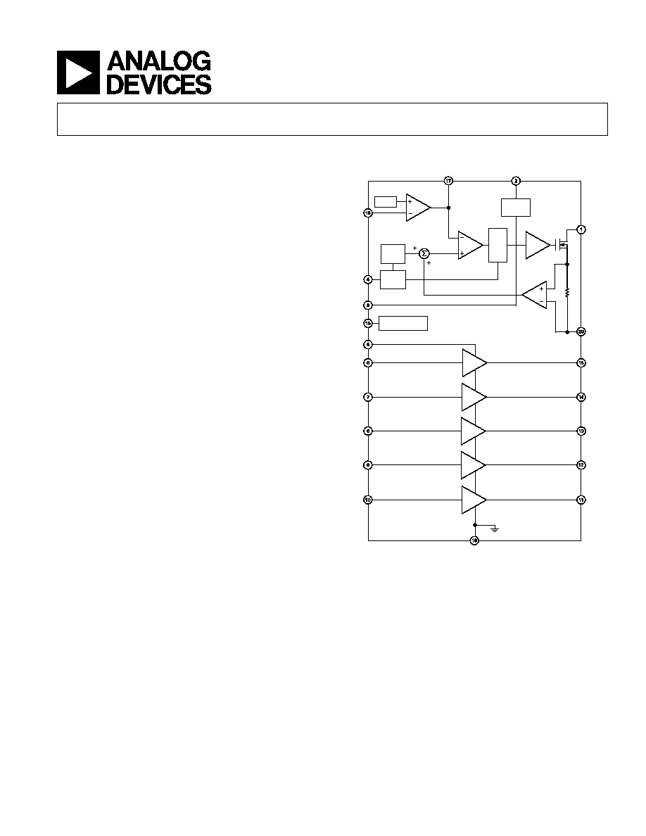
FUNCTIONAL BLOCK DIAGRAM
RAMP
GEN
Q
S
R
F/F
NC
DRIVER
CURRENT
SENSE
AMPLIFIER
COMP
SW
FB
IN
COMPARATOR
ERROR
AMP
PGND
BIAS
gm
SD
OSC
ADP3041
SS
VCMO
G1O
AGND
G2O
G3O
G4O
G1I
G2I
G3I
G4I
VCMI
AVCC
SOFT START
REF
GENERAL DESCRIPTION
The ADP3041 is a fixed frequency, PWM step-up dc-to-dc
switching regulator with five buffers capable of 12 V boosted
output voltage in a TSSOP 20-lead package. It provides high
efficiency, low noise operation, and excellent dynamic response,
and is easy to use. The high switching frequency allows for small,
cost-saving, external inductive and capacitive components. The
ADP3041 operates in PWM current mode. The current limit
and the power switch are integrated completely on-chip.
Capable of operating from 2.5 V to 5.5 V input, the ADP3041
is ideal for thin-film transistor (TFT) liquid crystal display
(LCD) module applications, where local point-of-use power
regulation is required. Supporting output voltages down to 4.5 V,
the ADP3041 is ideal to generate today's low voltage rails, pro-
viding the optimal solution in its class for delivering power
efficiently, responsively, and simply with minimal printed circuit
board area.
The ADP3041 integrates five buffers. Each buffer can deliver
35 mA output current and has rail-to-rail input and output
capability.

REV. D
≠2≠
ADP3041≠SPECIFICATIONS
1
(V
IN
= 3.3 V, T
A
= ≠40 C to +85 C, unless otherwise noted.)
Parameter
Symbol
Conditions
Min
Typ
Max
Unit
SUPPLY
Input Voltage
V
IN
2.5
3.3
5.5
V
Operating Current
2
I
QSW
f = 600 kHz, No Load,
1
5
mA
AVCC = Open
Quiescent Current
I
Q
Not Switching, AVCC = Open
270
500
µA
Shutdown Current
I
SD
AVCC = Open
10
µA
ERROR AMPLIFIER
Feedback Voltage Accuracy
V
FB
1.215
1.233
1.251
V
Line Regulation
V
IN
= 2.5 V to 5.5 V
≠0.15
+0.15
%/V
FB Bias Current
100
nA
Overall Regulation
Line, Temperature
≠3
+3
%
OUTPUT SWITCH
On Resistance
R
DS (ON)
At 1.5 A, V
IN
= 3.3 V
300
m
Output Load Current
I
LOAD
Continuous Operation,
V
IN
= 3.3 V, V
OUT
= 10 V
300
mA
Leakage Current
V
SWITCH
= 12 V,
SD = 0 V
5
µA
Efficiency
I
LOAD
= 200 mA, V
OUT
= 10 V
90
%
I
LOAD
= 100 mA, V
OUT
= 10 V
90
%
OSCILLATOR
Oscillator Frequency
f
OSC
0.4
0.6
0.9
MHz
Maximum Duty Cycle
D
MAX
COMP = Open, FB = 1 V
80
90
%
Minimum Duty Cycle
D
MIN
COMP = Open, FB = 1 V
40
%
SOFT START
Charge Current
V
SS
= 3.3 V, C
SS
= 1 nF
2.5
µA
SHUTDOWN
Input Voltage Low
0.8
V
Input Voltage High
2.2
V
CURRENT LIMIT
Peak Switch Current
I
CL
1.5
1.8
A
COMPENSATION
Transconductance
g
m
100
µA/V
Gain
A
V
1000
V/V
UNDERVOLTAGE LOCKOUT
UVLO Threshold
2.2
2.4
2.5
V
UVLO Hysteresis
130
mV
OUTPUT
Voltage Range
V
OUT
V
IN
= 2.5 V to 5.5 V
4.5
12
V
Load Regulation
I
LOAD
= 10 mA to 150 mA,
V
OUT
= 10 V
0.05
mV/mA

REV. D
ADP3041
≠3≠
Parameter
Symbol
Conditions
Min
Typ
Max
Unit
BUFFER INPUT
CHARACTERISTICS
Offset Voltage
V
OS
2
10
mV
Offset Voltage Drift
V
OS
/ T
≠40
∞C T
A
+85∞C
5
µV/∞C
Input Bias Current
I
B
80
600
nA
≠40
∞C T
A
+85∞C
800
nA
Input Voltage Range
≠0.5
V
S
+ 0.5
V
Input Impedance
Z
IN
400
k
Input Capacitance
C
IN
1
pF
OUTPUT CHARACTERISTICS
Output Voltage High
V
OH
I
L
= 100
µA
V
S
≠ 0.005
V
V
S
= 12 V, I
L
= 5 mA
11.85
11.94
V
≠40
∞C T
A
+85∞C
11.75
V
V
S
= 4.5 V, I
L
= 5 mA
4.2
4.38
V
≠40
∞C T
A
+85∞C
4.1
V
Output Voltage Low
V
OL
I
L
= 100
µA
5
mV
V
S
= 12 V, I
L
= 5 mA
42
150
mV
≠40
∞C T
A
+85∞C
250
mV
V
S
= 4.5 V, I
L
= 5 mA
95
300
mV
400
mV
Continuous Output Current
I
OUT
35
mA
Peak Output Current
I
PK
V
S
= 12 V
250
mA
TRANSFER CHARACTERISTICS
Gain
AVCL
R
L
= 2 k
0.995
0.9985
1.005
V/V
≠40
∞C T
A
+85∞C
0.995
0.9985
1.005
V/V
Gain Linearity
NL
R
L
= 2 k
,
V
O
= 0.5 to (V
S
≠ 0.5 V)
0.01
%
POWER SUPPLY
Supply Voltage
V
S
4.5
12
V
Power Supply Rejection Ratio
PSRR
V
S
= 4 V to 12 V,
≠40
∞C T
A
+85∞C
70
90
dB
Supply Current/Amplifier
I
SY
V
O
= V
S
/2, No Load
780
1000
µA
≠40
∞C T
A
+85∞C
1.2
mA
DYNAMIC PERFORMANCE
Slew Rate
SR
R
L
= 10 k
, C
L
= 200 pF
4.5
8
V/
µs
Bandwidth
BW
≠3 dB, R
L
= 10 k
, C
L
= 10 pF
8
MHz
Phase Margin
m
R
L
= 10 k
, C
L
= 10 pF
65
Degrees
NOISE PERFORMANCE
Voltage Noise Density
e
n
f = 1 kHz
27
nV/
Hz
e
n
f = 10 kHz
25
nV/
Hz
Current Noise Density
i
n
f = 10 kHz
0.8
pA/
Hz
NOTES
1
All limits at temperature extremes are guaranteed via correlation and characterization using standard Statistical Quality Control (SQC).
2
This is the average current while switching.
Specifications subject to change without notice.
REV. D
≠4≠
ADP3041
CAUTION
ESD (electrostatic discharge) sensitive device. Electrostatic charges as high as 4000 V readily
accumulate on the human body and test equipment and can discharge without detection. Although the
ADP3041 features proprietary ESD protection circuitry, permanent damage may occur on devices
subjected to high energy electrostatic discharges. Therefore, proper ESD precautions are recommended
to avoid performance degradation or loss of functionality.
ABSOLUTE MAXIMUM RATINGS
*
Input Voltage . . . . . . . . . . . . . . . . . . . . . . . . . . ≠0.3 V to + 6 V
Buffer Input Voltage . . . . . . . . . . . . . ≠0.5 V to AVCC + 0.5 V
SW Voltage . . . . . . . . . . . . . . . . . . . . . . . . . . . . . . . . . . . . 14 V
COMP Voltage . . . . . . . . . . . . . . . . . . . . . . . ≠0.3 V to +2.5 V
FB Voltage . . . . . . . . . . . . . . . . . . . . . . . . . . . ≠0.3 V to +1.3 V
SD Voltage . . . . . . . . . . . . . . . . . . . . . . . . . . . . ≠0.3 V to +6 V
PGND to GND . . . . . . . . . . . . . . . . . . . . . . . . . . . . .
±200 mV
Operating Ambient Temperature Range . . . . . ≠40
∞C to +85∞C
Operating Junction Temperature Range . . . . ≠40
∞C to +125∞C
Storage Temperature Range . . . . . . . . . . . . . ≠65
∞C to +150∞C
JA
2-Layer . . . . . . . . . . . . . . . . . . . . . . . . . . . . . . . . . 143
∞C/W
JA
4-Layer . . . . . . . . . . . . . . . . . . . . . . . . . . . . . . . . . 112
∞C/W
Lead Temperature Range (Soldering 60 sec) . . . . . . . . . 300
∞C
*Stresses above those listed under Absolute Maximum Ratings may cause perma-
nent damage to the device. This is a stress rating only; functional operation of the
device at these or any other conditions above those listed in the operational
sections of this specification is not implied. Exposure to absolute maximum ratings
for extended periods may affect device reliability.
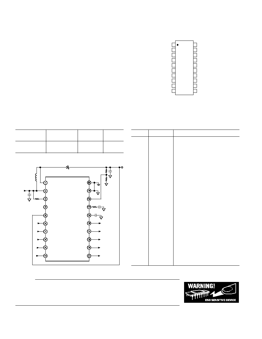
PIN CONFIGURATION
SS
COMP
SW
FB
IN
PGND
SD
VCMO
G1O
AGND
G2O
G3O
G4O
G1I
G2I
G3I
G4I
VCMI
AVCC
NC
TOP VIEW
(Not to Scale)
20
19
18
17
16
15
14
13
12
11
NC = NO CONNECT
1
2
3
4
5
6
7
8
9
10
ADP3041
NC
COMP
SW
FB
IN
PGND
SD
ADP3041
SS
VCMO
G1O
AGND
G2O
G3O
G4O
G1I
G2I
G3I
G4I
VCMI
AVCC
V
IN
C
IN
L1
R1
RSD
R
C
C
SS
R2
C
OUT
C
C
D1
Figure 1. Typical Application
PIN FUNCTION DESCRIPTIONS
Pin No.
Mnemonic
Function
1
SW
Switching Output
2
IN
Main Power Supply Input
3
SD
Shutdown Input
4
NC
No Connection
5
AVCC
Buffers Power Supply Input
6
VCMI
VCOM Buffer Input
7
G1I
Gamma 1 Buffer Input
8
G2I
Gamma 2 Buffer Input
9
G3I
Gamma 3 Buffer Input
10
G4I
Gamma 4 Buffer Input
11
G4O
Gamma 4 Buffer Output
12
G3O
Gamma 3 Buffer Output
13
G2O
Gamma 2 Buffer Output
14
G1O
Gamma 1 Buffer Output
15
VCMO
VCOM Buffer Output
16
SS
Soft Start Capacitor Timer Set
17
COMP
Compensation Input
18
FB
Feedback Voltage Sense Input
19
AGND
Analog Signal Ground
20
PGND
Ground Return for Power Transistor
ORDERING GUIDE
Temperature
Voltage
Package
Model
Range
Output
Option
ADP3041ARU
≠40
∞C to +85∞C 4.5 V to 12 V TSSOP-20
ADP3041ARUZ
* ≠40
∞C to +85∞C 4.5 V to 12 V TSSOP-20
*Z = Pb-free part.

REV. D
ADP3041
≠5≠
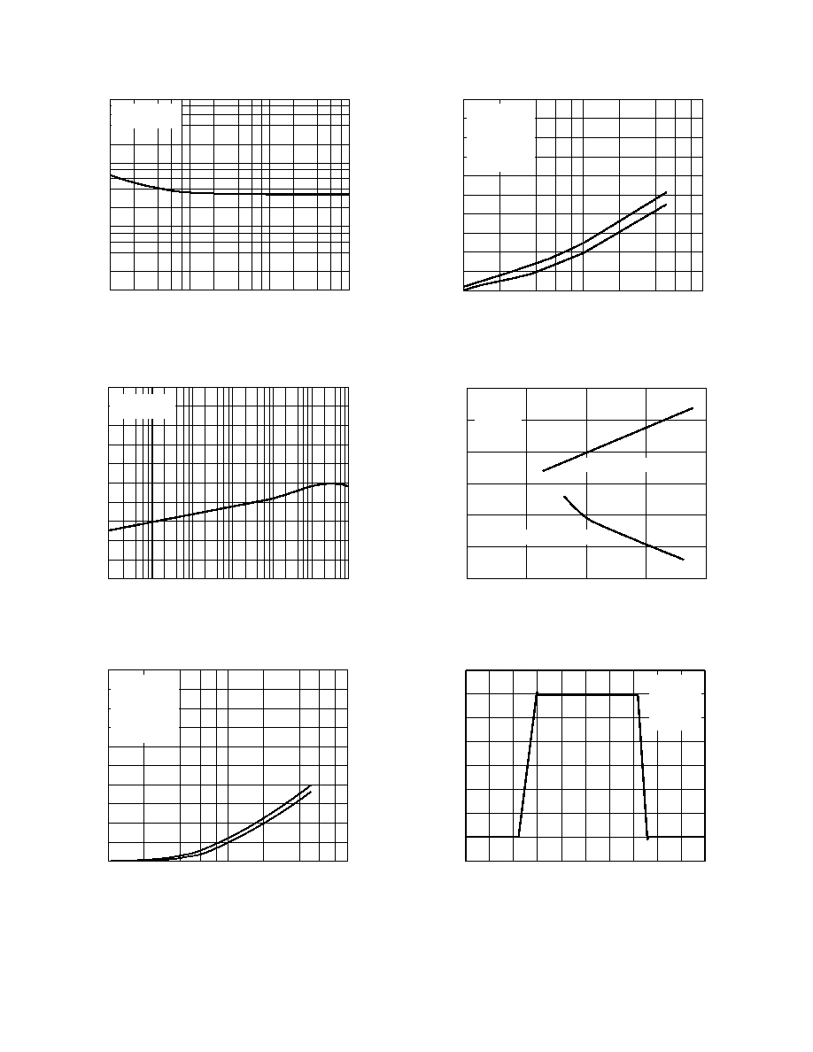
INPUT OFFSET VOLTAGE (mV)
100
0
≠12
≠9
QU
ANTITY (Amplifier
s)
≠6
≠3
0
3
6
9
12
90
50
30
20
10
80
70
40
60
T
A
= 25 C
4.5V < V
S
< 16V
TPC 1. Input Offset Voltage Distribution
TCVOS ( V/ C)
300
150
0
0
100
10
QU
ANTITY (Amplifier
s)
20
30
40
50
60
70
80
90
250
200
100
50
4.5V < V
S
< 16V
TPC 2. Input Offset Voltage Drift Distribution
TEMPERATURE ( C)
0
≠0.25
≠40
INPUT OFFSET VOLTAGE (mV)
25
85
≠0.50
≠0.75
≠1.00
≠1.25
V
CM
= V
S
/2
V
S
= 16V
V
S
= 4.5V
≠1.50
TPC 3. Input Offset Voltage vs. Temperature
Typical Performance Characteristics≠
TEMPERATURE ( C)
0
≠50
≠350
≠40
INPUT BIAS CURRENT (nA)
25
85
≠150
≠200
≠250
≠300
V
CM
= V
S
/2
V
S
= 16V
V
S
= 4.5V
≠100
TPC 4. Input Bias Current vs. Temperature
TEMPERATURE ( C)
5
≠5
≠40
INPUT OFFSET CURRENT (nA)
25
85
≠2
≠3
≠4
V
S
= 16V
V
S
= 4.5V
≠1
4
3
2
1
0
TPC 5. Input Offset Current vs. Temperature
TEMPERATURE ( C)
15.96
15.86
≠40
OUTPUT VOLTAGE SWING (V)
25
85
15.89
15.88
15.87
V
S
= 16V
V
S
= 4.5V
15.90
15.95
15.94
15.93
15.92
15.91
I
LOAD
= 5mA
4.46
4.36
4.39
4.38
4.37
4.40
4.45
4.44
4.43
4.42
4.41
TPC 6. Output Voltage Swing vs. Temperature

REV. D
≠6≠
ADP3041
TEMPERATURE ( C)
150
0
40
OUTPUT VOLTAGE SWING (mV)
25
85
45
30
15
V
S
= 16V
V
S
= 4.5V
60
135
120
105
90
75
I
LOAD
= 5mA
TPC 7. Output Voltage Swing vs. Temperature
(Small Signal)
TEMPERATURE ( C)
0.9999
0.9995
40
GAIN ERROR (V/V)
25
85
R
L
= 2k
4.5V < V
S
< 16V
V
OUT
= 0.5V TO 15V
0.9997
R
L
= 600
TPC 8. Voltage Gain vs. Temperature
LOAD CURRENT (mA)
10
0.1
0.001
100
0.01
OUTPUT V
O
L
T
A
GE
(mV)
0.1
1
10
1
100
1k
T
A
= 25 C
V
S
= 16V
V
S
= 4.5V
TPC 9. Output Voltage to Supply Rail vs. Load Current
TEMPERATURE ( C)
0.85
0.55
40
SUPPLY CURRENT/AMPLIFIER (mA)
25
85
0.70
0.65
0.60
V
S
= 16V
V
S
= 4.5V
0.75
V
CM
= V
S
/2
0.80
TPC 10. Supply Current/Amplifier vs. Temperature
TEMPERATURE ( C)
7
≠40
SLEW RATE (V/
s)
25
85
3
2
1
V
S
= 16V
V
S
= 4.5V
4
R
L
= 10k
C
L
= 200pF
5
6
8
TPC 11. Slew Rate vs. Temperature
SUPPLY VOLTAGE (V)
1.0
0
18
2
SUPPL
Y CURRENT/AMPLIFIER (mA)
4
6
8
10
12
14
16
0.9
0.5
0.3
0.2
0.1
0.8
0.7
0.4
0.6
T
A
= 25 C
A
V
= 1
V
O
= V
S
/2
1.1
TPC 12. Supply Current/Amplifier vs. Supply Voltage

REV. D
ADP3041
≠7≠
FREQUENCY (Hz)
10
≠40
100k
100M
GAIN (dB)
10M
1M
≠35
≠30
≠25
≠20
≠15
≠10
≠5
5
0
1k
10k
560
150
T
A
= 25 C
V
S
= 8V
V
IN
= 50mV rms
C
L
= 40pF
A
V
= +1
TPC 13. Resistive Loading vs. Frequency Response
FREQUENCY (Hz)
25
100k
100M
GAIN (dB)
10M
1M
≠25
≠20
≠15
≠10
≠5
20
0
1040pF
10
5
15
50pF
100pF
540pF
T
A
= 25 C
V
S
= 8V
V
IN
= 50mV rms
R
L
= 10k
A
V
= +1
TPC 14. Capacitive Loading vs. Frequency Response
FREQUENCY (Hz)
100
10M
1k
IMPED
ANCE (
)
10k
100k
1M
500
450
0
400
350
300
250
200
150
100
V
S
= 16V
V
S
= 4.5V
50
TPC 15. Closed-Loop Output Impedance vs. Frequency
OUTPUT SWING (V p-p)
FREQUENCY (Hz)
10M
1M
100k
10k
1k
100
10
0
2
4
6
8
10
12
14
16
18
T
A
= 25 C
V
S
= 16V
A
V
= +1
R
L
= 10k
DISTORTION < 1%
TPC 16. Closed-Loop Output Swing vs. Frequency
FREQUENCY (Hz)
100
10M
1k
PO
WER SUPPL
Y REJECTION RA
TIO (dB)
10k
100k
1M
160
140
≠40
120
100
80
60
40
20
0
+PSRR
≠20
PSRR
T
A
= 25 C
V
S
= 16V
TPC 17. Power Supply Rejection Ratio vs. Frequency,
V
S
= 16 V
FREQUENCY (Hz)
100
10M
1k
PO
WER SUPPL
Y REJECTION RA
TIO (dB)
10k
100k
1M
160
140
≠40
120
100
80
60
40
20
0
+PSRR
≠20
PSRR
T
A
= 25 C
V
S
= 4.5V
TPC 18. Power Supply Rejection Ratio vs. Frequency,
V
S
= 4.5 V
REV. D
≠8≠
ADP3041
FREQUENCY (Hz)
1k
100
1
10
10k
100
VO
LTA
G
E
NOISE DENSITY (nV/
Hz)
1k
10
T
A
= 25 C
4.5V
V
S
16V
TPC 19. Voltage Noise Density vs. Frequency
CHANNEL SEP
ARA
TION (dB)
FREQUENCY (Hz)
100M
10M
1M
100k
10k
1k
100
≠180
≠140
≠120
≠100
≠80
≠60
≠40
≠20
0
20
T
A
= 25 C
4.5V < V
S
< 16V
≠160
TPC 20. Channel Separation vs. Frequency
LOAD CAPACITANCE (pF)
100
90
0
10
1k
100
O
VERSHOO
T (%)
80
70
60
50
40
30
20
10
T
A
= 25 C
V
S
= 16V
V
CM
= 8V
V
IN
= 100mV p-p
A
V
= +1
R
L
= 10k
≠OS
+OS
TPC 21. Small Signal Overshoot vs. Load Capacitance,
V
S
= 16 V
LOAD CAPACITANCE (pF)
100
90
0
10
1k
100
O
VERSHOO
T (%)
80
70
60
50
40
30
20
10
T
A
= 25 C
V
S
= 4.5V
V
CM
= 2.25V
V
IN
= 100mV p-p
A
V
= +1
R
L
= 10k
≠OS
+OS
TPC 22. Small Signal Overshoot vs. Load Capacitance,
V
S
= 4.5 V
SETTLING TIME ( s)
15
10
≠15
0
2.0
0.5
OUTPUT SWING FR
OM 0V
T
O
V
1.0
1.5
5
0
≠5
≠10
T
A
= 25 C
V
S
= 8V
R
L
= 10k
OVERSHOOT SETTLING TO 0.1%
UNDERSHOOT SETTLING TO 0.1%
TPC 23. Step Size vs. Settling Time
TIME (2 s/DIV)
0
0
0
0
0
VO
LTA
GE (2V/DIV)
0
0
0
0
0
0
0
0
0
0
0
0
0
T
A
= 25 C
V
S
= 16V
A
V
= +1
R
L
= 10k
C
L
= 300pF
TPC 24. Large Signal Transient Response, V
S
= 16 V

REV. D
ADP3041
≠9≠
TIME (2 s/DIV)
0
0
0
0
0
VO
LTA
GE (1V/DIV)
0
0
0
0
0
0
0
0
0
0
0
0
0
T
A
= 25 C
V
S
= 4.5V
A
V
= +1
R
L
= 10k
C
L
= 300pF
TPC 25. Large Signal Transient Response, V
S
= 4.5 V
TIME (1 s/DIV)
0
0
0
0
0
VO
LTA
GE (50mV/DIV)
0
0
0
0
0
0
0
0
0
0
0
0
0
T
A
= 25 C
V
S
= 16V
A
V
= +1
R
L
= 10k
C
L
= 100pF
TPC 26. Small Signal Transient Response, V
S
= 16 V
TIME (1 s/DIV)
0
0
0
0
0
VO
LTA
GE (50mV/DIV)
0
0
0
0
0
0
0
0
0
0
0
0
0
T
A
= 25 C
V
S
= 4.5V
A
V
= +1
R
L
= 10k
C
L
= 100pF
TPC 27. Small Signal Transient Response, V
S
= 4.5 V
TIME (40 s/DIV)
0
0
0
0
0
VO
LTA
GE (3V/DIV)
0
0
0
0
0
0
0
0
0
0
0
0
0
T
A
= 25 C
V
S
= 16V
A
V
= +1
R
L
= 10k
TPC 28. No Phase Reversal

REV. D
≠10≠
ADP3041
THEORY OF OPERATION
Switching Regulator
The ADP3041 is a boost converter driver that stores energy
from an input voltage in an inductor and delivers that energy,
augmented by the input, to a load at a higher output voltage. It
includes a voltage reference and an error amplifier to com-
pare some fraction of the load voltage to the reference and to
amplify any difference between them. The amplified error
signal is compared to a dynamic signal produced by an inter-
nal ramp generator incorporating switch current feedback. The
comparator output timing sets the duty ratio of a switch driv-
ing the inductor to maintain the desired output voltage.
Referring to Figure 1, a typical application powers both the IC
and the inductor from the same input voltage. The on-chip
MOSFET is driven on, pulling the SW pin close to PGND. The
resulting voltage across the inductor causes its current to increase
approximately linearly, with respect to time.
When the MOSFET switch is turned off, the inductor current
cannot drop to zero, and so this current drives the SW node
capacitance rapidly positive until the diode becomes forward
biased. The inductor current now begins to charge the load
capacitor, causing a slight increase in output voltage. Generally,
the load capacitor is made large enough that this increase is very
small during the time the switch is off. During this time, inductor
current is also delivered to the load. In steady state operation,
the inductor current exceeds the load current, and the excess is
what charges the load capacitor. The inductor current falls
during this time, though not necessarily to zero.
During the next cycle, initiated by the on-chip oscillator, the
switch is again turned on so that the inductor current is ramped
up again. The charge on the load capacitor provides load current
during that interval. The remainder of the chip is arranged to
control the duty ratio of the switch to maintain a chosen output
voltage despite changes in input voltage or load current.
The output voltage is scaled down by a resistor voltage divider
and presented to the g
m
amplifier. This amplifier operates on
the difference between an on-chip reference and the voltage at
the FB pin so as to bring them to balance. This is when the
output voltage equals the reference voltage multiplied by the
resistor voltage divider ratio.
The g
m
amplifier drives an internal comparator, which has at its
other input a positive-going ramp produced by the oscillator
and modified by the current sense amplifier. The MOSFET
switch is turned on as the modified ramp voltage rises. When
this voltage exceeds the output of the g
m
amplifier, the compara-
tor turns off the switch by resetting the flip-flop previously set
by the oscillator. The output of the flip-flop is buffered by a high
current driver, which turned on the MOSFET switch at the
beginning of the oscillator cycle.
In the steady state with constant load and input voltage, the
current in the inductor cycles around some average current
level. The increasing ramp of current depends on input voltage
and t
1
, the switch-on time, while the decreasing ramp depends
on the difference between the input and output voltage and t
2
,
the remainder of the cycle. For the peaks of these two ramps
to be equal and opposite to maintain steady state, one can say
that t
1
◊ V
IN
will equal t
2
◊ (V
OUT
≠ V
IN
), if we neglect the effect
of resistance in the inductor and switch and the forward voltage
drop of the diode. From this equality one can derive t
1
/T = 1 ≠
V
IN
/V
OUT
, where T is the period of a cycle, t
1
+ t
2
. This result
gives us the switch duty ratio, t
1
/T, in terms of the input and
output voltages.
In practice, the duty ratio needs to be slightly higher than this
calculation. Because of series resistance in the inductor and the
switch, the voltage across the actual inductance is somewhat less
than the applied V
IN
, and the actual output voltage is less than
our approximation by the amount of the diode forward voltage
drop. However, the feedback control within the ADP3041 adjusts
the duty ratio to maintain the output voltage. Changes in
load current and input voltage are also accommodated by the
feedback control.
Changes in load current alone require a change in duty ratio in
order to change the average inductor current. Once the inductor
current adapts to the new load current, the duty ratio should
return to nearly its original value, as one can see from the
duty cycle calculation, which depends on input and output
voltages but not on current. Increasing the switch duty ratio
initially reduces the output voltage until the average inductor
current increases enough to offset the reduction of the t
2
interval. By limiting the duty ratio, one can prevent this effect
from regeneratively increasing the duty ratio to 100%, which
would cause the output to fall and the switch current to rise
without limit. The duty ratio is limited to about 80% by the
design of the oscillator and an additional flip-flop reset.
A comparator compares the current sense amplifier output to a
factory set limit that resets the flip-flop, turning off the switch.
This prevents runaway or overload conditions from damaging
the switch and reflecting fault overloads back to the input. Of
course, the load is directly connected to the input by way of the
diode and inductor, so protection against short circuited loads
must be done at the power input.
The g
m
amplifier has high voltage gain to ensure the output
voltage accuracy and invariance with load and input voltage.
However, because it is a g
m
amplifier with a specified current
response to input signal voltages, its high frequency response
can be controlled by the compensation impedance. This permits
the high frequency gain of the g
m
amplifier to be optimized for
the best compromise between speed of response and frequency
stability.
The stable closed-loop bandwidth of the system can be extended
by the current feedback shown. A signal representing the magni-
tude of the switch current is added to the ramp. This dynamically
reduces the duty ratio as the current in the inductor increases,
until the g
m
amplifier restores it, improving the closed-loop
frequency stability.
Soft Start
The soft start pin can load the COMP pin, forcing a low duty
cycle when its voltage is low. A capacitor on SS initially holds
the pin low; however, a small internal current charges the
capacitor, causing SS to rise after
SD goes high. As it rises,

REV. D
ADP3041
≠11≠
COMP is allowed to rise slowly until the control loop limits the
voltage to that required for regulation. SS continues to rise and
no longer affects COMP once soft start is complete.
When
SD goes low, an internal switch discharges the SS
capacitor to return its voltage to zero for soft restart.
Because of the large current that flows into the main MOSFET
switch, it is provided with a separate PGND return to the nega-
tive supply terminal to avoid corrupting the small-signal return,
GND, that can be used as a sense line at the output load point.
Buffers
This family of buffers is designed to drive large capacitive loads
in LCD applications. Each has high output current drive and
rail-to-rail input/output operation and can be powered from a
single 12 V supply. They are also intended for other applications
where low distortion and high output current drive are needed.
Input Overvoltage Protection
As with any semiconductor device, whenever the input exceeds
either supply voltage, attention needs to be paid to the input
overvoltage characteristics. As an overvoltage occurs, the ampli-
fier could be damaged, depending on the voltage level and the
magnitude of the fault current. When the input voltage exceeds
either supply by more than 0.6 V, the internal pin junctions
allow current to flow from the input to the supplies.
This input current is not inherently damaging to the device as
long as it is limited to 5 mA or less. If a condition exists using
the buffers where the input exceeds the supply more than 0.6 V,
a series external resistor should be added. The size of the resis-
tor can be calculated by using the maximum overvoltage divided
by 5 mA. This resistance should be placed in series with the
input exposed to an overvoltage.
Output Phase Reversal
The buffer family is immune to phase reversal. Although the
device's output does not change phase, large currents due to
input overvoltage could damage the device. In applications
where the possibility of an input voltage exceeding the supply
voltage exists, overvoltage protection should be used as described
in the previous section.
APPLICATION INFORMATION
Output Voltage
The ADP3041 operates with an adjustable output from V
IN
to
12 V. The output voltage is fed back to the ADP3041 via resis-
tor dividers R1 and R2 (Figure 1). The feedback voltage is
1.233 V, so the output voltage is set by the formula
V
V
R
R
OUT
=
◊ +
1.233
1
1
2
(1)
Because the feedback bias current is 100 nA maximum, R2 may
have a value up to 100 k
with minimum error due to the bias
current.
Inductor Selection
For most applications, the inductor used with the ADP3041
should be in the range of 1
µH to 22 µH. Several inductor
manufacturers are listed in Table I. When selecting an inductor,
it is important to make sure that the inductor used with the
ADP3041 is able to handle a peak current without saturation, and
that the peak current is below the current limit of the ADP3041.
Table I. Inductor Manufacturers
Part
L (
µH)
Max DCR (m
)
Height (mm)
Vendor
CMD4D11-4R7M
4.7
166
1.1
Sumida
CCDRH5D18-100
10
124
2.0
847-545-6700
CR43-4R7
4.7
109
3.5
www.sumida.com
CR43-100
10
182
3.5
DS1608-472
4.7
60
2.9
Coilcraft
DS1608-103
10
75
2.9
847-639-6400
www.coilcraft.com
D52LC-4R7M
4.7
84
2.0
Toko
D52LC-100M
10
137
2.0
847-297-0070
www.tokoam.com

REV. D
≠12≠
ADP3041
As a rule, powdered iron cores saturate softly, whereas ferrite cores
saturate abruptly. Open drum core inductors tend to saturate
gradually and are low cost and small in size, making these
types of inductors attractive in many applications. However,
care must be exercised in their placement because they have
high magnetic fields. In applications that are sensitive to mag-
netic fields, shielded geometrics are recommended.
In addition, inductor losses must be considered. Both core and
copper losses contribute to loss in converter efficiency. To mini-
mize core losses, look for inductors rated for operation at high
switching frequencies. To minimize copper losses, it is best to
use low dc resistance inductors. Typically, it is best to use an
inductor with a dc resistance lower than 20 m
per µH.
The inductor value can be estimated using
L
V
V
M
OUT
IN
SLOPE
=
(
)
◊
≠
(2)
where M
SLOPE
is the scaling factor for the proper slope compensation.
M
f
SLOPE
SW
=
1 456
.
(3)
Choose the closest standard inductor value as a starting point.
The corresponding peak inductor current can then be calculated.
I PEAK
I
V
V
V
V
V
L V
f
L
OUT
OUT
IN
IN
OUT
IN
OUT
S
(
)
=
◊
+
◊
(
)
◊
◊
1
2
≠
(4)
It is recommended to try several different inductor values, sizes,
and types to find the best inductor for the application. In gen-
eral, large inductor values lead to lower ripple current, less
output noise, and either larger size or higher dc resistance.
Conversely, low inductor values lead to higher ripple current,
more noise, and either smaller size or lower dc resistance. The
final inductor selection should be based on the best trade-off of
size, cost, and performance.
Capacitor Selection
The ADP3041 requires an input capacitor to reduce the switching
ripple and noise on the IN pin. The value of the input capaci-
tor depends on the application. For most applications, a minimum
of 10
µF is required. For applications that are running close to
current limit or that have large transient loads, input capacitors
in the range of 22
µF to 47 µF are required.
The selection of the output capacitor also depends on the
application. Given the allowable output ripple voltage, V
OUT
,
the criteria for selecting the output capacitor can be calcu-
lated using
C
I
V
V
f
V
V
OUT
OUT
OUT
IN
S
OUT
OUT
◊
(
)
◊
◊
8
≠
(5)
ESR
V
I PEAK
C
OUT
L
OUT
(
)
(6)
When selecting an output capacitor, make sure that the ripple
current rating is sufficient to cover the rms switching current
of the ADP3041. The ripple current in the output capacitor is
given by
I
C
I
V
V
V
RMS
OUT
OUT
OUT
IN
IN
(
)
=
≠
(7)
Multilayer ceramic capacitors are a good choice since they have
low ESR, high ripple current rating, and a very small package
size. Tantalum or OS-CON capacitors can be used; however,
they have a larger package size and higher ESR. Table II lists
some capacitor manufacturers. Consult the manufacturer for
more information.
Table II. Capacitor Manufacturers
Vendor
Phone No.
Web Address
AVX
843-448-9411
www.avxcorp.com
Murata
770-436-1300
www.murata.com
Sanyo
408-749-9714
www.sanyovideo.com
Taiyo Yuden
858-554-0755
www.t-yuden.com
Diode Selection
In specifying a diode, consideration must be given to speed,
forward current, forward voltage drop, reverse leakage current,
and the breakdown voltage. The output diode should be rated to
handle the maximum output current. If the output can be sub-
jected to accidental short circuits, then the diode must be rated to
handle currents up to the current limit of the ADP3041. The
breakdown rating of the diode must exceed the output voltage. A
high speed diode with low forward drop and low leakage will help
improve the efficiency of the converter by lowering the losses of
the diode. Schottky diodes are recommended.
Loop Compensation
Like most current programmed PWM converters, the ADP3041
needs compensation to maintain stability over the operating
conditions of the particular application. For operation at duty
cycles above 50%, the choice of inductor is critical in maintain-
ing stability. If the slope of the inductor current is too small or
too large, the circuit will be unstable. See the Inductor Selection
section for more information on choosing the proper inductor.
The ADP3041 provides a pin (COMP) for compensating the
voltage feedback loop. This is done by connecting a series R
C
network from the COMP pin to GND (see Figure 2). For most
applications, the compensation resistor, R
C
, should be in the
range of 5 k
< R
C
< 400 k
, and the compensation capacitor,
C
C
, in the range of 100 pF < C
C
< 10 nF. Further details for
selecting the compensation components follow.

REV. D
ADP3041
≠13≠
COMP
FB
ERROR
AMP
C2
gm
REF
C
C
R
C
Figure 2. Compensation Components
The boost regulator introduces a right half plane (RHP) zero. This
zero behaves like a zero with respect to the gain but behaves
like a pole with respect to phase. As a result, the RHP zero can
cause instability of the control loop if the bandwidth (in Hertz)
of the loop includes it.
f
RHP
V
V
R
L
Z
IN
OUT
LOAD
(
)
=
◊
◊
2
2
(8)
Note that the RHP zero is dependant on the load. To optimize
the compensation, a nominal load must be chosen. Typically,
choosing an R
LOAD
that is halfway between no load and full
load works well; but make sure that this load is enough to ensure
CCM operation. The critical value of load resistance, R
CRIT
, for
CCM is given by
R
L
f
V
V
V
V
CRIT
SW
IN
OUT
IN
OUT
=
◊ ◊
2
1
2
≠
(9)
So for the nominal load resistance R
LOAD
, use the half load
resistance or R
CRIT
, whichever is lower.
To make sure the RHP zero does not cause stability problems,
the control loop bandwidth should be set at around 1/8 the
frequency (in Hertz) of the RHP zero.
f
f
RHP
C
Z
= ◊
(
)
1
8
(10)
where f
C
is the crossover frequency.
Another frequency of interest is the pole caused by the output
load and output capacitor. This frequency (in Hertz) is calcu-
lated using
f
R
C
P
LOAD
OUT
1
1
2
=
◊
◊
(11)
Note that the frequency varies with load current. Again, use the
nominal load resistance for the calculation.
So the compensation resistor, R
C
, can be calculated by deter-
mining the open-loop gain at the crossover frequency, f
C
, and
setting R
C
to adjust the closed-loop gain to zero. The open-loop
gain can be approximated (in dB) by
G
f
V
R
V
≠
f
f
OC
C
IN
LOAD
OUT
C
P
( )
=
◊
◊
+
20
0.65
20log
1
1
2
log
(12)
R
g
V
V
C
m
FB
OUT
G
OC f C
=
◊
◊
( )
1
10
20
(13)
Once the value of the compensation resistor is determined, the
value of the compensation capacitor, C
C
, can be calculated. The
compensation capacitor sets up a zero to cancel out the pole
created by the output load, f
P1
. Since the load pole position
varies with load current, the compensation zero should be located
approximately four times the worst-case load pole, 4
◊ f
P1
, or at
one half the crossover frequency, 1/2
◊ f
C
, whichever is lower.
The frequency of the compensation zero is located at
f
R
C
ZC
C
C
=
◊ ◊
◊
1
2
(14)
So, the value of C
C
can be calculated using
C
f
R
C
ZC
C
=
◊ ◊
◊
1
2
(15)
If the output capacitor selected has a high ESR value, it may be
necessary to add another pole to cancel the zero introduced by
the capacitor's ESR. The ESR zero location is determined by
f
ESR
R
C
Z
ESR
OUT
(
)
=
◊ ◊
◊
1
2
(16)
So, a high frequency pole should be placed to cancel the ESR
zero or at half the switching frequency, whichever is lower. By
placing a pole at half the switching frequency, the high fre-
quency gain is rolled off for better phase margin. Note that the
high frequency pole must be at least a decade above the com-
pensation zero in order for the compensation to work properly.
If this is not the case, the high frequency pole should not be used.
C
C
f
R
C
C
P HF
C
C
2
1
2
=
+
◊
◊
◊
(
)
( )
(17)
After all the compensation components have been selected, the
best check for stability and response time is to observe the tran-
sient performance of the ADP3041. Adjust R
C
and C
C
as necessary
to optimize the transient response. Increasing R
C
increases

REV. D
≠14≠
ADP3041
the high frequency gain. Increasing C
C
decreases the compensa-
tion zero frequency, which increases the stability but slows the
transient response.
Shutdown
The ADP3041 shuts down to reduce the supply current to a 10
µA
maximum when the shutdown pin is pulled low. In this mode,
the internal reference, error amplifier, comparator, biasing cir-
cuitry, and the internal MOSFET switch are turned off. Note
that the output is still connected to the input via the inductor
and Schottky diode when in shutdown.
Layout Procedure
To get high efficiency, good regulation, and stability, a good
printed circuit board layout is required. It is strongly recom-
mended that the evaluation board layout be followed as closely
as possible. Use the following general guidelines when designing
printed circuit boards (see Figure 1):
1. Keep C
IN
close to the IN pin of the ADP3041.
2. Keep the high current path from C
IN
through L1 to the SW
pin and PGND pin as short as possible.
3. Similarly, keep the high current path from C
IN
through L1,
D1, and C
OUT
as short as possible.
4. Keep high current traces as short and wide as possible.
5. Place the feedback resistors as close to the FB pin as possible
to prevent noise pickup.
6. Place the compensation components as close to the COMP
pin as possible.
7. Avoid routing noise sensitive traces near the high current
traces and components.

REV. D
ADP3041
≠15≠
OUTLINE DIMENSIONS
20-Lead Thin Shrink Small Outline Package [TSSOP]
(RU-20)
Dimensions shown in millimeters
20
1
11
10
6.40 BSC
4.50
4.40
4.30
PIN 1
6.60
6.50
6.40
SEATING
PLANE
0.15
0.05
0.30
0.19
0.65
BSC
1.20
MAX
0.20
0.09
0.75
0.60
0.45
8
0
COMPLIANT TO JEDEC STANDARDS MO-153AC
COPLANARITY
0.10

REV. D
C03361≠0≠12/03(D)
≠16≠
ADP3041
Revision History
Location
Page
12/03--Data Sheet changed from REV. C to REV. D.
Updated ORDERING GUIDE . . . . . . . . . . . . . . . . . . . . . . . . . . . . . . . . . . . . . . . . . . . . . . . . . . . . . . . . . . . . . . . . . . . . . . . . . . . . . 4
Updated formatting of Typical Performance Characteristics . . . . . . . . . . . . . . . . . . . . . . . . . . . . . . . . . . . . . . . . . . . . . . . . . . . . . . . 5
Change to TPC 1 . . . . . . . . . . . . . . . . . . . . . . . . . . . . . . . . . . . . . . . . . . . . . . . . . . . . . . . . . . . . . . . . . . . . . . . . . . . . . . . . . . . . . . . 5
Changes to Table I . . . . . . . . . . . . . . . . . . . . . . . . . . . . . . . . . . . . . . . . . . . . . . . . . . . . . . . . . . . . . . . . . . . . . . . . . . . . . . . . . . . . . 11
Changes to Table II . . . . . . . . . . . . . . . . . . . . . . . . . . . . . . . . . . . . . . . . . . . . . . . . . . . . . . . . . . . . . . . . . . . . . . . . . . . . . . . . . . . . . 12
5/03--Data Sheet changed from REV. B to REV. C.
Replaced all TPCs . . . . . . . . . . . . . . . . . . . . . . . . . . . . . . . . . . . . . . . . . . . . . . . . . . . . . . . . . . . . . . . . . . . . . . . . . . . . . . . . . . . . . . . 5
Updated OUTLINE DIMENSIONS . . . . . . . . . . . . . . . . . . . . . . . . . . . . . . . . . . . . . . . . . . . . . . . . . . . . . . . . . . . . . . . . . . . . . . . 15
10/02--Data Sheet changed from REV. A to REV. B.
Updated Features . . . . . . . . . . . . . . . . . . . . . . . . . . . . . . . . . . . . . . . . . . . . . . . . . . . . . . . . . . . . . . . . . . . . . . . . . . . . . . . . . . . . . . . 1
Removed RT Pin . . . . . . . . . . . . . . . . . . . . . . . . . . . . . . . . . . . . . . . . . . . . . . . . . . . . . . . . . . . . . . . . . . . . . . . . . . . . . . . . . . . . . . . . 4