 | –≠–ª–µ–∫—Ç—Ä–æ–Ω–Ω—ã–π –∫–æ–º–ø–æ–Ω–µ–Ω—Ç: ADP3120A | –°–∫–∞—á–∞—Ç—å:  PDF PDF  ZIP ZIP |
Document Outline
- ˛ˇ
- ˛ˇ
- ˛ˇ
- ˛ˇ
- ˛ˇ
- ˛ˇ
- ˛ˇ
- ˛ˇ
- ˛ˇ
- ˛ˇ
- ˛ˇ
- ˛ˇ
- ˛ˇ
Dual Bootstrapped, 12 V MOSFET
Driver with Output Disable
ADP3120A
Rev. 0
Information furnished by Analog Devices is believed to be accurate and reliable. However, no
responsibility is assumed by Analog Devices for its use, nor for any infringements of patents or other
rights of third parties that may result from its use. Specifications subject to change without notice. No
license is granted by implication or otherwise under any patent or patent rights of Analog Devices.
Trademarks and registered trademarks are the property of their respective owners.
One Technology Way, P.O. Box 9106, Norwood, MA 02062-9106, U.S.A.
Tel: 781.329.4700
www.analog.com
Fax: 781.461.3113
©2006 Analog Devices, Inc. All rights reserved.
FEATURES
All-in-one synchronous buck driver
Bootstrapped high-side drive
One PWM signal generates both drives
Anticross conduction protection circuitry
OD for disabling the driver outputs
Meets CPU VR requirement when used with
Analog Devices Flex -ModeTM
1
controller
APPLICATIONS
Multiphase desktop CPU supplies
Single-supply synchronous buck converters
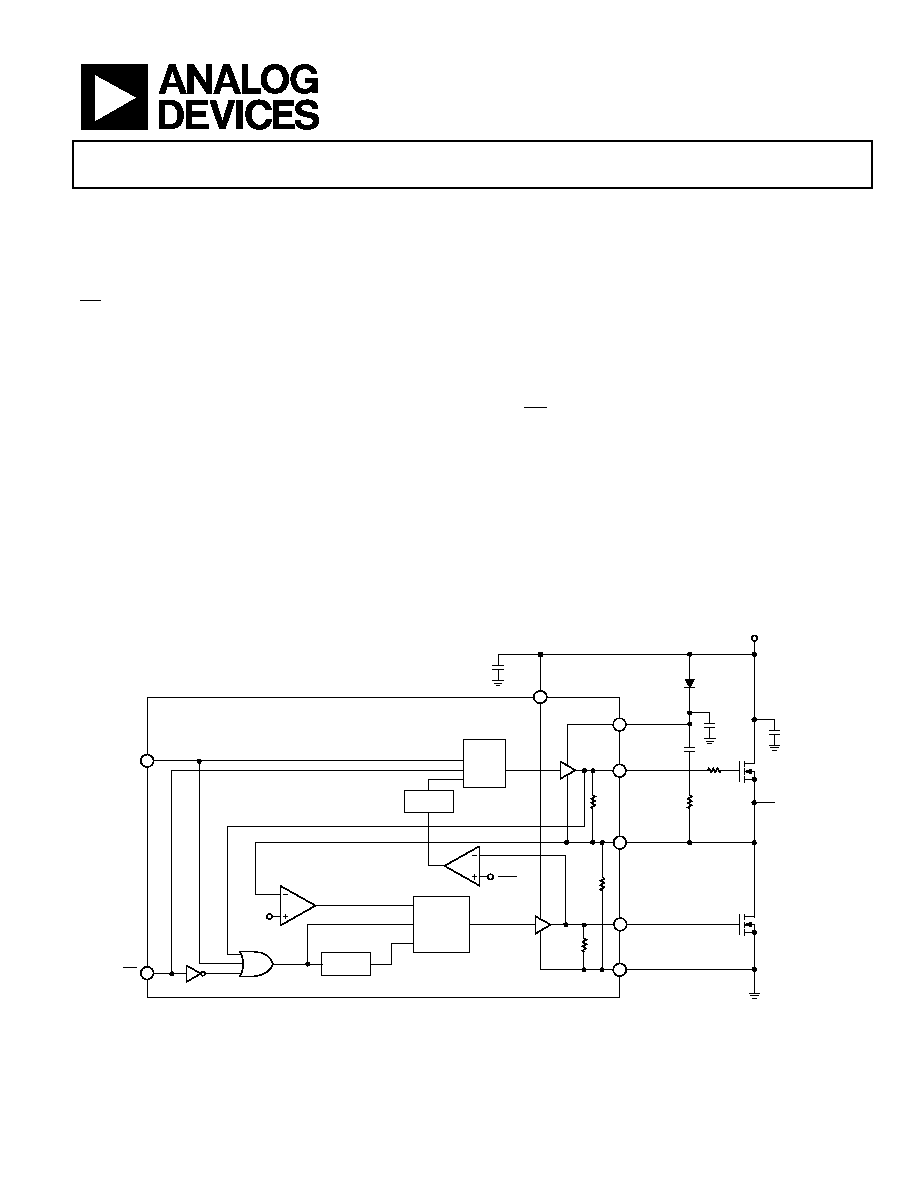
GENERAL DESCRIPTION
The ADP3120A is a dual, high voltage MOSFET driver
optimized for driving two N-channel MOSFETs, the two switches
in a nonisolated synchronous buck power converter. Each
driver is capable of driving a 3000 pF load with a 45 ns propaga-
tion delay and a 25 ns transition time. One of the drivers can be
bootstrapped and is designed to handle the high voltage slew
rate associated with floating high-side gate drivers. The
ADP3120A includes overlapping drive protection to prevent
shoot-through current in the external MOSFETs.
The OD pin shuts off both the high-side and the low-side
MOSFETs to prevent rapid output capacitor discharge during
system shutdown.
The ADP3120A is specified over the commercial temperature
range of 0∞C to 85∞C and is available in 8-lead SOIC_N and
8-lead LFCSP_VD packages.
1
Flex-Mode is protected by U.S. Patent 6683441; other patents pending.
FUNCTIONAL BLOCK DIAGRAM
2
3
OD
IN
ADP3120A
VCC
BST
DRVH
SW
DRVL
PGND
DELAY
VCC
6
DELAY
CMP
CMP
1V
4
1
7
CONTROL
LOGIC
6
5
8
R
BST
R
G
C
BST1
D1
C
BST2
12V
Q1
TO
INDUCTOR
Q2
R1
LATCH
R2
Q
S
05812-001
Figure 1.

ADP3120A
Rev. 0 | Page 2 of 16
TABLE OF CONTENTS
Features .............................................................................................. 1
Applications....................................................................................... 1
General Description ......................................................................... 1
Functional Block Diagram .............................................................. 1
Revision History ............................................................................... 2
Specifications..................................................................................... 3
Absolute Maximum Ratings............................................................ 4
ESD Caution.................................................................................. 4
Pin Configurations and Function Descriptions ........................... 5
Timing Characteristics..................................................................... 6
Typical Performance Characteristics ............................................. 7
Theory of Operation ........................................................................ 9
Low-Side Driver ............................................................................9
High-Side Driver ...........................................................................9
Overlap Protection Circuit...........................................................9
Application Information................................................................ 10
Supply Capacitor Selection ....................................................... 10
Bootstrap Circuit........................................................................ 10
MOSFET Selection..................................................................... 10
High-Side (Control) MOSFETs................................................ 10
Low-Side (Synchronous) MOSFETs ........................................ 11
PC Board Layout Considerations............................................. 11
Outline Dimensions ....................................................................... 13
Ordering Guide .......................................................................... 13
REVISION HISTORY
3/06--Revision 0: Initial Version
ADP3120A
Rev. 0 | Page 3 of 16
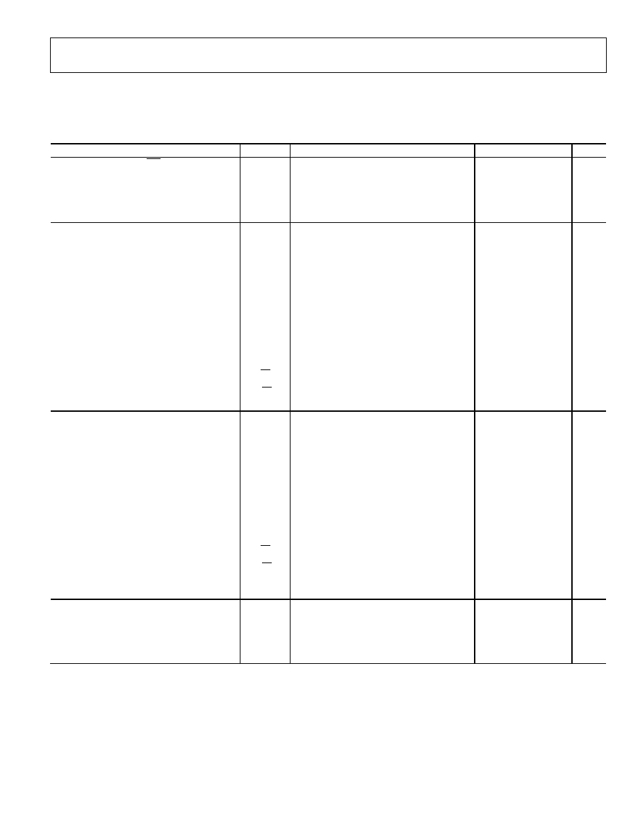
SPECIFICATIONS
V
CC
= 12 V, BST = 4 V to 26 V, T
A
= 0∞C to 85∞C, unless otherwise noted.
1
Table 1.
Parameter
Symbol Conditions
Min Typ Max Unit
DIGITAL INPUTS (PWM, OD)
Input Voltage High
2.0
V
Input Voltage Low
0.8
V
Input Current
-1
+1
A
Hysteresis
90
250
mV
HIGH-SIDE DRIVER
Output Resistance, Sourcing Current
BST - SW = 12 V ; T
A
= 25∞C
3.3
BST - SW = 12 V ; T
A
= 0∞C to 85∞C
2.5
3.9
Output Resistance, Sinking Current
BST ≠ SW = 12 V; T
A
= 25∞C
1.8
BST - SW = 12 V; T
A
= 0∞C to 85∞C
1.4
2.6
Output Resistance, Unbiased
BST ≠ SW = 0 V
10
k
Transition Times
t
rDRVH
BST ≠ SW = 12 V, C
LOAD
= 3 nF, see Figure 5
25
40
ns
t
fDRVH
BST ≠ SW = 12 V, C
LOAD
= 3 nF, see Figure 5
20
30
ns
Propagation Delay Times
t
pdhDRVH
BST ≠ SW = 12 V, C
LOAD
= 3 nF,
32
45
70
ns
25∞C
T
A
85∞C, see Figure 5
t
pdlDRVH
BST ≠ SW = 12 V, C
LOAD
= 3 nF, see Figure 5
25
35
ns
OD
pdl
t
See Figure 4
20
35
ns
OD
pdh
t
See Figure 4
40
55
ns
SW Pull-Down Resistance
SW to PGND
10
k
LOW-SIDE DRIVER
Output Resistance, Sourcing Current
T
A
= 25∞C
3.3
T
A
= 0∞C to 85∞C
2.4
3.9
Output Resistance, Sinking Current
T
A
= 25∞C
1.8
T
A
= 0∞C to 85∞C
1.4
2.6
Output Resistance, Unbiased
V
CC
= PGND
10
k
Transition Times
t
rDRVL
C
LOAD
= 3 nF, see Figure 5
20
35
ns
t
fDRVL
C
LOAD
= 3 nF, see Figure 5
16
30
ns
Propagation Delay Times
t
pdhDRVL
C
LOAD
= 3 nF, see Figure 5
12
35
ns
t
pdlDRVL
C
LOAD
= 3 nF, see Figure 5
30
45
ns
OD
pdl
t
See Figure 4
20
35
ns
OD
pdh
t
See Figure 4
110 190
ns
Timeout Delay
SW = 5 V
110
190
ns
SW = PGND
95
150
ns
SUPPLY
Supply Voltage Range
V
CC
4.15
13.2
V
Supply Current
I
SYS
BST = 12 V, IN = 0 V
2
5
mA
UVLO Voltage
V
CC
rising
1.5
3.0
V
Hysteresis
350
mV
1
All limits at temperature extremes are guaranteed via correlation using standard statistical quality control (SQC) methods.
ADP3120A
Rev. 0 | Page 4 of 16
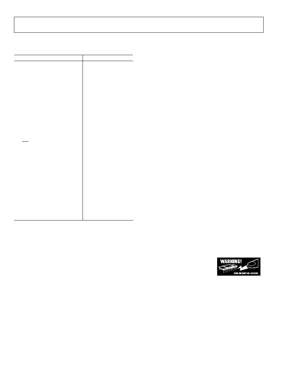
ABSOLUTE MAXIMUM RATINGS
Table 2.
Parameter Rating
VCC
-0.3 V to +15 V
BST
DC
-0.3 V to V
CC
+ 15 V
<200 ns
-0.3 V to +35 V
BST to SW
-0.3 V to +15 V
SW
DC
-5 V to +15 V
<200 ns
-10 V to +25 V
DRVH
DC
SW - 0.3 V to BST + 0.3 V
<200 ns
SW - 2 V to BST + 0.3 V
DRVL
DC -0.3
V
to
V
CC
+ 0.3 V
<200 ns
-2 V to V
CC
+ 0.3 V
IN, OD
-0.3 V to +6.5 V
JA
, SOIC_N
2-Layer Board
123∞C/W
4-Layer Board
90∞C/W
JA
, LFCSP_VD
1
4-Layer Board
50∞C/W
Operating Ambient Temperature
Range
0∞C to 85∞C
Junction Temperature Range
0∞C to 150∞C
Storage Temperature Range
-65∞C to +150∞C
Lead Temperature
Soldering (10 sec)
300∞C
Vapor Phase (60 sec)
215∞C
Infrared (15 sec)
260∞C
1
For LFCSP_VD,
JA
is measured per JEDEC STD with exposed pad soldered to PCB.
Stresses above those listed under Absolute Maximum Ratings
may cause permanent damage to the device. This is a stress
rating only; functional operation of the device at these or any
other conditions above those listed in the operational sections
of this specification is not implied. Exposure to absolute
maximum rating conditions for extended periods may affect
device reliability.
Unless otherwise specified, all voltages are referenced to PGND.
ESD CAUTION
ESD (electrostatic discharge) sensitive device. Electrostatic charges as high as 4000 V readily accumulate on
the human body and test equipment and can discharge without detection. Although this product features
proprietary ESD protection circuitry, permanent damage may occur on devices subjected to high energy
electrostatic discharges. Therefore, proper ESD precautions are recommended to avoid performance
degradation or loss of functionality.
ADP3120A
Rev. 0 | Page 5 of 16
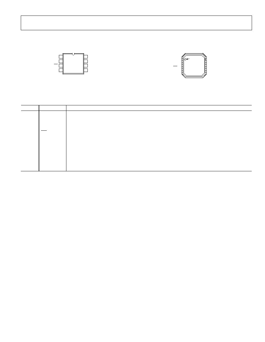
PIN CONFIGURATIONS AND FUNCTION DESCRIPTIONS
BST
1
IN
2
OD
3
VCC
4
DRVH
8
SW
7
PGND
6
DRVL
5
ADP3120A
TOP VIEW
(Not to Scale)
05812-002
Figure 2. 8-Lead SOIC_N Pin Configuration
PIN 1
INDICATOR
1
BST
2
IN
3
OD
4
VCC
7 SW
8 DRVH
6 PGND
5 DRVL
TOP VIEW
(Not to Scale)
ADP3120A
05812-003
Figure 3. 8-Lead LFCSP_VD Pin Configuration
Table 3. Pin Function Descriptions
Pin No.
Mnemonic
Description
1 BST
Upper MOSFET Floating Bootstrap Supply. A capacitor connected between the BST and SW pins holds this
bootstrapped voltage for the high-side MOSFET while it is switching.
2 IN
Logic Level PWM Input. This pin has primary control of the drive outputs. In normal operation, pulling this pin
low turns on the low-side driver; pulling it high turns on the high-side driver.
3
OD
Output Disable. When low, this pin disables normal operation, forcing DRVH and DRVL low.
4
VCC
Input Supply. This pin should be bypassed to PGND with an ~1 F ceramic capacitor.
5
DRVL
Synchronous Rectifier Drive. Output drive for the lower (synchronous rectifier) MOSFET.
6
PGND
Power Ground. This pin should be closely connected to the source of the lower MOSFET.
7 SW
Switch Node Connection. This pin is connected to the buck switching node, close to the upper MOSFET source.
It is the floating return for the upper MOSFET drive signal. It is also used to monitor the switched voltage to
prevent the lower MOSFET from turning on until the voltage is below ~1 V.
8
DRVH
Buck Drive. Output drive for the upper (buck) MOSFET.
ADP3120A
Rev. 0 | Page 6 of 16
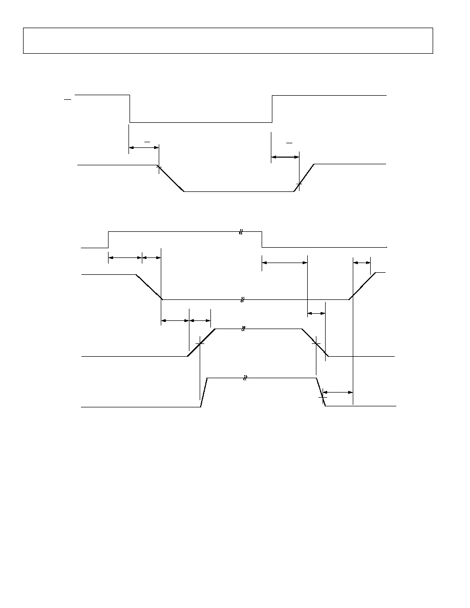
TIMING CHARACTERISTICS
Timing is referenced to the 90% and 10% points, unless otherwise noted.
t
pdlOD
90%
10%
OD
DRVH
OR
DRVL
05812-004
t
pdhOD
Figure 4. Output Disable Timing Diagram
IN
DRVH-SW
DRVL
SW
V
TH
V
TH
1V
05812-005
t
pdlDRVL
t
fDRVL
t
pdlDRVH
t
rDRVL
t
fDRVH
t
pdhDRVH
t
rDRVH
t
pdhDRVL
Figure 5. Timing Diagram

ADP3120A
Rev. 0 | Page 7 of 16
TYPICAL PERFORMANCE CHARACTERISTICS
DRVH
DRVL
IN
05812-006
Figure 6. DRVH Rise and DRVL Fall Times
C
LOAD
= 6 nF for DRVL, C
LOAD
= 2 nF for DRVH
05812-007
DRVH
DRVL
IN
Figure 7. DRVH Fall and DRVL Rise Times
C
LOAD
= 6 nF for DRVL, C
LOAD
= 2 nF for DRVH
35
15
0
125
JUNCTION TEMPERATURE (
∞
C)
R
ISE TIM
E (
n
s)
30
25
20
25
50
75
100
DRVL
DRVH
V
CC
= 12V
C
LOAD
= 3nF
05812-008
Figure 8. DRVH and DRVL Rise Times vs. Temperature
24
14
0
125
JUNCTION TEMPERATURE (
∞
C)
FALL TIME (ns)
22
20
18
16
25
50
75
100
DRVL
DRVH
V
CC
= 12V
C
LOAD
= 3nF
05812-009
Figure 9. DRVH and DRVL Fall Times vs. Temperature
40
5
2.0
5.0
LOAD CAPACITANCE (nF)
R
I
SE TIM
E (
n
s)
35
30
25
20
15
10
2.5
3.0
3.5
4.0
4.5
T
A
= 25
∞
C
V
CC
= 12V
DRVH
DRVL
05812-010
Figure 10. DRVH and DRVL Rise Times vs. Load Capacitance
35
5
2.0
5.0
LOAD CAPACITANCE (nF)
FALL TIME (ns)
30
25
20
15
10
2.5
3.0
3.5
4.0
4.5
V
CC
= 12V
T
A
= 25
∞
C
DRVH
DRVL
05812-011
Figure 11. DRVH and DRVL Fall Times vs. Load Capacitance

ADP3120A
Rev. 0 | Page 8 of 16
60
0
0
FREQUENCY (kHz)
S
U
P
P
L
Y
CURRE
NT (mA)
45
30
15
200
400
600
800
1000
1200
1400
T
A
= 25
∞
C
V
CC
= 12V
C
LOAD
= 3nF
05812-012
Figure 12. Supply Current vs. Frequency
13
9
0
125
JUNCTION TEMPERATURE (
∞
C)
S
U
P
P
L
Y
CURRE
NT (mA)
12
11
10
25
50
75
100
V
CC
= 12V
C
LOAD
= 3nF
f
IN
= 250kHz
05812-013
Figure 13. Supply Current vs. Temperature
12
0
0
1
V
CC
(V)
DRVL OUTPUT VOLTAGE (V)
2
11
10
9
8
7
6
5
4
3
2
1
1
2
3
4
5
6
7
8
9
10
11
T
A
= 25
∞
C
C
LOAD
= 3nF
05812-014
Figure 14. DRVL Output Voltage vs. Supply Voltage

ADP3120A
Rev. 0 | Page 9 of 16
THEORY OF OPERATION
The ADP3120A is optimized for driving two N-channel
MOSFETs in a synchronous buck converter topology. A single
PWM input signal is all that is required to properly drive the
high-side and the low-side MOSFETs. Each driver is capable of
driving a 3 nF load at speeds up to 500 kHz. A functional block
diagram of ADP3120A is shown in Figure 1.
LOW-SIDE DRIVER
The low-side driver is designed to drive a ground referenced
N-channel MOSFET. The bias to the low-side driver is
internally connected to the V
CC
supply and PGND.
When the driver is enabled, the driver output is 180∞ out of
phase with the PWM input. When the ADP3120A is disabled,
the low-side gate is held low.
HIGH-SIDE DRIVER
The high-side driver is designed to drive a floating N-channel
MOSFET. The bias voltage for the high-side driver is developed
by an external bootstrap supply circuit that is connected
between the BST and SW pins.
The bootstrap circuit comprises Diode D1 and Bootstrap
Capacitor C
BST1
. C
BST2
and R
BST
are included to reduce the high-
side gate drive voltage and to limit the switch node slew rate
(called a Boot-SnapTM circuit--see the Application Information
section for more details). When the ADP3120A starts up, the
SW pin is at ground, so the bootstrap capacitor charges up to
V
CC
through D1. When the PWM input goes high, the high-side
driver begins to turn on the high-side MOSFET, Q1, by pulling
charge out of C
BST1
and C
BST2
. As Q1 turns on, the SW pin rises
up to V
IN
and forces the BST pin to V
IN
+ V
C (BST)
. This holds Q1
on because enough gate-to-source voltage is provided. To complete
the cycle, Q1 is switched off by pulling the gate down to the
voltage at the SW pin. When the low-side MOSFET, Q2, turns
on, the SW pin is pulled to ground. This allows the bootstrap
capacitor to charge up to V
CC
again.
The output of the high-side driver is in phase with the PWM
input. When the driver is disabled, the high-side gate is held low.
OVERLAP PROTECTION CIRCUIT
The overlap protection circuit prevents both of the main power
switches, Q1 and Q2, from being on at the same time. This is
done to prevent shoot-through currents from flowing through
both power switches and the associated losses that can occur
during their on/off transitions. The overlap protection circuit
accomplishes this by adaptively controlling the delay from the
Q1 turn-off to the Q2 turn-on, and by internally setting the
delay from the Q2 turn-off to the Q1 turn-on.
To prevent the overlap of the gate drives during the Q1 turn-off
and the Q2 turn-on, the overlap circuit monitors the voltage at
the SW pin. When the PWM input signal goes low, Q1 begins
to turn off (after propagation delay). Before Q2 can turn on, the
overlap protection circuit makes sure that SW has first gone
high and then waits for the voltage at the SW pin to fall from
V
IN
to 1 V. Once the voltage on the SW pin falls to 1 V, Q2
begins turn-on. If the SW pin has not gone high first, the Q2
turn-on is delayed by a fixed 150 ns. By waiting for the voltage
on the SW pin to reach 1 V or for the fixed delay time, the
overlap protection circuit ensures that Q1 is off before Q2 turns
on, regardless of variations in temperature, supply voltage, input
pulse width, gate charge, and drive current. If SW does not go
below 1 V after 190 ns, DRVL turns on. This can occur if the
current flowing in the output inductor is negative and flows
through the high-side MOSFET body diode.

ADP3120A
Rev. 0 | Page 10 of 16
APPLICATION INFORMATION
SUPPLY CAPACITOR SELECTION
For the supply input (V
CC
) of the ADP3120A, a local bypass
capacitor is recommended to reduce the noise and to supply
some of the peak currents that are drawn. Use a 4.7 F, low ESR
capacitor. Multilayer ceramic chip (MLCC) capacitors provide
the best combination of low ESR and small size. Keep the
ceramic capacitor as close as possible to the ADP3120A.
BOOTSTRAP CIRCUIT
The bootstrap circuit uses a charge storage capacitor (C
BST
)
and a diode, as shown in Figure 1. These components can be
selected after the high-side MOSFET is chosen. The bootstrap
capacitor must have a voltage rating that can handle twice the
maximum supply voltage. A minimum 50 V rating is
recommended. The capacitor values are determined by
GATE
GATE
BST2
BST1
V
Q
C
C
◊
=
+
10
(1)
D
CC
GATE
BST2
BST1
BST1
V
V
V
C
C
C
-
=
+
(2)
where:
Q
GATE
is the total gate charge of the high-side MOSFET at V
GATE
.
V
GATE
is the desired gate drive voltage (usually in the range of
5 V to 10 V, 7 V being typical).
V
D
is the voltage drop across D1.
Rearranging Equation 1 and Equation 2 to solve for C
BST1
yields
D
CC
GATE
BST1
V
V
Q
C
-
◊
= 10
C
BST2
can then be found by rearranging Equation 1
1
10
BST
GATE
GATE
BST2
C
V
Q
C
-
◊
=
For example, an NTD60N02 has a total gate charge of about
12 nC at V
GATE
= 7 V. Using V
CC
= 12 V and V
D
= 1 V, then
C
BST1
= 12 nF and C
BST2
= 6.8 nF. Good quality ceramic capacitors
should be used.
R
BST
is used to limit slew rate and minimize ringing at the switch
node. It also provides peak current limiting through D1. An
R
BST
value of 1.5 to 2.2 is a good choice. The resistor needs
to handle at least 250 mW due to the peak currents that flow
through it.
A small signal diode can be used for the bootstrap diode due
to the ample gate drive voltage supplied by V
CC
. The bootstrap
diode must have a minimum 15 V rating to withstand the
maximum supply voltage. The average forward current can
be estimated by
MAX
GATE
AVG
F
f
Q
I
◊
=
)
(
(3)
where
f
MAX
is the maximum switching frequency of the
controller.
The peak surge current rating should be calculated by
BST
D
CC
PEAK
F
R
V
V
I
-
=
)
(
(4)
MOSFET SELECTION
When interfacing the ADP3120A to external MOSFETs, the
designer should consider ways to make a robust design that
minimizes stresses on both the driver and the MOSFETs. These
stresses include exceeding the short time duration voltage
ratings on the driver pins as well as the external MOSFET.
It is also highly recommended to use the Boot-Snap circuit to
improve the interaction of the driver with the characteristics of
the MOSFETs. If a simple bootstrap arrangement is used, make
sure to include a proper snubber network on the SW node.
HIGH-SIDE (CONTROL) MOSFETS
A high-side, high speed MOSFET is usually selected to
minimize switching losses (see the
ADP3186
or
ADP3188
data sheet for Flex-Mode controller details). This typically
implies a low gate resistance and low input capacitance/charge
device. Yet, a significant source lead inductance can also exist
that depends mainly on the MOSFET package; it is best to
contact the MOSFET vendor for this information.
The ADP3120A DRVH output impedance and the input
resistance of the MOSFETs determine the rate of charge delivery
to the internal capacitance of the gate. This determines the
speed at which the MOSFETs turn on and off. However, because
of potentially large currents flowing in the MOSFETs at the on
and off times (this current is usually larger at turn-off due to
ramping up of the output current in the output inductor), the
source lead inductance generates a significant voltage when the
high-side MOSFETs switch off. This creates a significant drain-
source voltage spike across the internal die of the MOSFETs and
can lead to a catastrophic avalanche. The mechanisms involved
in this avalanche condition are referenced in literature from the
MOSFET suppliers.
ADP3120A
Rev. 0 | Page 11 of 16
The MOSFET vendor should provide a rating for the maximum
voltage slew rate at drain current around which this can be
designed. Once this specification is obtained, determine the
maximum current expected in the MOSFET by
(
)
OUT
MAX
MAX
OUT
CC
DC
MAX
L
f
D
V
V
phase
per
I
I
◊
◊
-
+
=
)
(
(5)
where:
D
MAX
is determined for the VR controller being used with
the driver. This current is divided roughly equally between
MOSFETs if more than one is used (assume a worst-case
mismatch of 30% for design margin).
L
OUT
is the output inductor value.
When producing the design, there is no exact method for
calculating the dV/dt due to the parasitic effects in the external
MOSFETs as well as the PCB. However, it can be measured to
determine if it is safe. If it appears that the dV/dt is too fast, an
optional gate resistor can be added between DRVH and the
high-side MOSFETs. This resistor slows down the dV/dt, but it
increases the switching losses in the high-side MOSFETs. The
ADP3120A is optimally designed with an internal drive
impedance that works with most MOSFETs to switch them
efficiently, yet minimizes dV/dt. However, some high speed
MOSFETs can require this external gate resistor depending on
the currents being switched in the MOSFET.
LOW-SIDE (SYNCHRONOUS) MOSFETS
The low-side MOSFETs are usually selected to have a low on
resistance to minimize conduction losses. This usually implies a
large input gate capacitance and gate charge. The first concern is
to make sure the power delivery from the ADP3120A DRVL
does not exceed the thermal rating of the driver (see the
ADP3186
,
ADP3188
, or
ADP3189
data sheets for Flex-Mode
controller details).
The next concern for the low-side MOSFETs is to prevent
them from being inadvertently switched on when the high-side
MOSFET turns on. This occurs due to the drain-gate (Miller
capacitance, also specified as C
rss
capacitance) of the MOSFET.
When the drain of the low-side MOSFET is switched to V
CC
by
the high-side turning on (at a dV/dt rate), the internal gate of
the low-side MOSFET is pulled up by an amount roughly equal
to V
CC
◊ (C
rss
/C
iss
). It is important to make sure this does not put
the MOSFET into conduction.
Another consideration is the nonoverlap circuitry of the
ADP3120A that attempts to minimize the nonoverlap period.
During the state of the high-side turning off to low-side turning
on, the SW pin is monitored (as well as the conditions of SW
prior to switching) to adequately prevent overlap.
However, during the low-side turn-off to high-side turn-on,
the SW pin does not contain information for determining
the proper switching time, so the state of the DRVL pin is
monitored to go below one sixth of V
CC
; then, a delay is added.
Due to the Miller capacitance and internal delays of the low-
side MOSFET gate, ensure that the Miller-to-input capacitance
ratio is low enough, and that the low-side MOSFET internal
delays are not so large as to allow accidental turn-on of the low-
side when the high-side turns on.
Contact ADI for an updated list of recommended low-side
MOSFETs.
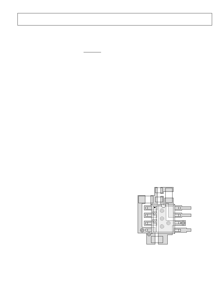
PC BOARD LAYOUT CONSIDERATIONS
Use these general guidelines when designing printed circuit
boards:
∑
Trace out the high current paths and use short, wide
(>20 mil) traces to make these connections.
∑
Minimize trace inductance between DRVH and DRVL
outputs and MOSFET gates.
∑
Connect the PGND pin of the ADP3120A as closely as
possible to the source of the lower MOSFET.
∑
Locate the V
CC
bypass capacitor as close as possible to
the VCC and PGND pins.
∑
Use vias to other layers, when possible, to maximize
thermal conduction away from the IC.
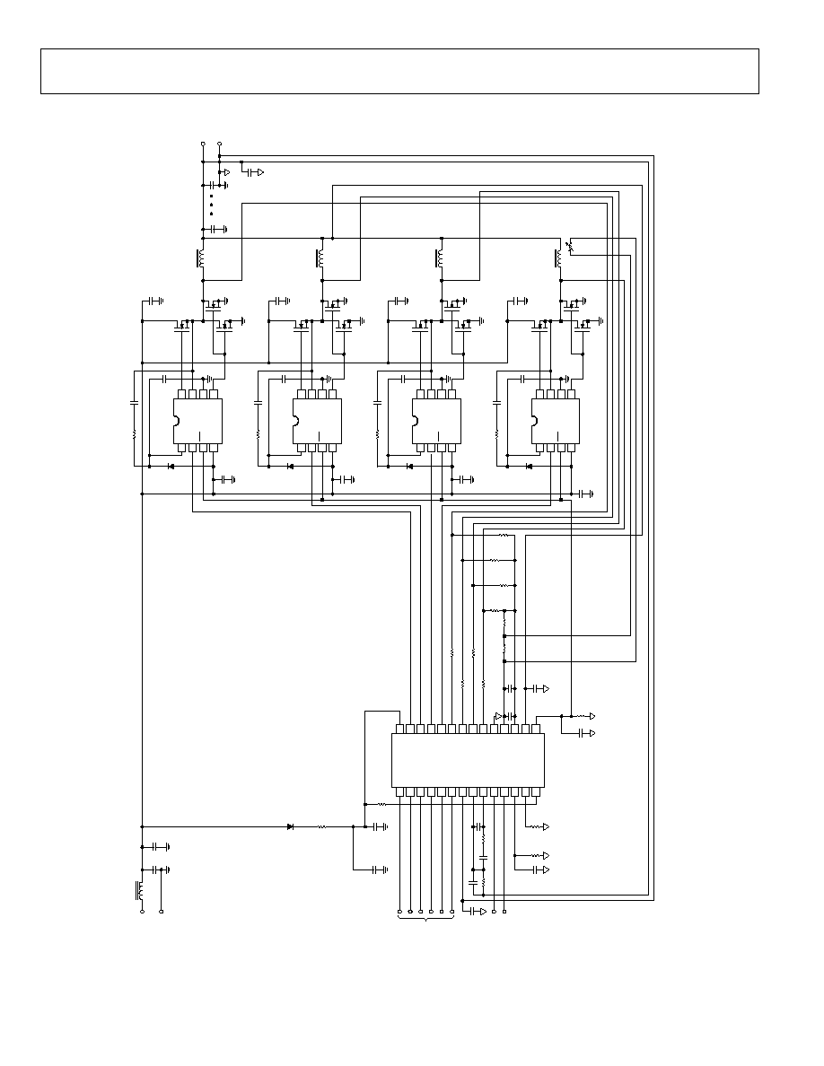
The circuit in Figure 16 shows how four drivers can be
combined with an
ADP3188
to form a total power conver-
sion solution for generating V
CC (CORE)
for an Intel CPU that is
VRD 10.x-compliant.
Figure 15 shows an example of the typical land patterns based
on the guidelines given previously. For more detailed layout
guidelines for a complete CPU voltage regulator subsystem,
refer to the PC Board Layout Considerations section of the
ADP3188
data sheet.
D1
C
BST2
C
BST1
R
BST
C
VCC
05812-015
Figure 15. External Component Placement Example
ADP3120A
Rev. 0 | Page 12 of 16
1
2
3
4
5
6
7
8
9
10
11
12
13
14
28
27
26
25
24
23
22
21
20
19
18
17
16
15
D5
1N
4148
C1
9
4.7
F
Q1
3
N
T
D
60N
02
Q1
5
N
T
D
110N
02
Q1
6
N
T
D
110N
02
C
186.8nF
C1
7
4.7
F
U5
A
D
P
3120A
BST
1
IN
2
3
VCC
4
DRVH
SW
PGND
DRVL
8
7
6
5
L5
320nH/1.4m
RTH1
100k
, 5%
NTC
R6
2.2
C2
0
12nF
D4
1N
4148
C1
5
4.7
F
Q9
N
T
D
60N
02
Q1
1
N
T
D
110N
02
Q1
2
N
T
D
110N
02
C1
4
6.8nF
C1
3
4.7
F
U4
A
D
P
3120A
BST
1
IN
2
3
VCC
4
DRVH
SW
PGND
DRVL
8
7
6
5
L4
320nH/1.4m
R5
2.2
C1
6
12nF
D3
1N
4148
C1
1
4.7
F
Q5
N
T
D
60N
02
Q7
N
T
D
110N
02
Q8
N
T
D
110N
02
C1
0
6.8nF
C9
4.7
F
U3
A
D
P
3120A
BST
1
IN
2
3
VCC
4
DRVH
SW
PGND
DRVL
8
7
6
5
D1
1N
4148
L3
320nH/1.4m
R4
2.2
C1
2
12nF
D2
1N
4148
C7
4.7
F
Q1
N
T
D
60N
02
Q3
N
T
D
110N
02
Q4
N
T
D
110N
02
C6
6.8nF
C5
4.7
F
U2
A
D
P
3120A
BST
1
IN
2
3
VCC
4
DRVH
SW
PGND
DRVL
8
7
6
5
L2
320nH/1.4m
R3
2.2
C8
12nF
+
+
C2
4
C3
1
10
F
◊
18
MLCC IN
SOCKET
V
CC (
CO
RE
)
0.8375V
≠ 1.6V
95A
TD
C
,
119A
PK
V
CC (CO
RE
)
RTN
560
F/4V
◊
8
SANYO SEPC SERIES
5m
EACH
U1
A
D
P
3188
VID4
VID3
VID2
VID1
VID0
VID5
FBRTN
FB
COMP
PWRGD
EN
DELAY
RT
RAMPADJ
VCC
PWM
1
PWM
2
PWM
3
PWM
4
SW1
SW2
SW3
SW4
GND
CSCOMP
CSSUM
CSREF
ILIM
IT
R
PH
1
158k
,
1%
R
PH
2
158k
,
1%
R
PH
3
158k
,
1%
R
PH
4
158k
,
1%
R
CS
2
84.5k
C
A
470pF
C
B
470pF
R
CS
1
35.7k
R
A
12.1k
R
B
1.21k
C
CS
2
1.5nF
C
FB
22pF
C
CS
1
560pF
C2
2
1nF
R
LIM
150k
,
1%
C2
3
1nF
C2
1
1
1nF
POWER
GOOD
ENABLE
FRO
M
CPU
C
LDY
39nF
R
LDY
470k
R
T
137k
,
1%
R2
357k
,
1%
+
C3
100
F
C4
1
F
+
+
C1
C2
L1
370nH
18A
2700
F/16V/3.3A
◊
2
SANYO M
V-WX SERIES
V
IN
12V
V
IN
RTN
OD
OD
OD
OD
R
SW1
1
R
SW2
1
R
SW3
1
R
SW4
1
1
FO
R A DESCRIPTIO
N O
F
O
P
TIO
NAL CO
M
P
O
N
ENTS, SEE THE ADP3188 THEO
RY O
F
O
PERATIO
N SECTIO
N
.
R1 10
05812-016
Figure 16. VRD 10.x-Compliant Power Supply Circuit
ADP3120A
Rev. 0 | Page 13 of 16
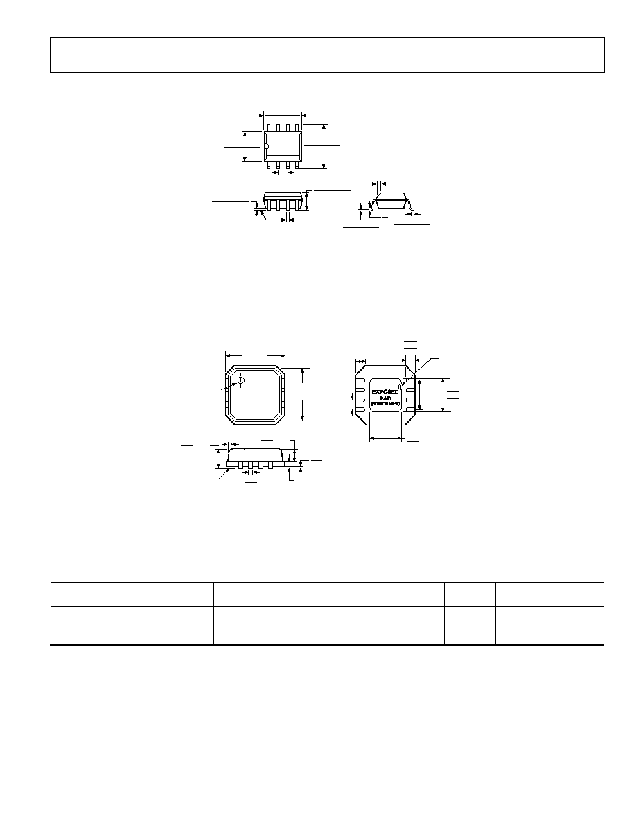
OUTLINE DIMENSIONS
0.25 (0.0098)
0.17 (0.0067)
1.27 (0.0500)
0.40 (0.0157)
0.50 (0.0196)
0.25 (0.0099)
◊
45∞
8∞
0∞
1.75 (0.0688)
1.35 (0.0532)
SEATING
PLANE
0.25 (0.0098)
0.10 (0.0040)
4
1
8
5
5.00 (0.1968)
4.80 (0.1890)
4.00 (0.1574)
3.80 (0.1497)
1.27 (0.0500)
BSC
6.20 (0.2440)
5.80 (0.2284)
0.51 (0.0201)
0.31 (0.0122)
COPLANARITY
0.10
CONTROLLING DIMENSIONS ARE IN MILLIMETERS; INCH DIMENSIONS
(IN PARENTHESES) ARE ROUNDED-OFF MILLIMETER EQUIVALENTS FOR
REFERENCE ONLY AND ARE NOT APPROPRIATE FOR USE IN DESIGN.
COMPLIANT TO JEDEC STANDARDS MS-012-AA
Figure 17. 8-Lead Standard Small Outline Package [SOIC_N]
Narrow Body
(R-8)
Dimensions shown in millimeters and (inches)
1
0.50
BSC
0.60 MAX
PIN 1
INDICATOR
1.50
REF
0.50
0.40
0.30
2.75
BSC SQ
TOP
VIEW
12∞ MAX
0.70 MAX
0.65 TYP
SEATING
PLANE
PIN 1
INDICATOR
0.90 MAX
0.85 NOM
0.30
0.23
0.18
0.05 MAX
0.01 NOM
0.20 REF
1.89
1.74
1.59
4
1.60
1.45
1.30
3.00
BSC SQ
5
8
Figure 18. 8-Lead Lead Frame Chip Scale Package [LFCSP_VD]
3 mm x 3 mm Body, Very Thin, Dual Lead
(CP-8-2)
Dimensions shown in millimeters
ORDERING GUIDE
Model
Temperature
Range
Package Description
Package
Option
Ordering
Quantity Branding
ADP3120AJRZ
1
0∞C to 85∞C
8-Lead Standard Small Outline Package (SOIC_N)
R-8
N/A
ADP3120AJRZ-RL
1
0∞C to 85∞C
8-Lead Standard Small Outline Package (SOIC_N)
R-8
2,500
ADP3120AJCPZ-RL
1
0∞C to 85∞C
8-Lead Lead Frame Chip Scale Package (LFCSP_VD)
CP-8-2
5,000
L3C
1
Z = Pb-free part.

ADP3120A
Rev. 0 | Page 14 of 16
NOTES

ADP3120A
Rev. 0 | Page 15 of 16
NOTES

ADP3120A
Rev. 0 | Page 16 of 16
NOTES
©2006 Analog Devices, Inc. All rights reserved. Trademarks and
registered trademarks are the property of their respective owners.
D05812-0-3/06(0)