 | –≠–ª–µ–∫—Ç—Ä–æ–Ω–Ω—ã–π –∫–æ–º–ø–æ–Ω–µ–Ω—Ç: ADP3181 | –°–∫–∞—á–∞—Ç—å:  PDF PDF  ZIP ZIP |
Document Outline
- FEATURES
- APPLICATIONS
- GENERAL DESCRIPTION
- FUNCTIONAL BLOCK DIAGRAM
- ˛ˇ
- ˛ˇ
- ˛ˇ
- ˛ˇ
- ˛ˇ
- ˛ˇ
- ˛ˇ
- ˛ˇ
- ˛ˇ
- ˛ˇ
- ˛ˇ
- ˛ˇ
- ˛ˇ
- ˛ˇ
- ˛ˇ
- ˛ˇ
- ˛ˇ
- ˛ˇ
- ˛ˇ
- ˛ˇ
- ˛ˇ
- ˛ˇ
- ˛ˇ
- ˛ˇ
- ˛ˇ
- ˛ˇ
- ˛ˇ
- ˛ˇ
- ˛ˇ
- ˛ˇ
- ˛ˇ
- ˛ˇ
- ˛ˇ
- ˛ˇ
- ˛ˇ
- ˛ˇ

5-Bit or 6-Bit Programmable 2-,3-,4-Phase
Synchronous Buck Controller
ADP3181
Rev. A
Information furnished by Analog Devices is believed to be accurate and reliable.
However, no responsibility is assumed by Analog Devices for its use, nor for any
infringements of patents or other rights of third parties that may result from its use.
Specifications subject to change without notice. No license is granted by implication
or otherwise under any patent or patent rights of Analog Devices. Trademarks and
registered trademarks are the property of their respective owners.
One Technology Way, P.O. Box 9106, Norwood, MA 02062-9106, U.S.A.
Tel: 781.329.4700
www.analog.com
Fax: 781.461.3113
©2005 Analog Devices, Inc. All rights reserved.
FEATURES
Selectable 2-, 3-, or 4-phase operation at up to 1 MHz per
phase
±14.5 mV worst-case mV differential sensing error over
temperature
Logic-level PWM outputs for interface to external high
power drivers
Active current balancing between all output phases
Built-in power good/crowbar blanking supports on-the-fly
VID code changes
Digitally programmable output can be switched between
VRM 9 (5-bit) and VRD 10 (6-bit) VID codes for
ADP3181JRU. (VRD10 (6-bit) only for ADP3181JRQ)
Programmable short circuit protection with programmable
latch-off delay
APPLICATIONS
Desktop PC power supplies for
next-generation Intel processors
VRM modules
FUNCTIONAL BLOCK DIAGRAM
19
11
12
15
10
28
13
14
26
8
25
24
23
17
18
22
21
20
16
1
2
3
4
5
7
6
9
27
VCC
GND
ADP3181
EN
DELAY
ILIMIT
PWRGD
RT
RAMPADJ
PWM2
FB
PWM3
PWM4
SW1
CSSUM
CSCOMP
SW2
SW3
SW4
CSREF
PWM1
VID4 VID3 VID2 VID1 VID0
FBRTN CPUID
COMP
PRECISION
REFERENCE
SOFT
START
UVLO
SHUTDOWN
AND BIAS
OSCILLATOR
VID
DAC
DAC + 300mV
DAC ≠ 250mV
CSREF
EN
CURRENT-
LIMITING
CIRCUIT
CURRENT-
BALANCING
CIRCUIT
DELAY
CROWBAR
CURRENT
LIMIT
CMP
CMP
CMP
CMP
2-/3-/4-PHASE
DRIVER LOGIC
EN
SET
RESET
RESET
RESET
RESET
04796-
0-
001
Figure 1.
GENERAL DESCRIPTION
The ADP3181 is a highly efficient multiphase synchronous
buck-switching regulator controller optimized for converting
a 12 V main supply into the core supply voltage required by
high performance Intel processors. It uses an internal 6-bit
DAC to read a voltage identification (VID) code directly from
the processor, which is used to set the output voltage. The
CPUID input selects whether the DAC codes match the
VRM 9 or VRD 10 specifications. It uses a multimode PWM
architecture to drive the logic-level outputs at a programmable
switching frequency that can be optimized for VR size and
efficiency. The phase relationship of the output signals can
be programmed to provide 2-, 3-, or 4-phase operation,
allowing for the construction of up to four complementary
buck-switching stages.
The ADP3181 also includes programmable no-load offset and
slope functions to adjust the output voltage as a function of the
load current so that it is always optimally positioned for a
system transient. The ADP3181 provides accurate and reliable
short-circuit protection, adjustable current limiting, and a
delayed power good output that accommodates on-the-fly
output voltage changes requested by the CPU.
The device is specified over the commercial temperature range
of 0∞C to +85∞C and is available in 28-lead QSOP (only VRD10
option) and TSSOP packages.

ADP3181
Rev. A | Page 2 of 24
TABLE OF CONTENTS
Specifications..................................................................................... 3
Test Circuits....................................................................................... 5
Absolute Maximum Ratings............................................................ 6
Pin Configuration and Function Descriptions............................. 7
Typical Performance Characteristics ............................................. 8
Theory of Operation ........................................................................ 9
Start-Up Sequence........................................................................ 9
Master Clock Frequency............................................................ 10
Output Voltage Differential Sensing ........................................ 10
Output Current Sensing ............................................................ 10
Active Impedance Control Mode............................................. 10
Current Control Mode and Thermal Balance ........................ 10
Voltage Control Mode................................................................ 11
Soft Start ...................................................................................... 12
Current Limit, Short Circuit, and Latch-Off Protection....... 12
Dynamic VID.............................................................................. 12
Power Good Monitoring ........................................................... 13
Output Crowbar ......................................................................... 13
Output Enable and UVLO ........................................................ 13
Applications..................................................................................... 15
Setting the Clock Frequency..................................................... 15
Soft Start and Current Limit Latch-Off Delay Times............ 15
Inductor Selection ...................................................................... 15
Designing an Inductor............................................................... 16
Output Droop Resistance.......................................................... 16
Inductor DCR Temperature Correction ................................. 17
Output Offset .............................................................................. 17
C
out
Selection ............................................................................... 17
Power MOSFETS........................................................................ 18
Ramp Resistor Selection............................................................ 19
Current Limit Setpoint .............................................................. 20
Feedback Loop Compensation Design.................................... 20
C
IN
Selection and Input Current DI/DT Reduction .............. 21
Building a Switchable VR9/VR10 Design ............................... 22
Layout and Component Placement.............................................. 23
General Recommendations....................................................... 23
Outline Dimensions ....................................................................... 24
Ordering Guide .......................................................................... 24
REVISION HISTORY
7/05--Rev. 0 to Rev. A
Added QSOP Package................................................................ 25
Change to Ordering Guide........................................................ 25
4/04--Revision 0: Initial Version

ADP3181
Rev. A | Page 3 of 24
SPECIFICATIONS
V
CC
= 12 V, FBRTN = GND, T
A
= 0∞C to +85∞C, unless otherwise noted.
1
Table 1.
Parameter Symbol
Conditions
Min
Typ
Max
Unit
ERROR AMPLIFIER
Output Voltage Range
2
V
COMP
0.7
3.1
V
Accuracy V
FB
Relative to nominal DAC output, referenced to
FBRTN, CSSUM = CSCOMP. See Figure 3.
-14.5
+14.5 mV
Line Regulation
V
FB
VCC = 10 V to 14 V.
0.05
%
Input Bias Current
I
FB
14
15.5
17
A
FBRTN Current
I
FBRTN
100
140
A
Output Current
I
O(ERR)
FB forced to V
OUT
- 3%.
500
A
Gain Bandwidth Product
GBW
(ERR)
COMP = FB.
20
MHz
Slew Rate
C
COMP
= 10 pF.
25
V/
s
VID INPUTS
Input Low Voltage
V
IL(VID)
CPUID > 4.5 V.
0.8
V
CPUID < 4.0 V.
0.4
V
Input High Voltage
V
IH(VID)
CPUID > 4.5 V.
2.0
V
CPUID < 4.0 V.
0.8
V
Input Current
I
VID
VID(X) = 0 V, CPUID > 4.5 V.
40
70
A
VID(X) = 0 V, CPUID < 4.0 V.
20
35
A
Pull-up Resistance
R
VID
40
60
k
Internal Pull-Up Voltage
CPUID > 4.5 V.
2.25
2.5
2.75
V
CPUID < 4.0 V.
1.1
1.25
1.4
V
VID Transition Delay Time
2
VID code change to FB change.
400
ns
No CPU Detection Turn-Off Delay Time
2
VID code change to 11111 to PWM going low.
400
ns
CPUID INPUT
Input Low Voltage
V
IL(CPUID)
0.4
V
Input High Voltage
V
IH(CPUID)
0.8
4.0
V
VR 9 Detection Threshold Voltage
4.0
4.5
V
Input Current
I
CPUID
CPUID = 0 V.
20
3.5
A
Pull-Up Resistance
R
CPUID
4.0
60
k
OSCILLATOR
Frequency Range
2
f
OSC
0.25
4
MHz
Frequency Variation
f
PHASE
T
A
= +25∞C, R
T
= 250 k
, 4-phase.
155 200
245 kHz
T
A
= +25∞C, R
T
= 115 k
, 4-phase.
400
kHz
T
A
= +25∞C, R
T
= 75 k
, 4-phase.
600
kHz
Output Voltage
V
RT
R
T
= 100 k
to GND.
1.9 2.0
2.1 V
RAMPADJ Output Voltage
V
RAMPADJ
RAMPADJ - FB.
-50
+50
mV
RAMPADJ Input Current Range
I
RAMPADJ
0
100
A
CURRENT SENSE AMPLIFIER
Offset Voltage
V
OS(CSA)
CSSUM - CSREF. See Figure 2. -3
+3
mV
Input Bias Current
I
BIAS(CSSUM)
-50
+50
nA
Gain Bandwidth Product
GBW
(CSA)
10
MHz
Slew Rate
C
CSCOMP
= 10 pF.
10
V/
s
Input Common Mode Range
CSSUM and CSREF.
0
2.7
V
Positioning Accuracy
V
FB
See Figure 4. -77
-80
-83
mV
Output Voltage Range
0.05
2.7
V
Output Current
I
CSCOMP
500
A

ADP3181
Rev. A | Page 4 of 24
Parameter Symbol
Conditions
Min
Typ
Max
Unit
CURRENT BALANCE CIRCUIT
Common Mode Range
V
SW(X)CM
-600
+200
mV
Input Resistance
R
SW(X)
SW(X) = 0 V.
20
30
40
k
Input Current
I
SW(X)
SW(X) = 0 V.
4
7
10
A
Input Current Matching
I
SW(X)
SW(X) = 0 V.
-5
+5
%
CURRENT
LIMIT
COMPARATOR
Output Voltage
Normal Mode
V
ILIMIT(NM)
EN > 0.8 V, R
ILIMIT
= 250 k
.
2.9 3 3.1 V
In Shutdown
V
ILIMIT(SD)
EN < 0.4 V, I
ILIMIT
= -100
A.
400
mV
Output Current, Normal Mode
I
ILIMIT(NM)
EN > 0.8 V, R
ILIMIT
= 250 k
.
12
A
Maximum Output Current
2
60
A
Current Limit Threshold Voltage
V
CL
V
CSREF
≠ V
CSCOMP
, R
ILIMIT
= 250 k
.
105 125 145 mV
Current Limit Setting Ratio
V
CL
/I
ILIMIT.
10.4
mV/
A
Delay Normal Mode Voltage
V
DELAY(NM)
R
DELAY
= 250 k
.
2.9 3 3.1 V
Delay Overcurrent Threshold
V
DELAY(OC)
R
DELAY
= 250 k
.
1.7 1.8 1.9 V
Latch-Off Delay Time
t
DELAY
R
DELAY
= 250 k
, C
DELAY
= 12 nF.
1.5
ms
SOFT
START
Output Current, Soft Start Mode
I
DELAY(SS)
During start-up, delay < 2.4 V.
15
20
25
A
Soft Start Delay Time
t
DELAY(SS)
R
DELAY
= 250 k
, C
DELAY
= 12 nF, VID code = 011111.
1
ms
ENABLE
INPUT
Input Low Voltage
V
IL(EN)
0.4
V
Input High Voltage
V
IH(EN)
0.8
V
Input Current, Input Voltage Low
I
IL(EN)
EN = 0 V.
-1
1
A
Input Current, Input Voltage High
I
IH(EN)
EN = 1.25 V.
10
25
A
POWER GOOD COMPARATOR
Undervoltage Threshold
V
PWRGD(UV)
Relative to nominal DAC output.
-180
-250
-320
mV
Overvoltage Threshold
V
PWRGD(OV)
Relative to nominal DAC output.
230
300
370
mV
Output Low Voltage
V
OL(PWRGD)
I
PWRGD(SINK)
= 4 mA.
225
400
mV
Power Good Delay Time
During Soft Start
2
R
DELAY
= 250 k
, C
DELAY
= 12 nF, VID code = 011111.
1 ms
VID Code Changing
100
250
s
VID Code Static
200
ns
Crowbar Trip Point
V
CROWBAR
Relative to nominal DAC output.
230
300
370
mV
Crowbar Reset Point
Relative to FBRTN.
630
700
770
mV
Crowbar Delay Time
t
CROWBAR
Overvoltage to PWM going low.
VID Code Changing
100
250
s
VID Code Static
400
ns
PWM
OUTPUTS
Output Low Voltage
V
OL(PWM)
I
PWM(SINK)
= -400
A.
160
500
mV
Output High Voltage
V
OH(PWM)
I
PWM(SOURCE)
= 400
A.
4.0 5
V
SUPPLY
DC Supply Current
5
10
mA
UVLO Threshold Voltage
V
UVLO
V
CC
rising.
6.5 6.9 7.3 V
UVLO
Hysteresis
0.7 0.9 1.1 V
1
All limits at temperature extremes are guaranteed via correlation using standard statistical quality control (SQC).
2
Guaranteed by design, not tested in production.

ADP3181
Rev. A | Page 5 of 24
TEST CIRCUITS
04796-0-005
CSSUM
18
CSCOMP
17
28
VCC
CSREF
16
GND
19
39k
100nF
1k
1.0V
ADP3181
12V
V
OS
=
CSCOMP≠1V
40
Figure 2. Current Sense Amplifier V
OS
12V
1.25V
100nF
ADP3181
1
2
3
28
27
26
4
8
10
12
14
5
6
7
21
24
23
22
9
11
17
18
19
13
15
16
20
25
5-BIT CODE
12nF
VID4
VID3
VID2
VID1
VID0
CPUID
FBRTN
FB
COMP
EN
PWRGD
DELAY
RT
RAMPADJ
VCC
PWM1
PWM2
PWM3
PWM4
SW1
SW2
SW3
SW4
CSCOMP
GND
CSSUM
CSREF
ILIMIT
1k
250k
20k
250k
100nF
1
F
+
04796-0-004
Figure 3. Closed-Loop Output Voltage Accuracy
04796-0-006
CSSUM
18
CSCOMP
17
28
VCC
CSREF
16
COMP
8
FB
9
GND
19
200k
10k
200k
1.0V
ADP3181
V
12V
V
FB
= FB
V = 80mV
≠ FB
V = 0mV
100nF
Figure 4. Positioning Voltage

ADP3181
Rev. A | Page 6 of 24
ABSOLUTE MAXIMUM RATINGS
Table 2.
Parameter
Rating
VCC
-0.3 V to 15 V
FBRTN
-0.3 V to +0.3 V
VID0 to VID4, CPUID, EN, DELAY, ILIMIT,
CSCOMP, RT, PWM1 to PWM4, COMP
-0.3 V to 5.5 V
SW1 to SW4
-5 V to +25 V
All Other Inputs and Outputs
-0.3 V to VCC +0.3 V
Storage Temperature
-65∞C to +150∞C
Operating Ambient Temperature
Range
0∞C to +85∞C
Operating Junction Temperature
125∞C
Thermal Impedance (
JA
)
100∞C/W
Lead Temperature
Soldering (10 sec)
300∞C
Infrared (15 sec)
260∞C
Stresses above those listed under Absolute Maximum Ratings
may cause permanent damage to the device. This is a stress
rating only and functional operation of the device at these or
any other conditions above those indicated in the operational
section of this specification is not implied. Exposure to absolute
maximum rating conditions for extended periods may affect
device reliability. Absolute maximum ratings apply individually
only, not in combination. Unless otherwise specified all other
voltages are referenced to GND.
ESD CAUTION
ESD (electrostatic discharge) sensitive device. Electrostatic charges as high as 4000 V readily accumulate on the
human body and test equipment and can discharge without detection. Although this product features
proprietary ESD protection circuitry, permanent damage may occur on devices subjected to high energy
electrostatic discharges. Therefore, proper ESD precautions are recommended to avoid performance
degradation or loss of functionality.
ADP3181
Rev. A | Page 7 of 24
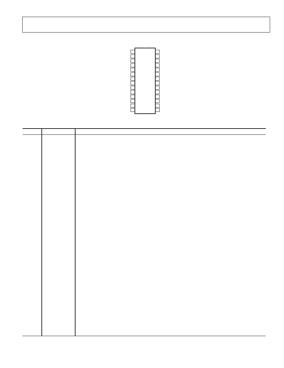
PIN CONFIGURATION AND FUNCTION DESCRIPTIONS
04796-0-011
ADP3181
TOP VIEW
(Not to Scale)
VID4
1
VCC
28
VID3
2
PWM1
27
VID2
3
PWM2
26
VID1
4
PWM3
25
VID0
5
PWM4
24
CPUID
6
SW1
23
FBRTN
7
SW2
22
FB
8
SW3
21
COMP
9
SW4
20
PWRGD
10
GND
19
EN
11
CSCOMP
18
DELAY
12
CSSUM
17
RT
13
CSREF
16
RAMPADJ
14
ILIMIT
15
Figure 5. Pin Configuration
Table 3. Pin Function Descriptions
Pin No.
Mnemonic
Description
1 to 5
VID4 to VID0
Voltage Identification DAC Inputs. These five pins are pulled up to an internal reference, providing a
Logic 1 if left open. When in normal operation mode, the DAC output programs the FB regulation voltage
based on the condition of the CPUID pin (see Table 4 and Table 5). Leaving VID4 through VID0 open results
in ADP3181 going into a no CPU mode, shutting off its PWM outputs.
6
CPUID
CPU DAC Code Selection Input. When this pin is pulled > 4.25 V, the internal DAC reads its inputs based on
the VRM 9 VID table (see Table 4). When this pin is <4 V, the DAC reads its inputs based on the VRD 10 VID
table (see Table 5) and treats CPUID as the VID5 input. (ADP3181JRQ, VRD10 only)
7
FBRTN
Feedback Return. VID DAC and error amplifier reference for remote sensing of the output voltage.
8
FB
Feedback Input. Error amplifier input for remote sensing of the output voltage. An external resistor
between this pin and the output voltage sets the no-load offset point.
9
COMP
Error Amplifier Output and Compensation Point.
10
PWRGD
Power Good Output. Open drain output that signals when the output voltage is outside of the proper
operating range.
11
EN
Power Supply Enable Input. Pulling this pin to GND disables the PWM outputs.
12
DELAY
Soft Start Delay and Current Limit Latch-off Delay Setting Input. An external resistor and capacitor
connected between this pin and GND sets the soft start ramp-up time and the overcurrent latch-off delay
time.
13
RT
Frequency Setting Resistor Input. An external resistor connected between this pin and GND sets the
oscillator frequency of the device.
14
RAMPADJ
PWM Ramp Current Input. An external resistor from the converter input voltage to this pin sets the internal
PWM ramp.
15
ILIMIT
Current Limit Set Point/Enable Output. An external resistor from this pin to GND sets the current limit
threshold of the converter. This pin is actively pulled low when the ADP3181 EN input is low, or when V
CC
is
below its UVLO threshold to signal to the driver IC that the driver high-side and low-side outputs should go
low.
16
CSREF
Current Sense Reference Voltage Input. The voltage on this pin is used as the reference for the current
sense amplifier and the power good and crowbar functions. This pin should be connected to the common
point of the output inductors.
17
CSSUM
Current Sense Summing Node. External resistors from each switch node to this pin sum the average
inductor currents together to measure the total output current.
18
CSCOMP
Current Sense Compensation Point. A resistor and capacitor from this pin to CSSUM determines the slope
of the load line and the positioning loop response time.
19
GND
Ground. All internal biasing and the logic output signals of the device are referenced to this ground.
20 to 23 SW4 to SW1
Current Balance Inputs. Inputs for measuring the current level in each phase. The SW pins of unused
phases should be left open.
24 to 27 PWM4 to PMW1 Logic-level PWM Outputs. Each output is connected to the input of an external MOSFET driver such as the
ADP3110. Connecting the PWM3 and/or PWM4 outputs to GND causes that phase to turn off, allowing the
ADP3181 to operate as a 2-, 3-, or 4-phase controller.
28
VCC
Supply Voltage for the Device.
ADP3181
Rev. A | Page 8 of 24
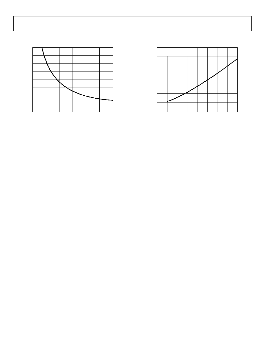
TYPICAL PERFORMANCE CHARACTERISTICS
4
3
2
1
0
0
50
100
150
200
250
300
04796-0-002
R
T
VALUE (k
)
MAS
T
E
R
CLOCK FRE
Q
UE
NCY
(MHz)
Figure 6. Master Clock Frequency vs. R
T
5.3
5.2
5.1
5.0
4.9
4.8
4.7
4.6
0
4.0
3.5
3.0
2.5
2.0
1.5
1.0
0.5
04796-0-003
OSCILLATOR FREQUENCY (MHz)
S
U
P
P
L
Y
CURRE
NT (mA)
T
A
= 25
∞
C
4-PHASE OPERATION
Figure 7. Supply Current vs. Oscillator Frequency

ADP3181
Rev. A | Page 9 of 24
THEORY OF OPERATION
The ADP3181 combines a multimode, fixed-frequency PWM
control with multiphase logic outputs for use in 2-, 3-, and
4-phase synchronous buck CPU core supply power converters.
The internal VID DAC can be used in Intel's 5-bit VRM 9 or
6-bit VRD/VRM 10 designs, depending on the setting of the
CPUID pin. Multiphase operation is important for producing
the high currents and low voltages demanded by today's micro-
processors. Handling the high currents in a single-phase
converter places high thermal demands on the components in
the system such as the inductors and MOSFETs. The multimode
control of the ADP3181 ensures a stable, high performance
topology for
∑ Balancing currents and thermals between phases.
∑ High speed response at the lowest possible switching
frequency and output decoupling.
∑ Minimizing thermal switching losses due to lower
frequency operation.
∑ Tight load line regulation and accuracy.
∑ High current output from 4-phase operational design.
∑ Reduced output ripple due to multiphase cancellation.
∑ PC board layout noise immunity.
∑ Ease of use and design due to independent component
selection.
∑ Flexibility in operation for tailoring design to low cost or
high performance.
START-UP SEQUENCE
Two functions are set during the start-up sequence: the number
of active phases and the VID DAC configuration. The number
of operational phases and their phase relationship is determined
by internal circuitry that monitors the PWM outputs. Normally,
the ADP3181 operates as a 4-phase PWM controller. Grounding
the PWM4 pin programs 3-phase operation and grounding the
PWM3 and PWM4 pins programs 2-phase operation.
When the ADP3181 is enabled, the controller outputs a voltage
on PWM3 and PWM4 that is approximately 675 mV. An
internal comparator checks each pin's voltage versus a threshold
of 300 mV. If the pin is grounded, then it is below the threshold
and the phase is disabled. The output resistance of the PWM
pin is approximately 5 k during this detection time. Any
external pull-down resistance connected to the PWM pin
should not be less than 25 k to ensure proper operation.
PWM1 and PWM2 are disabled during the phase detection
interval, which occurs during the first two clock cycles of the
internal oscillator. After this time, if the PWM output is not
grounded the 5 k resistance is removed and it switches
between 0 V and 5 V. If the PWM output is grounded then it
remains off.
The PWM outputs are logic-level devices intended for driving
external gate drivers such as the ADP3110. Because each phase
is monitored independently, operation approaching 100% duty
cycle is possible. Also, more than one output can be on at a time
for overlapping phases.
The VID DAC configuration is determined by the voltage pre-
sent at the CPUID pin. If this pin is pulled up to >4.5 V, the
VID DAC operates with five inputs and generates the VR 9
output voltage range, as shown in Table 4. If CPUID is <4 V, the
VID DAC treats CPUID as the VID5 input of VR 10 and
operates as a 6-bit DAC using the output voltage range given in
Table 5.
Table 4. VR 9 VID Codes for ADP3181JRU Only, CPUID >4.25
VID4
VID3
VID2
VID1
VID0
Output
1
1
1
1
1
No CPU
1
1
1
1
0
1.100 V
1
1
1
0
1
1.125 V
1
1
1
0
0
1.150 V
1
1
0
1
1
1.175 V
1
1
0
1
0
1.200 V
1
1
0
0
1
1.225 V
1
1
0
0
0
1.250 V
1
0
1
1
1
1.275 V
1
0
1
1
0
1.300 V
1
0
1
0
1
1.325 V
1
0
1
0
0
1.350 V
1
0
0
1
1
1.375 V
1
0
0
1
0
1.400 V
1
0
0
0
1
1.425 V
1
0
0
0
0
1.450 V
0
1
1
1
1
1.475 V
0
1
1
1
0
1.500 V
0
1
1
0
1
1.525 V
0
1
1
0
0
1.550 V
0
1
0
1
1
1.575 V
0
1
0
1
0
1.600 V
0
1
0
0
1
1.625 V
0
1
0
0
0
1.650 V
0
0
1
1
1
1.675 V
0
0
1
1
0
1.700 V
0
0
1
0
1
1.725 V
0
0
1
0
0
1.750 V
0
0
0
1
1
1.775 V
0
0
0
1
0
1.800 V
0 0 0 0 1 1.825
V
0 0 0 0 0 1.850
V

ADP3181
Rev. A | Page 10 of 24
MASTER CLOCK FREQUENCY
The clock frequency of the ADP3181 is set with an external
resistor connected from the RT pin to ground. The frequency
follows the graph in Figure 6. To determine the frequency per
phase, the clock is divided by the number of phases in use. If
PWM4 is grounded, then divide the master clock by 3 for the
frequency of the remaining phases. If PWM3 and 4 are
grounded, then divide by 2. If all phases are in use, divide by 4.
OUTPUT VOLTAGE DIFFERENTIAL SENSING
The ADP3181 combines differential sensing with a high
accuracy VID DAC and reference and a low offset error
amplifier to maintain a worst-case specification of ±14.5 mV
differential sensing error over its full operating output voltage
and temperature range. The output voltage is sensed between
the FB and FBRTN pins. FB should be connected through a
resistor to the regulation point, usually the remote sense pin of
the microprocessor. FBRTN should be connected directly to the
remote sense ground point. The internal VID DAC and
precision reference are referenced to FBRTN, which has a
minimal current of 100 A to allow accurate remote sensing.
The internal error amplifier compares the output of the DAC to
the FB pin to regulate the output voltage.
OUTPUT CURRENT SENSING
The ADP3181 provides a dedicated current sense amplifier
(CSA) to monitor the total output current for proper voltage
positioning versus load current and for current limit detection.
Sensing the load current at the output gives the total average
current being delivered to the load, which is an inherently more
accurate method then peak current detection or sampling the
current across a sense element such as the low side MOSFET.
This amplifier can be configured several ways depending on the
objectives of the system:
∑ Output inductor ESR sensing without a thermistor for
lowest cost.
∑ Output inductor ESR sensing with a thermistor for
improved accuracy with tracking of inductor temperature.
∑ Sense resistors for highest accuracy measurements.
The positive input of the CSA is connected to the CSREF pin,
which is connected to the output voltage. The inputs to the
amplifier are summed together through resistors from the
sensing element (such as the switch node side of the output
inductors) to the inverting input, CSSUM. The feedback resistor
between CSCOMP and CSSUM sets the gain of the amplifier,
and a filter capacitor is placed in parallel with this resistor. The
gain of the amplifier is programmable by adjusting the feedback
resistor to set the load line required by the microprocessor. The
current information is then given as the difference of CSREF ≠
CSCOMP. This difference signal is used internally to offset the
VID DAC for voltage positioning and as a differential input for
the current limit comparator.
To provide the best accuracy for the sensing of current, the CSA
has been designed to have a low offset input voltage. Also, the
sensing gain is determined by external resistors so that it can be
made extremely accurate.
ACTIVE IMPEDANCE CONTROL MODE
For controlling the dynamic output voltage droop as a function
of output current, a signal proportional to the total output cur-
rent at the CSCOMP pin can be scaled to be equal to the droop
impedance of the regulator times the output current. This
droop voltage is then used to set the input control voltage to the
system. The droop voltage is subtracted from the DAC refer-
ence input voltage directly to tell the error amplifier where the
output voltage should be. This differs from previous implemen-
tations and allows enhanced feed-forward response.
CURRENT CONTROL MODE AND THERMAL
BALANCE
The ADP3181 has individual inputs for each phase, which are
used for monitoring the current in each phase. This informa-
tion is combined with an internal ramp to create a current
balancing feedback system that has been optimized for initial
current balance accuracy and dynamic thermal balancing
during operation. This current balance information is indepen-
dent of the average output current information used for
positioning described previously.
The magnitude of the internal ramp can be set to optimize
the transient response of the system. It also monitors the supply
voltage for feed-forward control for changes in the supply.
A resistor connected from the power input voltage to the
RAMPADJ pin determines the slope of the internal PWM
ramp. Detailed information about programming the ramp is
given in the Applications section.
External resistors can be placed in series with individual phases
to create an intentional current imbalance, such as when one
phase may have better cooling and can support higher currents.
Resistors RSW1 through RSW4 (see the typical application cir-
cuit in Figure 10) can be used for adjusting thermal balance. It
is best to have the ability to add these resistors during the initial
design, so make sure placeholders are provided in the layout.
To increase the current in any phase, make R
SW
for that phase
larger (make R
SW
= 0 for the hottest phase; do not change
during balancing). Increasing R
SW
to only 500 makes a
substantial increase in phase current. Increase each R
SW
value by
small amounts to achieve balance, starting with the coolest
phase first.

ADP3181
Rev. A | Page 11 of 24
VOLTAGE CONTROL MODE
A high gain-bandwidth voltage mode error amplifier is used for
the voltage-mode control loop. The control input voltage to the
positive input is set via the VID logic. This voltage is also offset
by the droop voltage for active positioning of the output voltage
as a function of current, commonly known as active voltage
positioning. The output of the amplifier is the COMP pin,
which sets the termination voltage for the internal PWM ramps.
The negative input (FB) is tied to the output sense location with
a resistor RB and is used for sensing and controlling the output
voltage at this point. A current source from the FB pin flowing
through RB is used for setting the no-load offset voltage from
the VID voltage. The no-load voltage is negative with respect to
the VID DAC. The main loop compensation is incorporated in
the feedback network between FB and COMP.
Table 5. VR 10 VID Codes for the ADP3181, CPUID Used As a VID5 Input
VID4
VID3
VID2
VID1
VID0
CPUID
Output
VID4
VID3
VID2
VID1
VID0
CPUID
Output
1
1
1
1
1
1
No CPU
1
1
0
1
0
0
1.2125 V
1
1
1
1
1
0
No CPU
1
1
0
0
1
1
1.2250 V
0
1
0
1
0
0
0.8375 V
1
1
0
0
1
0
1.2375 V
0
1
0
0
1
1
0.8500 V
1
1
0
0
0
1
1.2500 V
0
1
0
0
1
0
0.8625 V
1
1
0
0
0
0
1.2625 V
0
1
0
0
0
1
0.8750 V
1
0
1
1
1
1
1.2750 V
0
1
0
0
0
0
0.8875 V
1
0
1
1
1
0
1.2875 V
0
0
1
1
1
1
0.9000 V
1
0
1
1
0
1
1.3000 V
0
0
1
1
1
0
0.9125 V
1
0
1
1
0
0
1.3125 V
0
0
1
1
0
1
0.9250 V
1
0
1
0
1
1
1.3250 V
0
0
1
1
0
0
0.9375 V
1
0
1
0
1
0
1.3375 V
0
0
1
0
1
1
0.9500 V
1
0
1
0
0
1
1.3500 V
0
0
1
0
1
0
0.9625 V
1
0
1
0
0
0
1.3625 V
0
0
1
0
0
1
0.9750 V
1
0
0
1
1
1
1.3750 V
0
0
1
0
0
0
0.9875 V
1
0
0
1
1
0
1.3875 V
0
0
0
1
1
1
1.0000 V
1
0
0
1
0
1
1.4000 V
0
0
0
1
1
0
1.0125 V
1
0
0
1
0
0
1.4125 V
0
0
0
1
0
1
1.0250 V
1
0
0
0
1
1
1.4250 V
0
0
0
1
0
0
1.0375 V
1
0
0
0
1
0
1.4375 V
0
0
0
0
1
1
1.0500 V
1
0
0
0
0
1
1.4500 V
0
0
0
0
1
0
1.0625 V
1
0
0
0
0
0
1.4625 V
0
0
0
0
0
1
1.0750 V
0
1
1
1
1
1
1.4750 V
0
0
0
0
0
0
1.0875 V
0
1
1
1
1
0
1.4875 V
1
1
1
1
0
1
1.1000 V
0
1
1
1
0
1
1.5000 V
1
1
1
1
0
0
1.1125 V
0
1
1
1
0
0
1.5125 V
1
1
1
0
1
1
1.1250 V
0
1
1
0
1
1
1.5250 V
1
1
1
0
1
0
1.1375 V
0
1
1
0
1
0
1.5375 V
1
1
1
0
0
1
1.1500 V
0
1
1
0
0
1
1.5500 V
1
1
1
0
0
0
1.1625 V
0
1
1
0
0
0
1.5625 V
1
1
0
1
1
1
1.1750 V
0
1
0
1
1
1
1.5750 V
1
1
0
1
1
0
1.1875 V
0
1
0
1
1
0
1.5875 V
1
1
0
1
0
1
1.2000 V
0
1
0
1
0
1
1.6000 V
ADP3181
Rev. A | Page 12 of 24
SOFT START
The power-on ramp up time of the output voltage is set with a
capacitor and resistor in parallel from the DELAY pin to
ground. The RC time constant also determines the current limit
latch-off time as explained in the following section. In UVLO or
when EN is a logic low, the DELAY pin is held at ground. After
the UVLO threshold is reached and EN is a logic high, the
DELAY capacitor is charged up with an internal 20 A current
source. The output voltage follows the ramping voltage on the
DELAY pin, limiting the inrush current. The soft start time
depends on the value of VID DAC and C
DLY
, with a secondary
effect from R
DLY
. Refer to the Applications section for detailed
information on setting C
DLY
.
If either EN is taken low or V
CC
drops below UVLO, the delay
capacitor is reset to ground to be ready for another soft start
cycle. Figure 8 shows the typical start-up waveforms for the
ADP3181.
Figure 8. Typical Start-up Waveforms, Channel 1: PWRGD, Channel 2: CSREF,
Channel 3: DELAY, Channel 4: COMP
CURRENT LIMIT, SHORT CIRCUIT, AND LATCH-OFF
PROTECTION
The ADP3181 compares a programmable current limit setpoint
to the voltage from the output of the current sense amplifier.
The level of current limit is set with the resistor from the
ILIMIT pin to ground. During normal operation, the voltage on
ILIMIT is 3 V. The current through the external resistor is inter-
nally scaled to give a current limit threshold of 10.4 mV/A. If
the difference in voltage between CSREF and CSCOMP rises
above the current limit threshold, the internal current limit
amplifier controls the internal COMP voltage to maintain the
average output current at the limit.
After the limit is reached, the 3 V pull-up on the DELAY pin is
disconnected, and the external DELAY capacitor is discharged
through the external resistor. A comparator monitors the
DELAY voltage and shuts off the controller when the voltage
drops below 1.8 V. The current limit latch-off delay time is thus
set by the RC time constant discharging from 3 V to 1.8 V. The
Applications section discusses the selection of C
DLY
and R
DLY
.
Since the controller continues to cycle the phases during the
latch-off delay time, the controller returns to normal operation
if the short is removed before the 1.8 V threshold is reached.
The recovery characteristic depends on the state of PWRGD. If
the output voltage is within the PWRGD window, the controller
resumes normal operation. However, if a short circuit has
caused the output voltage to drop below the PWRGD threshold,
then a soft start cycle is initiated.
The latch-off function can be reset by removing and reapplying
V
CC
to the ADP3181, or by pulling the EN pin low for a short
time. To disable the short circuit latch-off function, the external
resistor to ground should be left open and a high value (>1 M)
resistor should be connected from DELAY to VCC. This
prevents the DELAY capacitor from discharging so the 1.8 V
threshold is never reached. The resistor has an impact on the
soft start time because the current through it adds to the
internal 20 A current source.
Figure 9. Overcurrent Latch-off Waveforms. Channel 1: CSREF, Channel 2:
DELAY, Channel 3: COMP, Channel 4: Phase 1 Switch Node
During start-up when the output voltage is below 200 mV, a
secondary current limit is active because the voltage swing of
CSCOMP cannot go below ground. This secondary current
limit controls the internal COMP voltage to the PWM com-
parators to 2 V. This limits the voltage drop across the low-side
MOSFETs through the current balance circuitry. There is also
an inherent per phase current limit that protects individual
phases when one or more phases may stop functioning because
of a faulty component. This limit is based on the maximum
normal-mode COMP voltage.
DYNAMIC VID
The ADP3181 incorporates the ability to dynamically change
the VID input while the controller is running. This allows the
output voltage to change while the supply is running and sup-
plying current to the load. This is commonly referred to as
VID-on-the-fly (VID-OTF). A VID-OTF can occur under light
or heavy load conditions. The processor signals the controller
by changing the VID inputs in multiple steps from the start
code to the finish code. This change can be positive or negative.

ADP3181
Rev. A | Page 13 of 24
When a VID input changes state, the ADP3181 detects the
change and ignores the DAC inputs for a minimum of 400 ns.
This time is to prevent a false code due to logic skew while the
5 VID inputs are changing. Additionally, the first VID change
initiates the PWRGD and CROWBAR blanking functions for a
minimum of 250 s to prevent a false PWRGD or CROWBAR
event. Each VID change resets the internal timer.
POWER GOOD MONITORING
The power good comparator monitors the output voltage via
the CSREF pin. The PWRGD pin is an open drain output
whose high level (when connected to a pull-up resistor)
indicates that the output voltage is within the nominal limits
specified in the specifications above based on the VID voltage
setting. PWRGD goes low if the output voltage is outside of this
specified range, if all of the VID DAC inputs are high, or
whenever the EN pin is pulled low. PWRGD is blanked during a
VID-OTF event for a period of 250 s to prevent false signals
during the time the output is changing.
The PWRGD circuitry also incorporates an initial turn-on
delay time based on the delay ramp. The PWRGD pin is held
low until the DELAY pin has reached 2.8 V. The time between
when the PWRGD undervoltage threshold is reached and when
the DELAY pin reaches 2.8 V provides the turn-on delay time.
This time is incorporated into the soft start ramp. To ensure a 1
ms delay time on PWRGD, the soft start ramp must also be >1
ms. Refer to the Applications section for detailed information
on setting C
DLY
.
OUTPUT CROWBAR
As part of the protection for the load and output components of
the supply, the PWM outputs are driven low (turning on the
low-side MOSFETs) when the output voltage exceeds the upper
crowbar threshold. This crowbar action stops once the output
voltage has fallen below the release threshold of about 700 mV.
Turning on the low-side MOSFETs pulls down the output as the
reverse current builds up in the inductors. If the output
overvoltage is due to a short of the high-side MOSFET, this
action current limits the input supply or blows its fuse,
protecting the microprocessor from destruction.
OUTPUT ENABLE AND UVLO
The VCC to the controller must be higher than the UVLO
threshold and the EN pin must be higher then its logic
threshold for the ADP3181 to begin switching. IF UVLO is less
than the threshold or the EN pin is a logic low, the device is
disabled. This holds the PWM outputs at ground, shorts the
DELAY capacitor to ground, and holds the ILIMIT pin at
ground.
In the application circuit, the ILIMIT pin should be connected
to the OD pins of the ADP3110 drivers. Because ILIMIT is
grounded, this disables the drivers such that both DRVH and
DRVL are grounded. This feature is important to prevent dis-
charging of the output capacitors when the controller is shut off.
If the driver outputs were not disabled, then a negative voltage
could be generated on the output due to the high current dis-
charge of the output capacitors through the inductors.
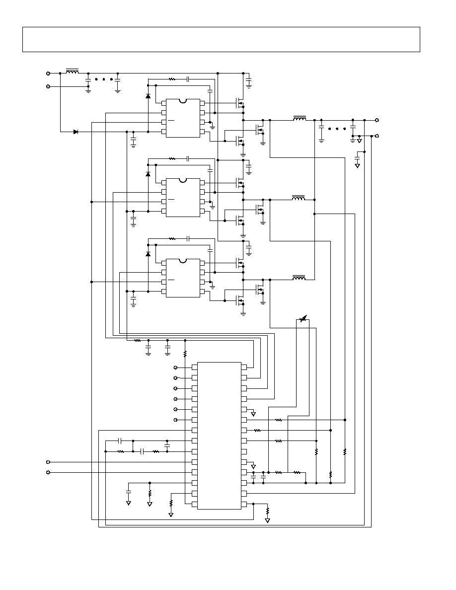
ADP3181
04796-0-008
Rev. A | Page 14 of 24
V
IN
12V
V
IN
RTN
ENABLE
POWER
GOOD
R
LIM
200k
R
PH1
124k
FROM CPU
R
R
383k
Q2
IPD06N03L
Q5
IPD06N03L
Q8
IPD06N03L
Q1
IPD12N03L
Q3
IPD06N03L
Q4
IPD12N03L
C
DLY
12nF
V
CC(CORE)
0.8375V ≠ 1.6V
65A AVG, 74A PK
V
CC(CORE) RTN
L2
600nH/1.6m
L1
1.6
H
C1
C6
R
T
249k
C12
10nF
C21
C28
L3
600nH/1.6m
C11
4.7
F
D2
1N4148WS
D3
1N4148WS
D4
1N4148WS
C8
10nF
C7
4.7
F
C9
4.7
F
C13
4.7
F
C17
4.7
F
U2
ADP3110
U3
ADP3110
U4
ADP3110
3
1
4
5
26
25
24
2
28
27
6
10
14
7
8
9
19
22
21
20
23
11
12
13
15
18
17
16
U1
ADP3181
Q7
IPD12N03L
C16
10nF
L4
600nH/1.6m
C15
4.7
F
R4
10
R
A
16.9k
C
FB
33pF
C
A
390pF
C
CS1
2.2nF
C
CS2
1.5nF
470
F/16V
◊
6
NICHICON PW SERIES
820
F/2.5V
◊
8
FUJITSU RE SERIES
8m
ESR (EACH)
10
F
◊
23
MLCC
IN
SOCKET
RTH
100k
, 5%
D1
1N4148WS
R
B
1.33k
R
CS1
35.7k
C
B
1.5nF
R
PH3
124k
R
DLY
330k
Q9
IPD06N03L
Q6
IPD06N03L
R
SW1
*
R
SW3
*
R
SW2
*
R
CS2
73.2k
R
PH2
124k
1
2
3
8
7
6
4
5
BST
IN
OD
VCC
DRVH
SW
PGND
DRVL
1
2
3
8
7
6
4
5
BST
IN
OD
VCC
DRVH
SW
PGND
DRVL
1
2
3
8
7
6
4
5
BST
IN
OD
VCC
DRVH
SW
PGND
DRVL
VID4
VID3
VID2
VID1
VID0
CPUID
FBRTN
FB
COMP
EN
PWRGD
DELAY
RT
RAMPADJ
VCC
PWM1
PWM2
PWM3
PWM4
SW1
SW2
SW3
SW4
CSCOMP
GND
CSSUM
CSREF
ILIMIT
+
+
C19
1
F
C20
33
F
+
+
+
*FOR A DESCRIPTION OF
OPTIONAL R
SW
RESISTORS,
SEE THE THEORY OF
OPERATION SECTION.
R1
2.2
C10
18nF
R2
2.2
C14
18nF
R3
2.2
C18
18nF
Figure 10. Typical VR 10 Application Circuit

ADP3181
Rev. A | Page 15 of 24
APPLICATIONS
The design parameters for a typical ADP3181 CPU application
are as follows:
∑ Input voltage (V
IN
) = 12 V
∑ VID setting voltage (V
VID
) = 1.500 V
∑ Duty cycle (D) = 0.125
∑ Nominal output voltage at no load (V
ONL
) = 1.480 V
∑ Nominal output voltage at 65 A load (
VOFL
) = 1.3825 V
∑ Static output voltage drop based on a 1.5 m load line (R
O
)
from no load to full load:
(V) = V
ONL
- V
OFL
V = 1.480 V - 1.3825 V = 97.5 mV
∑ Maximum output current (I
O
) = 65 A
∑ Number of phases (n) = 3
∑ Switching frequency per phase (f
SW
) = 330 kHz
SETTING THE CLOCK FREQUENCY
The ADP3181 uses a fixed-frequency control architecture. The
frequency is set by an external timing resistor (R
T
). The clock
frequency and the number of phases determine the switching
frequency per phase, which relates directly to switching losses
and the sizes of the inductors and input and output capacitors.
With n = 3 for three phases, a clock frequency of 990 kHz sets
the switching frequency of each phase, f
SW
, to 330 kHz, which
represents a practical trade-off between the switching losses and
the sizes of the output filter components. Figure 6 shows that to
achieve a 990 kHz oscillator frequency, the correct value for R
T
is 200 k. For good initial accuracy and frequency stability, it is
recommended to use a 1% resistor.
SOFT START AND CURRENT LIMIT LATCH-OFF
DELAY TIMES
Because the soft start, PWRGD delay, and current limit latch-
off delay functions all share the DELAY pin, these three
parameters must be considered together. The first step is to set
C
DLY
for the PWRGD delay ramp. This ramp is generated by a
20 A internal current source. The value of R
DLY
has a second-
order impact on the soft start time because it sinks part of the
current source to ground. However, as long as R
DLY
is greater
than 200 k, this effect is minor. The value for C
DLY
can be
approximated using
)
(
)
(
V
8
.
2
2
V
8
.
2
A
20
UV
PWRGD
VID
PWRGD
DLY
UV
PWRGD
VID
DLY
V
V
t
R
V
V
C
-
-
◊
◊
-
-
-
=
(1)
where t
PWRGD
is the desired PWRGD delay time and V
PWRGD(UV)
is
the undervoltage threshold for the PWRGD comparator.
Assuming an R
DLY
of 250 k and a desired PWRGD delay time
of 1 s, C
DLY
is 12 nF. The soft start delay time can then be
calculated using
DLY
VID
VID
DLY
ss
R
V
V
C
t
◊
-
◊
=
2
A
20
(2)
Once C
DLY
has been chosen, R
DLY
can be calculated for the
current limit latch-off time using
DLY
DELAY
DLY
C
t
R
◊
=
2
(3)
If the result for R
DLY
is less than 200 k, then a smaller soft start
time should be considered by recalculating the equation for
C
DLY
or a longer latch-off time should be used. In no case should
R
DLY
be less than 200 k. In this example, a delay time of 2 ms
gives R
DLY
= 333 k. The closest standard 5% value is 330 k.
Substituting 330 k back into Equations 1 and 2 shows that the
PWRGD delay and soft start times do not change significantly.
INDUCTOR SELECTION
The choice of inductance for the inductor determines the ripple
current in the inductor. Less inductance leads to more ripple
current, which increases the output ripple voltage and conduc-
tion losses in the MOSFETs, but allows using smaller size
inductors and, for a specified peak-to-peak transient deviation,
less total output capacitance. Conversely, a higher inductance
means lower ripple current and reduced conduction losses, but
requires larger size inductors and more output capacitance for
the same peak-to-peak transient deviation. In any multiphase
converter, a practical value for the peak-to-peak inductor ripple
current is less than 80% of the maximum DC current in the
same inductor. Equation 3 shows the relationship between the
inductance, oscillator frequency, and peak-to-peak ripple
current in the inductor. Equation 4 determines the minimum
inductance based on a given output ripple voltage:
L
f
D
V
I
SW
VID
RIPPLE
◊
-
=
)
1
(
(4)
(
)
(
(
)
)
RIPPLE
SW
O
VID
V
f
D
n
D
R
V
L
◊
◊
-
◊
-
◊
◊
=
1
1
(5)
Intel recommends that the ripple voltage should not exceed
10 mV peak-to-peak at the socket. Solving Equation 4 for a 12
mV peak-to-peak output ripple voltage at the regulator's output
to allow for drops through the PCB traces yields
(
)
nH
310
mV
12
kHz
330
375
.
0
1
875
.
0
m
5
.
1
V
5
.
1
=
◊
-
◊
◊
◊
L
(6)

ADP3181
Rev. A | Page 16 of 24
If the ripple voltage is less than that designed for, the inductor
can be made smaller until the ripple value is met. This allows
optimal transient response and minimum output decoupling.
The smallest possible inductor should be used to minimize the
number of output capacitors. A 300 nH inductor is a good
choice to start, and it gives a calculated ripple current of 13.3 A,
which is 61% of the full load current of 21.7 A. The inductor
should not saturate at the peak current of 29 A, and should be
able to handle the sum of the power dissipation caused by the
average current of 22 A in the winding and the core loss.
Another important factor in the inductor design is the DCR,
which is used for measuring the phase currents. A large DCR
causes excessive power losses, while too small a value leads to
increased measurement error. A good rule is to have the DCR
be about 1 to 1Ω times the droop resistance or DC output
resistance (R
O
).
DESIGNING AN INDUCTOR
Once the inductance and DCR are known, the next step is to
design an inductor or find a standard inductor that comes as
close as possible to meeting the overall design goals. It is also
important to have the inductance and DCR tolerance specified
to keep the accuracy of the system controlled. Using 15% for the
inductance and 8% for the DCR (at room temperature) are
reasonable tolerances that most manufacturers can meet.
The first decision in designing the inductor is to choose the
core material. There are several possibilities for providing low
core loss at high frequencies. Two examples are the powder
cores (Kool-MÆ from Magnetics, Inc., or Micrometals) and
the gapped soft ferrite cores (3F3 or 3F4 from Philips). Low
frequency powdered iron cores should be avoided due to their
high core loss, especially when the inductor value is relatively
low and the ripple current is high.
The best choice for a core geometry are closed-loop types, such
as pot cores, PQ, U, and E cores, or toroids. A good compromise
between price and performance are cores with a toroidal shape.
There are many useful references for quickly designing a power
inductor, such as
∑ Magnetic Designer Software Intusoft
(http://www.intusoft.com)
∑ Designing Magnetic Components for High Frequency
DC-DC Converters, McLyman, Kg Magnetics,
ISBN 1-883107-00-08
Selecting a Standard Inductor
The following power inductor manufacturers can provide design
consultation and deliver power inductors optimized for high
power applications upon request:
∑ Coilcraft
(847) 639-6400
www.coilcraft.com
∑ Coiltronics
(561) 752-5000
www.coiltronics.com
∑ Sumida Corporation
(510) 668-0660
www.sumida.com
∑ Vishay
(402) 563-6866
www.vishay.com
OUTPUT DROOP RESISTANCE
The design requires that the regulator output voltage measured
at the CPU pins drops when the output current increases. The
specified voltage drop corresponds to R
O
.
The output current is measured by summing together the
voltage across each inductor and then passing the signal
through a low-pass filter. This summer filter is the CS amplifier
configured with resistors R
PH(X)
(summers), and R
CS
and C
CS
(filter). The output resistance of the regulator is set by these
equations, where R
L
is the DCR of the output inductors:
L
X
PH
CS
O
R
R
R
R
◊
=
)
(
(7)
CS
L
CS
R
R
L
C
◊
=
(8)
One has the flexibility of choosing either R
CS
or R
PH(X).
It is best
to start with R
PH(X)
in the range of 100 k to 200 k, then solve
for R
CS
by rearranging Equation 7. Using 100 k for R
PH(X)
k
8
.
93
k
100
m
6
.
1
m
5
.
1
)
(
=
◊
=
◊
=
CS
X
PH
L
O
CS
R
R
R
R
R
Next, use equation 8 to solve for C
CS
:
nF
0
.
2
k
8
.
93
m
6
.
1
nH
300
=
◊
=
CS
C
The closest standard value for C
CS
is 1.8 nF. If the calculated
value does not happen to be a standard value, then recalculate
for the closest 1% resistor values for R
CS
and R
PH(X)
using the
final selected value for C
CS
. This can be quickly calculated by
multiplying the original values of R
CS
and R
PH(X)
by the ratio of
the calculated C
CS
to the actual value used. For best accuracy,
C
CS
should be a 5% or 10% NPO capacitor. For this example, the
actual values used for R
CS
and R
PH(X)
are 104.2 k and 111.1 k.
The closest standard 1% value for R
PH(X)
is 110 k. R
CS
is used
later and should not be rounded yet.

ADP3181
Rev. A | Page 17 of 24
INDUCTOR DCR TEMPERATURE CORRECTION
With the inductor's DCR being used as the sense element, and
copper wire being the source of the DCR, it is necessary to
compensate for temperature changes of the inductor's winding.
Fortunately, copper has a well-known temperature coefficient
(TC) of 0.39%/∞C.
If R
CS
is designed to have an opposite and equal percentage
change in resistance to that of the wire, it cancels the temp-
erature variation of the inductor's DCR. Due to the nonlinear
nature of NTC thermistors, resistors R
CS1
and R
CS2
are needed
(see Figure 11) to linearize the NTC and produce the desired
temperature tracking.
04796-0-009
CSSUM
18
CSCOMP
PLACE AS CLOSE AS POSSIBLE
TO NEAREST INDUCTOR
OR LOW-SIDE MOSFET
17
CSREF
16
ADP3181
C
CS
1.8nF
R
CS1
R
TH
R
CS2
KEEP THIS PATH
AS SHORT AS POSSIBLE
AND WELL AWAY FROM
SWITCH NODE LINES
TO
SWITCH
NODES
TO
V
OUT
SENSE
R
PH1
R
PH3
R
PH2
Figure 11. Temperature Compensation Circuit Values
The following procedure yields values to use for R
CS1
, R
CS2
, and
R
TH
(the thermistor value at 25∞C) for a given R
CS
value.
1. Select an NTC to be used based on type and value. Because
there is no value yet, start with a thermistor with a value
close to R
CS
. The NTC should also have an initial tolerance
of better than 5%.
2. Based on the type of NTC, find its relative resistance value
at two temperatures. Temperatures that work well are 50∞C
and 90∞C. We call these resistance values A (A is R
TH
(50∞C)/
R
TH
(25∞C)) and B (B is R
TH
(90∞C)/R
TH
(25∞C)). The NTC's
relative value is always 1 at 25∞C.
3. Find the relative value of R
CS
required for each of these
temperatures. This is based on the percentage change
needed, which can be 0.39%/∞C, initially. These are r
1
(r
1
is
1/(1+ TC ◊ (T1 - 25))) and r
2
(r
2
is 1/(1 + TC ◊ (T2 - 25)))
where TC = 0.0039, T1 = 50∞C, and T2 = 90∞C.
4. Compute the relative values for R
CS1
, R
CS2
, and R
TH
:
(
)
(
)
(
)
(
)
(
)
(
)
B
A
r
A
B
r
B
A
r
A
B
r
B
A
r
r
B
A
R
2
1
1
2
2
1
CS2
-
-
◊
-
◊
-
◊
-
◊
◊
-
◊
+
◊
-
◊
-
◊
◊
-
=
1
1
1
1
(9)
(
)
CS2
1
CS2
CS1
r
r
A
r
A
R
-
-
-
-
=
1
1
1
CS1
CS2
TH
r
r
R
1
1
1
1
-
-
=
Calculate R
TH
= r
TH
◊ R
CS
, then select the closest value of
thermistor available. Also compute a scaling factor k based on
the ratio of the actual thermistor value used relative to the
computed one:
(
)
(
)
CALCULATED
TH
ACTUAL
TH
R
R
k =
(10)
Calculate values for R
CS1
and R
CS2
using the following:
CS1
CS
CS1
r
k
R
R
◊
◊
=
(11)
))
(
)
1
((
CS2
CS
CS2
r
k
k
R
R
◊
+
-
◊
=
For this example, R
CS
has already been calculated in the
previous section to be 104.2 k, so start with a thermistor value
of 100 k. Looking through available 0603 size thermistors,
find a Vishay NTHS0603N01N1003JR NTC thermistor with
A = 0.3602 and B = 0.09174. From these values compute
r
CS1
= 0.3796, r
CS2
= 0.7195, and r
TH
= 1.0751. Solving for R
TH
yields 112.05 k, so choose 100 k, making k = 0.8925. Finally,
find R
CS1
and R
CS2
to be 35.30 k and 78.11 k. Choosing the
closest 1% resistor values yields 35.7 k and 78.7 k.
OUTPUT OFFSET
Intel's specification requires that at no load the nominal output
voltage of the regulator be offset to a lower value than the
nominal voltage corresponding to the VID code. The offset is
set by a constant current source flowing out of the FB pin (I
FB
)
and flowing through R
B
. The value of R
B
B
B
can be found using
Equation 12. The closest standard 1% resistor value is 1.33 k.
FB
ONL
VID
B
I
V
V
R
-
=
(12)
k
33
.
1
A
15
V
480
.
1
V
5
.
1
=
-
=
B
R
C
OUT
SELECTION
The required output decoupling for the regulator is typically
recommended by Intel for various processors and platforms.
Using some simple design guidelines determines what is
required. These guidelines are based on having both bulk and
ceramic capacitors in the system.
First, select the total amount of ceramic capacitance based on
the number and type of capacitor to be used. The best location
for ceramics is inside the socket, with 12 to 18 of size 1,206
being the physical limit. Others can be also placed along the
outer edge of the socket.

ADP3181
Rev. A | Page 18 of 24
Combined ceramic values of 200 F to 300 F made up of
multiple 10 F or 22 F capacitors are recommended. Select the
number of ceramics and find the total ceramic capacitance (C
Z
).
Next, there is an upper limit imposed on the total amount of
bulk capacitance (C
X
) when considering the VID-OTF voltage
stepping of the output (voltage step V
V
in time t
V
) and a lower
limit based on meeting the critical capacitance for load release
for a given maximum load step I
MAX
:
-
◊
◊
◊
Z
VID
O
STEP
MIN
X
C
V
R
n
I
L
C
)
(
(13)
(
)
MAX
X
C
Z
O
V
VID
v
VID
V
O
C
L
nKR
V
V
t
V
V
R
nK
L
-
-
◊
+
◊
◊
1
1
2
2
2
=
V
ERR
V
V
n
K 1
where
(14)
where R
X
is the ESR of the bulk capacitor bank. To meet the
transient specification, R
X
cannot be greater than 3 ◊ R
O
.
If the C
X(MIN)
is larger than C
X(MAX)
, the system does not meet the
VID-OTF specification and may require the use of a smaller
inductor or more phases (the switching frequency may need to
be increased to keep the output ripple the same).
This example uses twelve 22 F 1206 MLC capacitors
(CZ=264 F). The VID on-the-fly step change is 12.5 mV in
5 s. Solving for the bulk capacitance, assuming that R
X
= R
O
,
and where k = 4.6, yields
(
)
mF
92
.
5
F
230
V
5
.
1
m
3
.
1
3
A
60
nH
600
=
-
◊
◊
◊
MIN
X
C
(
)
◊
◊
◊
◊
◊
V
5
.
1
m
3
.
1
6
.
4
3
mV
250
nH
600
2
2
MAX
X
C
mF
9
.
23
F
230
1
nH
320
mV
450
m
3
1.
4.6
3
V
5
1.
s
150
1
2
=
-
-
◊
◊
◊
◊
◊
+
Using ten 560 F OSCONs with an ESR of 12 m each yields
C
X
= 5.6 mF with an R
X
= 1.2 m (making the new limits on C
X
2.4 mF to 8.8 mF, which is still within the acceptable range).
One last check should be made to ensure that the ESL of the
bulk capacitors (L
X
) is low enough to limit the initial high
frequency transient spike. This can be tested using
pH
89
3
m
3
.
1
F
230
2
=
◊
◊
X
2
O
Z
X
L
R
C
L
(15)
In this example, L
X
is 400 pH for the 10 OSCSON capacitors,
which satisfies this limitation. If the L
X
of the chosen bulk
capacitor bank is too large, the number of MLC capacitors must
be increased.
Note that for this multimode control technique, all ceramic
designs can be used as long as the conditions of Equations 11,
12, and 13 are satisfied.
POWER MOSFETS
For this example, the N channel power MOSFETs have been
selected for one high-side switch and two low-side switches per
phase. The main selection parameters for the power MOSFETs
are V
GS(TH)
, Q
G
, C
ISS
, C
RSS
, and R
DS(ON)
. The minimum gate drive
voltage (the supply voltage to the ADP3110) dictates whether
standard threshold or logic-level threshold MOSFETs must be
used. With V
GATE
~10 V, logic-level threshold MOSFETs
(V
GS(TH)
< 2.5 V) are recommended.
The maximum output current I
O
determines the R
DS(ON)
requirement for the low-side (synchronous) MOSFETs. In the
ADP3181, currents are balanced between phases, so the current
in each low-side MOSFET is the output current divided by the
total number of MOSFETs (n
SF
). With conduction losses being
dominant, the following expression shows the total power being
dissipated in each synchronous MOSFET in terms of the ripple
current per phase (I
R
) and average total output current (I
O
).
(
)
( )
SF
DS
SF
R
SF
O
SF
R
n
I
n
n
I
D
P
◊
◊
◊
+
◊
-
=
2
2
12
1
1
(16)
Knowing the maximum output current being designed for and
the maximum allowed power dissipation, the required R
DS(ON)
for the MOSFET can be found. For D pak MOSFETs up to an
ambient temperature of 50∞C, a safe limit for P
SF
is 1 W
(assuming 2 D paks) at 120∞C junction temperature. Thus, for
this example (65 A maximum), R
DS(SF)
(per MOSFET) < 8.7 mW.
This R
DS(SF)
is also at a junction temperature of about 120∞C, so
it is important to account for this when making this selection.
Another important factor for the synchronous MOSFET is the
input capacitance and feedback capacitance. The ratio of the
feedback to input needs to be small (less than 10% is recom-
mended) to prevent accidentally turning on the synchronous
MOSFETs when the switch node goes high.
Also, the time to switch the synchronous MOSFETs off should
not exceed the nonoverlap dead time of the MOSFET driver
(40 ns typical for the ADP3110). The output impedance of the
driver is about 2 and the typical MOSFET input gate resis-
tances are about 1 to 2 , so a total gate capacitance of less
than 6,000 pF should be adhered to. Since there are two

ADP3181
Rev. A | Page 19 of 24
MOSFETs in parallel, limit the input capacitance for each
synchronous MOSFET to 3,000 pF.
The high-side (main) MOSFET must be able to handle two
main power dissipation components; conduction and switching
losses. The switching loss is related to the amount of time it
takes for the main MOSFET to turn on and off, and to the
current and voltage that are being switched. Basing the
switching speed on the rise and fall time of the gate driver
impedance and MOSFET input capacitance, the following
expression provides an approximate value for the switching loss
per main MOSFET, where nMF is the total number of main
MOSFETs:
(
)
ISS
MF
O
MF
O
CC
SW
MF
S
C
n
n
R
n
I
V
f
P
◊
◊
◊
◊
◊
◊
= 2
(17)
Here, R
G
is the total gate resistance (2 for the ADP3110 and
about 1 for typical high speed switching MOSFETs, making
R
G
= 3 ) and C
ISS
is the input capacitance of the main
MOSFET. It is interesting to note that adding more main
MOSFETs (n
MF
) does not improve the switching loss per
MOSFET because the additional gate capacitance slows down
switching. The best method to reduce switching loss is to use
lower gate capacitance devices.
The conduction loss of the main MOSFET is given by the
following, where R
DS(MF)
is the on-resistance of the MOSFET:
(
)
(
)
MF
DS
MF
R
MF
O
MF
C
R
n
I
n
n
I
D
P
◊
◊
◊
+
◊
=
2
2
12
1
(18)
Typically, for main MOSFETs, the highest speed (low C
ISS
)
device is desirable, but these usually have higher on-resistance.
A device that meets the total power dissipation (about 1.5 W for
a single D pak) when combining the switching and conduction
losses should be selected.
For this example, an Infineon IPD12N03L was selected as the
main MOSFET (three total; n
MF
= 3), with a C
ISS
= 1460 pF
(max) and R
DS(MF)
= 14 m (max at T
J
= 120∫C), and an
Infineon IPD06N03L was selected as the synchronous MOSFET
(six total; n
SF
= 6), with C
ISS
= 2,370 pF (max), and R
DS(SF)
= 8.3
m (max at T
J
= 120∞C). The synchronous MOSFET C
ISS
is less
than 3,000∞pF, satisfying that requirement. Solving for the
power dissipation per MOSFET at I
O
= 65 A and I
R
= 13 A
yields 900 mW for each synchronous MOSFET and 1.6 W for
each main MOSFET. These numbers work well considering
there is usually more PCB area available for each main
MOSFET versus each synchronous MOSFET.
One last thing to consider is the power dissipation in the driver
for each phase. This is best described in terms of the Q
G
for the
MOSFETs and is given by the following, where Q
GMF
is the total
gate charge for each main MOSFET and Q
GSF
is the total gate
charge for each synchronous MOSFET:
(
)
CC
CC
GSF
SF
GMF
MF
SW
DRV
V
I
Q
n
Q
n
n
f
P
◊
+
◊
+
◊
◊
◊
=
2
(19)
Also shown is the standby dissipation factor (I
CC
◊ V
CC
) for the
driver. For the ADP3110, the maximum dissipation should be
less than 400 mW. For our example, with I
CC
= 7 mA, Q
GMF
=
22.8 nC and Q
GSF
= 34.3 nC, there is 260 mW in each driver,
which is below the 400 mW dissipation limit.
RAMP RESISTOR SELECTION
The ramp resistor (R
R
) is used for setting the size of the internal
PWM ramp. The value of this resistor is chosen to provide the
best combination of thermal balance, stability, and transient
response. The following expression is used for determining the
optimum value:
k
81
3
pF
5
m
2
.
4
5
3
nH
0
60
0.2
3
=
◊
◊
◊
◊
=
◊
◊
◊
◊
=
R
R
DS
D
R
R
R
C
R
A
L
A
R
(20)
where
A
R
is the internal ramp amplifier gain
A
D
is the current balancing amplifier gain
R
DS
is the total low-side MOSFET on-resistance
C
R
is the internal ramp capacitor value
The closest standard 1% resistor value is 226 k.
The internal ramp voltage magnitude can be calculated using
(
)
(
)
V
m
51
.
0
kHz
267
pF
5
k
83
3
V
5
1.
125
0.
1
0.2
1
=
◊
◊
◊
-
◊
=
◊
◊
◊
-
◊
=
R
SW
R
R
VID
R
R
V
f
C
R
V
D
A
V
(21)
The size of the internal ramp can be made larger or smaller.
If it is made larger, stability and transient response improve,
but thermal balance degrades. Likewise, if the ramp is made
smaller, thermal balance improves at the sacrifice of transient
response and stability. The factor of three in the denominator of
equation 20 sets a ramp size that gives an optimal balance for
good stability, transient response, and thermal balance.

ADP3181
Rev. A | Page 20 of 24
CURRENT LIMIT SETPOINT
To select the current limit setpoint, we need to find the resistor
value for R
LIM
. The current limit threshold for the ADP3181
is set with a 3 V source (V
LIM
) across R
LIM
with a gain of
10 mV/A (A
LIM
). R
LIM
can be found using the following:
O
LIM
LIM
LIM
LIM
R
I
V
A
R
◊
◊
=
(22)
Here, I
LIM
is the average current limit for the output of the
supply. For our example, using 90 A for I
LIM
, we find R
LIM
to be
222.2 k, for which we chose 221 k as the nearest 1% value.
The per phase current limit described earlier has its limit
determined by the following:
(
)
(
)
2
R
MAX
DS
D
BIAS
R
MAX
COMP
PHLIM
I
R
A
V
V
V
I
+
◊
-
-
(23)
For the ADP3181, the maximum COMP voltage (V
COMP(MAX)
)
is 3.3 V, the COMP pin bias voltage (V
BIAS
) is 1.2 V, and the
current balancing amplifier gain (A
D
) is 5. Using a V
R
of 0.7 V
and a R
DS(MAX)
of 5.3 m (low-side on-resistance at 150∞C), the
per-phase limit is 52 A.
This limit can be adjusted by changing the ramp voltage, V
R
.
Make sure not to set the per-phase limit lower than the average
per-phase current (I
LIM/n
).
FEEDBACK LOOP COMPENSATION DESIGN
Optimized compensation of the ADP3181 allows the best pos-
sible response of the regulator's output to a load change. The
basis for determining the optimum compensation is to make
the regulator and output decoupling appear as an output impe-
dance that is entirely resistive over the widest possible fre-
quency range, including DC, and equal to the droop resistance
(R
O
). With the resistive output impedance, the output voltage
droops in proportion with the load current at any load current
slew rate; this ensures the optimal positioning and allows the
minimization of the output decoupling.
With the multimode feedback structure of the ADP3181, one
needs to set the feedback compensation to make the converter's
output impedance working in parallel with the output decoup-
ling meet this goal. There are several poles and zeros created by
the output inductor and decoupling capacitors (output filter)
that need to be compensated for.
A type three compensator on the voltage feedback is adequate
for proper compensation of the output filter. The expressions
given below are intended to yield an optimal starting point for
the design; some minor adjustments may be necessary to
account for PCB and component parasitic effects.
Using Equations 24 to 28, compute the time constants for all of
the poles and zeros in the system, where, for the ADP3181, R is
the PCB resistance from the bulk capacitors to the ceramics and
R
DS
is approximately the total low-side MOSFET on-resistance
per phase at 25∞C. For this example, A
D
is 5, V
R
equals 1 V, R¥ is
approximately 0.6 m (assuming a 4-layer motherboard), and
L
X
is 400 pH for the 10 OSCSON capacitors.
(
)
VID
O
X
RT
VID
RT
L
DS
D
O
E
V
R
C
n
V
D
n
L
V
V
R
R
A
R
n
R
◊
◊
◊
◊
◊
-
◊
◊
+
◊
+
◊
+
◊
=
1
2
(24)
(
)
m
9
.
37
V
5
1.
m
3
1.
mF
56
.
6
3
V
63
0.
375
0.
1
nH
600
2
V
5
1.
V
63
0.
m
6
1.
m
2
.
4
5
m
3
1.
3
=
◊
◊
◊
◊
-
◊
◊
+
◊
+
◊
+
◊
=
E
R
(
)
(
)
s
79
.
4
m
0
1.
m
0.6
m
3
1.
m
3
1.
pH
75
3
m
6
0.
m
3
1.
mF
56
.
6
'
'
=
-
◊
+
-
◊
=
-
◊
+
-
◊
=
X
O
O
X
O
X
A
R
R
R
R
L
R
R
C
T
(25)
(
)
(
)
ns
97
.
1
mF
56
.
6
m
3
1.
m
6
0.
m
0
.
1
'
=
◊
-
+
=
◊
-
+
=
X
O
X
B
C
R
R
R
T
(26)
s
2
.
6
m
9
.
37
V
5
1.
kHz
267
2
m
2
.
4
5
nH
600
V
63
0.
2
=
◊
◊
◊
-
◊
=
◊
◊
◊
-
◊
=
E
VID
SW
DS
D
RT
C
R
V
f
R
A
L
V
T
(27)
(
)
(
)
ns
521
m
3
1.
F
230
m
6
0.
m
3
1.
mF
56
.
6
m
3
.
1
F
230
mF
56
.
6
'
2
2
=
◊
+
-
◊
◊
◊
=
◊
+
-
◊
◊
◊
=
O
Z
O
X
O
Z
X
D
R
C
R
R
C
R
C
C
T
(28)
The compensation values can be solved using the following:

ADP3181
Rev. A | Page 21 of 24
pF
371
k
33
1.
m
79
.
3
s
79
.
4
m
3
1.
3
=
◊
◊
◊
=
◊
◊
◊
=
A
B
E
A
O
A
C
R
R
T
R
n
C
(29)
k
.7
6
1
pF
71
3
s
2
.
6
=
=
=
A
C
A
C
T
R
(30)
nF
48
.
1
k
33
1.
s
97
.
1
=
=
=
B
B
B
R
T
C
(31)
pF
2
.
31
k
.7
6
1
ns
521
=
=
=
A
D
FB
R
T
C
(32)
Choosing the closest standard values for these components
yields C
A
= 820 pF, R
A
= 7.87 k, C
B
= 1.2 nF, and CFB = 100 pF.
These make a good starting point.
Using the design spreadsheet yields more optimal compen-
sation values; from the spreadsheet, C
A
= 680 pF, R
A
= 5.49 k,
C
B
= 1.2 nF, and C
C
IN
SELECTION AND INPUT CURRENT DI/DT
REDUCTION
In continuous inductor-current mode, the source current of the
high-side MOSFET is approximately a square wave with a duty
ratio equal to n ◊ V
OUT
/V
IN
and an amplitude of one-nth of the
maximum output current. To prevent large voltage transients, a
low ESR input capacitor sized for the maximum rms current
must be used. The maximum rms capacitor current is given by
A
5
.
10
1
125
0.
3
1
A
65
125
.
0
1
=
-
◊
◊
◊
=
◊
◊
◊
=
CRMS
O
CRMS
I
D
N
I
D
I
(33)
Note that the capacitor manufacturer's ripple current ratings are
often based on only 2,000 hours of life. This makes it advisable
to further derate the capacitor, or to choose a capacitor rated at
a higher temperature than required. Several capacitors may be
placed in parallel to meet size or height requirements in the
design. In this example, the input capacitor bank is formed by
three 2,200 F, 16 V Nichicon capacitors with a ripple current
rating of 3.5 A each.
B
FB
= 68 pF.
To reduce the input-current di/dt to below the recommended
maximum of 0.1 A/s, an additional small inductor (L > 1 H @
15 A) should be inserted between the converter and the supply
bus. That inductor also acts as a filter between the converter
and the primary power source.
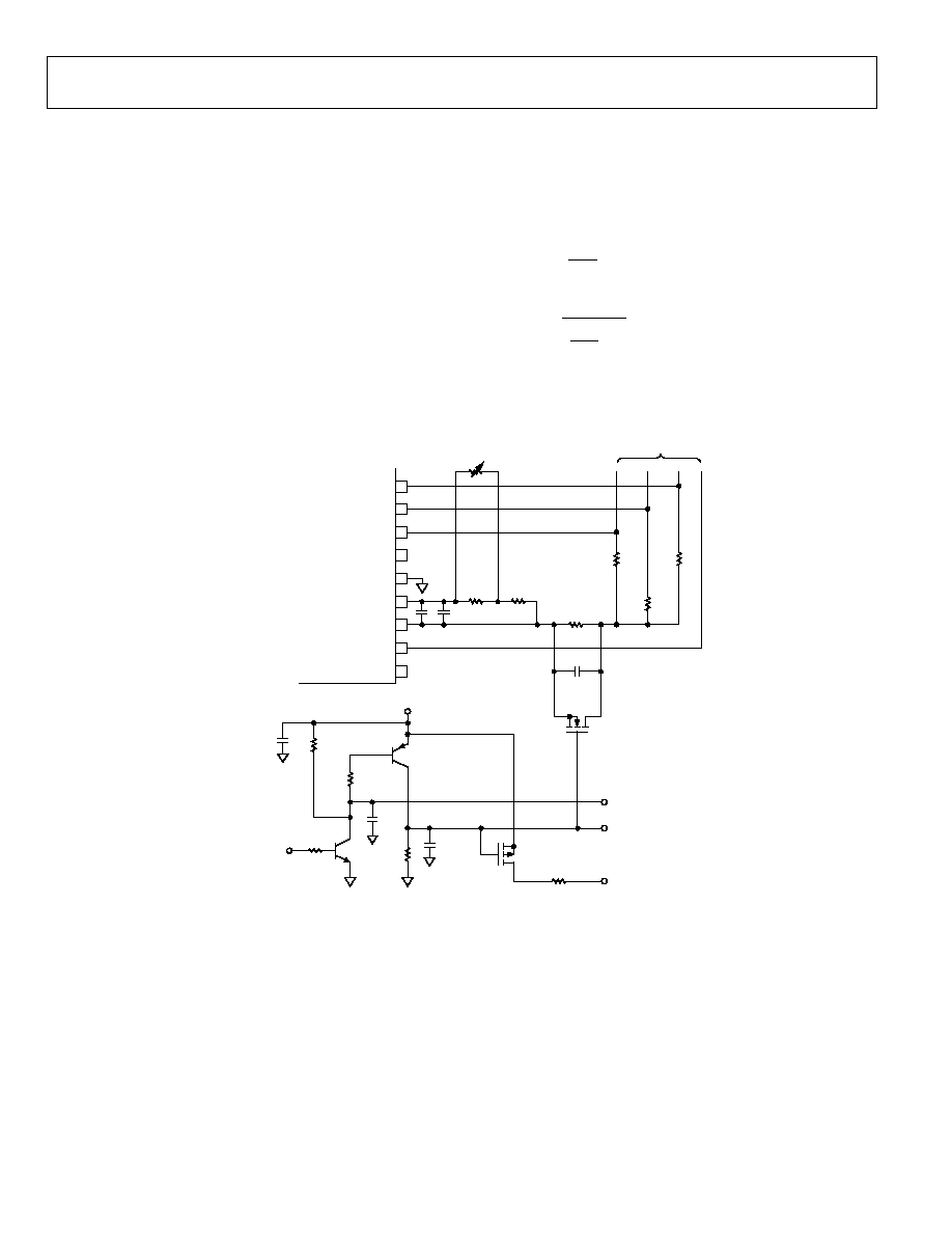
ADP3181
Rev. A | Page 22 of 24
BUILDING A SWITCHABLE VR9/VR10 DESIGN
Some designs may require the ability to work with either a VR9-
or a VR10-based CPU, because both processors are available in
the same package/pin count. To accomplish this, the voltage
regulator must detect which processor is present and set the
VID DAC and load line accordingly. This can be accomplished
using the BOOTSELECT output from the CPU. Figure 12
shows how this signal is used to modify the load line and set the
CPUID pin of the ADP3181 appropriately.
To determine the values of x and y, start with the two load lines,
R
OL
(smaller slope) and R
OH
(larger slope). First, follow the
standard design procedure, which gives the values for R
CS1
, R
CS2
,
and C
CS
for R
OL
. Tune R
PH
and C
CS
. Next, compute the values for
R
CS3
and C
CS3
using the following:
CS
OL
OH
CS
R
R
R
R
◊
-
=
1
3
(34)
-
=
1
3
OL
OH
CS
CS
R
R
C
C
(35)
In this case, R
OL
is 1.5 m and R
OH
is 3 m.
04796-0-010
R
PH1
124k
19
15
18
17
16
23
22
21
20
ADP3181
5VSB
TO
PHASE INDUCTORS
C
CS1
2.2nF
C
CS2
1.5nF
R
CS1
35.7k
R
PH3
124k
10k
10k
2.7k
2N3905
BSS84
2N3904
2N7001
R
CS2
73.2k
R
CS3
C
CS3
51
R
PH2
124k
RTH
100k
, 5%
BOOTSELECT
CPU NWD HI
CPU PSC HI
TO APD3181
CPUID (PIN 6)
100nF
100nF
100nF
10k
SW1
SW2
SW3
SW4
GND
CSCOMP
CSSUM
CSREF
ILIMIT
Figure 12. Connections to Allow Automatic Switching between VR9 and VR10 Operation

ADP3181
Rev. A | Page 23 of 24
LAYOUT AND COMPONENT PLACEMENT
The following guidelines are recommended for optimal
performance of a switching regulator in a PC system.
GENERAL RECOMMENDATIONS
For good results, at least a 4-layer PCB is recommended.
This should allow the needed versatility for control circuitry
interconnections with optimal placement, power planes for
ground, input, and output power, and wide interconnection
traces in the rest of the power delivery current paths. Keep in
mind that each square unit of 1 oz copper trace has a resistance
of ~0.53 mW at room temperature.
Whenever high currents must be routed between PCB layers,
use vias liberally to create several parallel current paths so that
the resistance and inductance introduced by these current paths
are minimized and the via current rating is not exceeded.
If critical signal lines (including the output voltage sense lines of
the ADP3181) must cross through power circuitry, it is best if a
signal ground plane can be interposed between those signal
lines and the traces of the power circuitry. This serves as a
shield to minimize noise injection into the signals at the
expense of making signal ground a bit noisier.
An analog ground plane should be used around and under the
ADP3181 for referencing the components associated with the
controller. This plane should be tied to the nearest output
decoupling capacitor ground and should not tie to any other
power circuitry to prevent power currents from flowing in it.
The components around the ADP3181 should be located close
to the controller with short traces. The most important traces to
keep short and away from other traces are the FB and CSSUM
pins. See Figure 6 for details on layout for the CSSUM node.
The output capacitors should be connected as closely as possible
to the load (or connector) that receives the power (for example,
a microprocessor core). If the load is distributed, the capacitors
should also be distributed and generally in proportion to where
the load is more dynamic.
Avoid crossing any signal lines over the switching power path
loop as described in the following section.
Power Circuitry
The switching power path should be routed on the PCB to
encompass the shortest possible length to minimize radiated
switching noise energy (EMI) and conduction losses in the
board. Failure to take proper precautions often results in EMI
problems for the entire PC system and noise-related operational
problems in the power converter control circuitry. The switch-
ing power path is the loop formed by the current path through
the input capacitors and the power MOSFETs, including all
interconnecting PCB traces and planes. The use of short and
wide interconnection traces is especially critical in this path
because it minimizes the inductance in the switching loop,
which can cause high energy ringing. These traces also accom-
modate the high current demand with minimal voltage loss.
Whenever a power-dissipating component (for example, a
power MOSFET) is soldered to a PCB, the liberal use of vias,
both directly on the mounting pad and immediately sur-
rounding it, is recommended. Two important reasons for this
are improved current rating through the vias and improved
thermal performance from vias extended to the opposite side of
the PCB where a plane can more readily transfer the heat to the
air. Make a mirror image of any pad being used to heat sink the
MOSFETs on the opposite side of the PCB to achieve the best
thermal dissipation to the air around the board. To further
improve thermal performance, use the largest possible pad area.
The output power path should also be routed to encompass a
short distance. The output power path is formed by the current
path through the inductor, the output capacitors, and the load.
For best EMI containment, a solid power ground plane should
be used as one of the inner layers extending fully under all the
power components.
Signal Circuitry
The output voltage is sensed and regulated between the FB pin
and the FBRTN pin (which connects to the signal ground at the
load). In order to avoid differential mode noise pickup in the
sensed signal, the loop area should be small. Thus the FB and
FBRTN traces should be routed adjacent to each other atop the
power ground plane back to the controller.
Connect the feedback traces from the switch nodes as close as
possible to the inductor. The CSREF signal should be connected
to the output voltage at the nearest inductor to the controller.
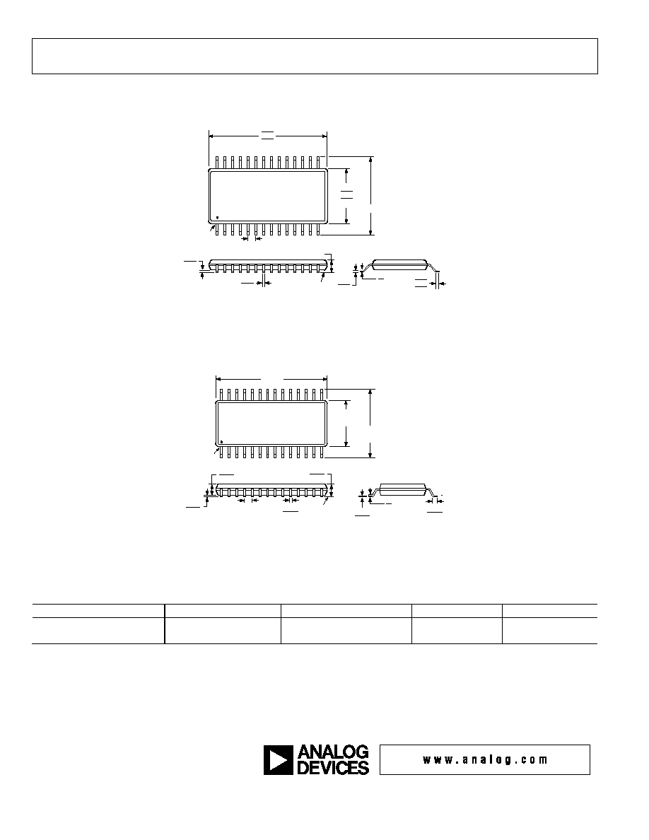
ADP3181
Rev. A | Page 24 of 24
OUTLINE DIMENSIONS
COMPLIANT TO JEDEC STANDARDS MO-153-AE
2 8
1 5
1 4
1
8 ∞
0 ∞
SEATING
PLANE
COPLANARITY
0.10
1.20 MAX
6.40 BSC
0.65
BSC
PIN 1
0.30
0.19
0.20
0.09
4.50
4.40
4.30
0.75
0.60
0.45
9.80
9.70
9.60
0.15
0.05
Figure 13. 28-Lead Thin Shrink Small Outline Package [TSSOP]
(RU-28)
Dimensions shown in millimeters
28
15
14
1
PIN 1
SEATING
PLANE
8∞
0∞
0.236
BSC
0.154
BSC
0.012
0.008
0.025
BSC
0.010
0.004
COPLANARITY
0.004
0.065
0.049
0.069
0.053
0.010
0.006
0.050
0.016
0.390
BSC
COMPLIANT TO JEDEC STANDARDS MO-137-AF
Figure 14. 28-Lead Shrink Small Outline Package [QSOP]
(RQ-28)
Dimensions shown in inches
ORDERING GUIDE
Part Number
Temperature Package
Package Description
Package Outline
Quantity per Reel
ADP3181JRUZ-REEL
1
0∞C to +85∞C
TSSOP--13" Reel
RU-28
2500
ADP3181JRQZ-RL
1, 2
0∞C to +85∞C
QSOP--13" Reel
RQ-28
2500
1
Z = PB-free part.
2
VRD10 only.
©2005 Analog Devices, Inc. All rights reserved. Trademarks and
registered trademarks are the property of their respective owners.
D04796
≠
0≠7/05(A)