 | –≠–ª–µ–∫—Ç—Ä–æ–Ω–Ω—ã–π –∫–æ–º–ø–æ–Ω–µ–Ω—Ç: ADP3182 | –°–∫–∞—á–∞—Ç—å:  PDF PDF  ZIP ZIP |
Adjustable Output 1-/2-/3-Phase
Synchronous Buck Controller
ADP3182
Rev. 0
Information furnished by Analog Devices is believed to be accurate and reliable.
However, no responsibility is assumed by Analog Devices for its use, nor for any
infringements of patents or other rights of third parties that may result from its use.
Specifications subject to change without notice. No license is granted by implication
or otherwise under any patent or patent rights of Analog Devices. Trademarks and
registered trademarks are the property of their respective owners.
One Technology Way, P.O. Box 9106, Norwood, MA 02062-9106, U.S.A.
Tel: 781.329.4700
www.analog.com
Fax: 781.326.8703
© 2004 Analog Devices, Inc. All rights reserved.
FEATURES
Selectable 1-, 2-, or 3-phase operation at up to 1 MHz per
phase
±2% worst-case differential sensing error over temperature
Externally adjustable 0.8 V to >5 V output from a 12 V supply
Logic-level PWM outputs for interface to external high
power drivers
Active current balancing between all output phases
Built-in power good/crowbar functions
Programmable short-circuit protection with programmable
latch-off delay
APPLICATIONS
Auxiliary supplies
DDR memory supplies
Point-of-load modules
GENERAL DESCRIPTION
The ADP3182 is a highly efficient multiphase, synchronous,
buck-switching regulator controller optimized for converting a
12 V main supply into a high current, low voltage supply for use
in point-of-load (POL) applications. It uses a multimode PWM
architecture to drive the logic-level outputs at a programmable
switching frequency that can be optimized for VR size and
efficiency. The phase relationship of the output signals can be
programmed to provide 1-, 2-, or 3-phase operation, allowing
for the construction of up to three complementary buck-
switching stages. The ADP3182 also provides accurate and
reliable short-circuit protection and adjustable current limiting.
ADP3182 is specified over the commercial temperature range of
0∞C to +85∞C and is available in a 20-lead QSOP package.
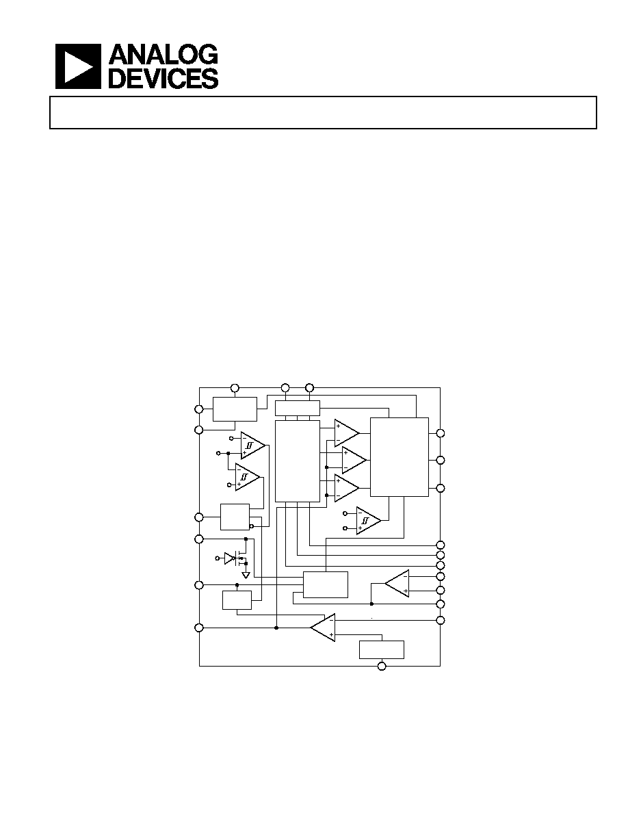
FUNCTIONAL BLOCK DIAGRAM
04938-001
VCC
800mV
REFERENCE
SOFT
START
DELAY
UVLO
SHUTDOWN
& BIAS
OSCILLATOR
GND
ADP3182
14
EN
6
DELAY
7
ILIMIT
10
PWRGD
5
1
RT
8
RAMPADJ
9
PWM2
19
3
FB
PWM3
18
SW1
17
CSSUM
12
CSCOMP
13
SW2
16
SW3
15
CSREF
11
PWM1
FBRTN
2
COMP
4
950mV
1.05V
650mV
FB
FB
EN
CURRENT
LIMIT
CIRCUIT
CROWBAR
CURRENT
LIMIT
CURRENT
BALANCING
CIRCUIT
2 / 3-PHASE
DRIVER LOGIC
EN
SET
RESET
RESET
RESET
20
CMP
CMP
CMP
Figure 1.

ADP3182
Rev. 0 | Page 2 of 20
TABLE OF CONTENTS
Specifications..................................................................................... 3
Test Circuits....................................................................................... 5
Absolute Maximum Ratings............................................................ 6
ESD Caution.................................................................................. 6
Pin Configuration and Function Description .............................. 7
Typical Performance Characteristics ............................................. 8
Theory of Operation ........................................................................ 9
Start-Up Sequence........................................................................ 9
Master Clock Frequency.............................................................. 9
Output Voltage Differential Sensing .......................................... 9
Output Current Sensing .............................................................. 9
Current Control Mode and Thermal Balance ........................ 10
Voltage Control Mode................................................................ 10
Soft Start ...................................................................................... 10
Current Limit, Short-Circuit, and Latch-off Protection ....... 10
Power Good Monitoring ........................................................... 11
Output Crowbar ......................................................................... 11
Output Enable and UVLO ........................................................ 12
Applications..................................................................................... 14
Setting the Clock Frequency..................................................... 14
Soft Start and Current Limit Latch-Off Delay Time ............. 14
Inductor Selection ...................................................................... 14
Output Current Sense................................................................ 15
Output Voltage............................................................................ 16
Power MOSFETs......................................................................... 16
Ramp Resistor Selection............................................................ 17
Current Limit Setpoint .............................................................. 17
Feedback Loop Compensation Design.................................... 17
Input Capacitor Selection and Input Current di/dt ............... 18
Inductor DCR Temperature Correction ................................. 18
Layout and Component Placement ......................................... 19
Outline Dimensions ....................................................................... 20
Ordering Guide .......................................................................... 20
REVISION HISTORY
10/04--Revision 0: Initial Version

ADP3182
Rev. 0 | Page 3 of 20
SPECIFICATIONS
VCC = 12 V, FBRTN = GND, T
A
= 0∞C to 85∞C, unless otherwise noted.
1
Table 1.
Parameter Symbol
Conditions
Min
Typ
Max
Unit
OSCILLATOR
Frequency Range
2
f
OSC
0.25
3
MHz
Frequency Variation
f
PHASE
T
A
= 25∞C, R
T
= 348 k
, 3-phase
155 200 245 kHz
T
A
= 25∞C, R
T
= 174 k
, 3-phase
400
kHz
T
A
= 25∞C, R
T
= 100 k
, 3-phase
600
kHz
Output Voltage
V
RT
R
T
= 100 k
to GND
1.9 2.0 2.1 V
RAMPADJ Output Voltage
V
RAMPADJ
RAMPADJ - FB
-50
+50
mV
RAMPADJ Input Current Range
I
RAMPADJ
0
100
µA
VOLTAGE ERROR AMPLIFIER
Output Voltage Range
2
V
COMP
0.7
3.1
V
Accuracy V
FB
Referenced to FBRTN
784
800
816
mV
Line Regulation
V
FB
VCC = 10 V to 14 V
0.05
%
Input Bias Current
I
FB
FB = 800 mV
-4
+4
µA
FBRTN Current
I
FBRTN
100
140
µA
Output Current
I
O(ERR)
FB forced to V
OUT
- 3%
500
µA
Gain Bandwidth Product
GBW
(ERR)
COMP = FB
20
MHz
Slew Rate
C
COMP
= 10 pF
25
V/
µs
CURRENT SENSE AMPLIFIER
Offset Voltage
V
OS(CSA)
CSSUM - CSREF, Figure 2
-5.5
+5.5
mV
Input Bias Current
I
BIAS(CSSUM)
-50
+50
nA
Gain Bandwidth Product
GBW
(CSA)
10
MHz
Slew Rate
C
CSCOMP
= 10 pF
10
V/
µs
Input Common-Mode Range
CSSUM and CSREF
0
VCC - 2.5
V
Output Voltage Range
0.05
VCC - 2.5
V
Output Current
I
CSCOMP
500
µA
CURRENT BALANCE CIRCUIT
Common-Mode Range
V
SW(X)CM
-600
+200
mV
Input Resistance
R
SW(X)
SW(X) = 0 V
20
30
40
k
Input Current
I
SW(X)
SW(X) = 0 V
4
7
10
µA
Input Current Matching
I
SW(X)
SW(X) = 0 V
-7
+7
%
CURRENT LIMIT COMPARATOR
Output Voltage
Normal
Mode
V
ILIMIT(NM)
EN > 2 V, R
ILIMIT
= 250 k
2.9 3 3.1 V
In Shutdown Mode
V
ILIMIT(SD)
EN < 0.8 V, I
ILIMIT
= -100
µA
400
mV
Output Current, Normal Mode
I
ILIMIT(NM)
EN > 2 V, R
ILIMIT
= 250 k
12
µA
Maximum Output Current
2
60
µA
Current Limit Threshold Voltage
V
CL
V
CSREF
- V
CSCOMP
, R
ILIMIT
= 250 k
105 125 145 mV
Current Limit Setting Ratio
V
CL
/I
ILIMIT
10.4
mV/
µA
DELAY Normal Mode Voltage
V
DELAY(NM)
R
DELAY
= 250 k
2.9 3 3.1 V
DELAY Overcurrent Threshold
V
DELAY(OC)
R
DELAY
= 250 k
1.7 1.8 1.9 V
Latch-Off Delay Time
t
DELAY
R
DELAY
= 250 k
, C
DELAY
= 12 nF
1.5
ms
SOFT START
Output Current, Soft Start Mode
I
DELAY(SS)
During start-up, DELAY < 2.4 V
15
20
25
µA
Soft Start Delay Time
t
DELAY(SS)
R
DELAY
= 250 k
, C
DELAY
= 12 nF
500
µs
ADP3182
Rev. 0 | Page 4 of 20
Parameter Symbol
Conditions
Min
Typ
Max
Unit
ENABLE INPUT
Input Low Voltage
V
IL(EN)
0.8
V
Input High Voltage
V
IH(EN)
2.0
V
Input Current
I
IN(EN)
-1
+1
µA
POWER GOOD COMPARATOR
Undervoltage Threshold
V
PWRGD(UV)
Relative to FBRTN
600
660
720
mV
Overvoltage Threshold
V
PWRGD(OV)
Relative to FBRTN
880
940
1000
mV
Output Low Voltage
V
OL(PWRGD)
I
PWRGD(SINK)
= 4 mA
225
400
mV
Power Good Delay Time
200
ns
Crowbar Trip Point
V
CROWBAR
Relative to FBRTN
0.975
1.05
1.1
V
Crowbar Reset Point
Relative to FBRTN
550
650
750
mV
Crowbar Delay Time
t
CROWBAR
Overvoltage to PWM going low
400
ns
PWM OUTPUTS
Output Low Voltage
V
OL(PWM)
I
PWM(SINK)
= -400
µA
160
500
mV
Output High Voltage
V
OH(PWM)
I
PWM(SOURCE)
= 400
µA
4.0 5
V
SUPPLY
DC Supply Current
5
10
mA
UVLO Threshold Voltage
V
UVLO
VCC rising
6.5
6.9
7.3
V
UVLO Hysteresis
0.7
0.9
1.1
V
1
All limits at temperature extremes are guaranteed via correlation using standard statistical quality control (SQC).
2
Guaranteed by design or bench characterization, not tested in production.

ADP3182
Rev. 0 | Page 5 of 20
TEST CIRCUITS
1
14
13
12
11
ADP3182
V
CC
CSCOMP
CSSUM
CSREF
GND
12V
39k
1k
0.8V
100nF
VOS =
CSCOMP ≠0.8V
40
04938-002
Figure 2. Current Sense Amplifier V
OS
ADP3182
Rev. 0 | Page 6 of 20
ABSOLUTE MAXIMUM RATINGS
Table 2.
Parameter Rating
VCC
-0.3 V to +15 V
FBRTN
-0.3 V to +0.3 V
EN, DELAY, ILIMIT, RT,
PWM1 to PWM3, COMP
-0.3 V to 5.5 V
SW1 to SW3
-5 V to +25 V
All Other Inputs and Outputs
-0.3 V to VCC + 0.3 V
Storage Temperature
-65∞C to +150∞C
Operating Ambient Temperature Range
0∞C to 85∞C
Operating Junction Temperature
125∞C
Thermal Impedance (
JA
)
100∞C/W
Lead Temperature
Soldering (10 s)
300∞C
Infrared (15 s)
260∞C
Stresses above those listed under Absolute Maximum Ratings
may cause permanent damage to the device. This is a stress
rating only and functional operation of the device at these or
any other conditions above those indicated in the operational
section of this specification is not implied. Exposure to absolute
maximum rating conditions for extended periods may affect
device reliability. Absolute maximum ratings apply individually
only, not in combination. Unless otherwise specified, all other
voltages are referenced to GND.
ESD CAUTION
ESD (electrostatic discharge) sensitive device. Electrostatic charges as high as 4000 V readily accumulate on
the human body and test equipment and can discharge without detection. Although this product features
proprietary ESD protection circuitry, permanent damage may occur on devices subjected to high energy
electrostatic discharges. Therefore, proper ESD precautions are recommended to avoid performance
degradation or loss of functionality.
ADP3182
Rev. 0 | Page 7 of 20
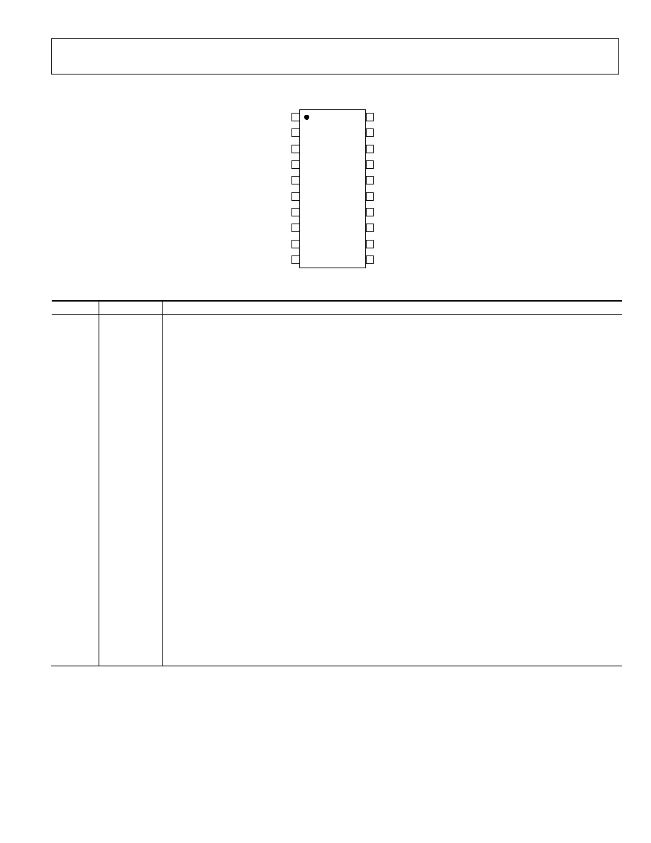
PIN CONFIGURATION AND FUNCTION DESCRIPTION
ADP3182
TOP VIEW
(Not to Scale)
VCC
FBRTN
FB
COMP
PWRGD
EN
DELAY
RT
RAMPADJ
ILIMIT
PWM1
PWM2
PWM3
SW1
SW2
SW3
GND
CSCOMP
CSSUM
CSREF
1
2
3
20
19
18
4
8
10
5
6
7
13
16
15
14
9
11
12
17
04938-003
Figure 3. Pin Configuration
Table 3. Pin Function Descriptions
Pin No.
Mnemonic
Description
1
VCC
Supply Voltage for the Device.
2
FBRTN
Feedback Return. Voltage error amplifier reference for remote sensing of the output voltage.
3
FB
Feedback Input. Error amplifier input for remote sensing of the output voltage. An external resistor divider
between the output and FBRTN connected to this pin sets the output voltage point. This pin is also the reference
point for the power good and crowbar comparators.
4 COMP Error
Amplifier
Output and Compensation Point.
5
PWRGD
Power Good Output. Open-drain output that signals when the output voltage is outside the proper operating
range.
6
EN
Power Supply Enable Input. Pulling this pin to GND disables the PWM outputs and pulls the PWRGD output low.
7
DELAY
Soft Start Delay and Current Limit Latch-Off Delay Setting Input. An external resistor and capacitor connected
between this pin and GND sets the soft start, ramp-up time and the overcurrent latch-off delay time.
8
RT
Frequency Setting Resistor Input. An external resistor connected between this pin and GND sets the oscillator
frequency of the device.
9
RAMPADJ
PWM Ramp Current Input. An external resistor from the converter input voltage to this pin sets the internal
PWM ramp.
10
ILIMIT
Current Limit Setpoint/Enable Output. An external resistor from this pin to GND sets the current limit threshold
of the converter. This pin is actively pulled low when the ADP3182's EN input is low, or when VCC is below its
UVLO threshold, to signal to the driver IC that the driver high-side and low-side outputs should go low.
11
CSREF
Current Sense Reference Voltage Input. The voltage on this pin is used as the reference for the current sense
amplifier. This pin should be connected to the common point of the output inductors.
12
CSSUM
Current Sense Summing Node. External resistors from each switch node to this pin sum the average inductor
currents together to measure the total output current.
13
CSCOMP
Current Sense Compensation Point. A resistor and a capacitor from this pin to CSSUM determines the gain of the
current sense amplifier.
14
GND
Ground. All internal biasing and the logic output signals of the device are referenced to this ground.
15 to 17
SW3 to SW1
Current Balance Inputs. Inputs for measuring the current level in each phase. The SW pins of unused phases
should be left open.
18 to 20
PWM3 to
PMW1
Logic-Level PWM Outputs. Each output is connected to the input of an external MOSFET driver such as the
ADP3418. Connecting the PWM3 output to GND causes that phase to turn off, allowing the ADP3182 to operate
as a 1- or 2-phase controller.
ADP3182
Rev. 0 | Page 8 of 20
TYPICAL PERFORMANCE CHARACTERISTICS
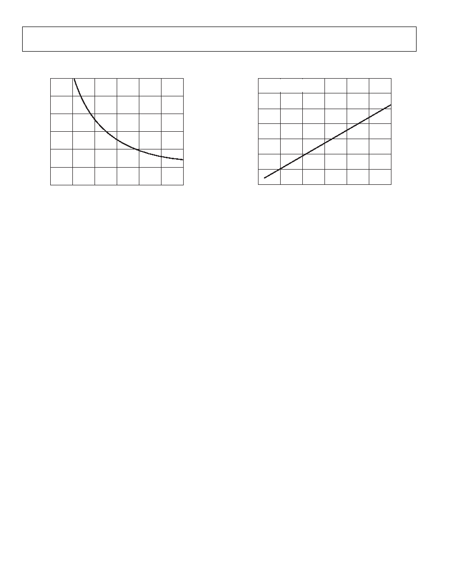
3
2
1
0
MAS
T
E
R
CLOCK FRE
Q
UE
NCY
(MHz)
R
T
VALUE (k
)
0
250
200
150
100
50
300
04938-004
Figure 4. Master Clock Frequency vs. RT
5.4
5.3
5.2
5.1
5.0
4.9
4.8
4.7
S
U
P
P
L
Y
CURRE
NT (mA)
OSCILLATOR FREQUENCY (MHz)
T
A
= 25∫C
3-PHASE OPERATION
0
2.5
2.0
1.5
1.0
0.5
3.0
04938-005
Figure 5. Supply Current vs. Oscillator Frequency

ADP3182
Rev. 0 | Page 9 of 20
THEORY OF OPERATION
The ADP3182 combines a multimode, fixed frequency PWM
control with multiphase logic outputs for use in 1-, 2-, and
3-phase, synchronous, buck, point-of-load supply power
converters. Multiphase operation is important for producing the
high currents and low voltages demanded by auxiliary supplies
in desktop computers, workstations, and servers. Handling the
high currents in a single-phase converter would place high
thermal demands on the components in the system, such as the
inductors and MOSFETs.
The multimode control of the ADP3182 ensures a stable, high
performance topology for
∑
Balancing currents and thermals between phases
∑
High speed response at the lowest possible switching
frequency and output decoupling
∑
Minimizing thermal switching losses due to lower
frequency operation
∑
Tight regulation and accuracy
∑
Reduced output ripple due to multiphase cancellation
∑
PC board layout noise immunity
∑
Ease of use and design due to independent component
selection
∑
Flexibility in operation for tailoring design to low cost or
high performance
START-UP SEQUENCE
During start-up, the number of operational phases and their
phase relationship is determined by the internal circuitry that
monitors the PWM outputs. Normally, the ADP3182 operates
as a 3-phase PWM controller. Grounding the PWM3 pin
programs 1/2-phase operation.
When the ADP3182 is enabled, the controller outputs a voltage
on PWM3 that is approximately 675 mV. An internal comparator
checks the pin's voltage vs. a threshold of 300 mV. If the pin is
grounded, it is below the threshold and the phase is disabled.
The output resistance of the PWM pin is approximately 5 k
during this detection time. Any external pull-down resistance
connected to the PWM pin should be more than 25 k to
ensure proper operation. PWM1 and PWM2 are disabled
during the phase detection interval, which occurs during the
first two clock cycles of the internal oscillator. After this time, if
the PWM output is not grounded, the 5 k resistance is
removed, and the PWM output switches between 0 V and 5 V. If
the PWM output is grounded, it remains off.
The PWM outputs are logic-level devices intended for driving
external gate drivers such as the ADP3418. Because each phase
is monitored independently, operation approaching 100% duty
cycle is possible. Also, more than one output can be on at the
same time for overlapping phases.
MASTER CLOCK FREQUENCY
The clock frequency of the ADP3182 is set with an external
resistor connected from the RT pin to ground. The frequency
follows the graph in Figure 4. To determine the frequency per
phase, the clock is divided by the number of phases in use. If
PWM3 is grounded, then divide the master clock by 2 for the
frequency of the remaining two phases.
It is important to note that if only one phase is used, the clock
will switch as if two phases were operating. This means that the
oscillator frequency must be set at twice the expected value to
program the desired PWM frequency.
OUTPUT VOLTAGE DIFFERENTIAL SENSING
The ADP3182 uses a differential-sensing, low offset voltage error
amplifier. This maintains a worst-case specification of ±2%
differential-sensing error over its full operating output voltage
and temperature range. The output voltage is sensed between
the FB and FBRTN pins. FB should be connected through a
resistor to the regulation point, usually the local bypass
capacitor for the load. FBRTN should be connected directly to
the remote sense ground point. The internal precision reference
is referenced to FBRTN, which has a minimal current of 100 µA
to allow accurate remote sensing. The internal error amplifier
compares the output of the reference to the FB pin to regulate
the output voltage.
OUTPUT CURRENT SENSING
The ADP3182 provides a dedicated current sense amplifier
(CSA) to monitor the total output current for current limit
detection. Sensing the load current at the output gives the total
average current being delivered to the load, which is an
inherently more accurate method than peak current detection
or sampling the current across a sense element such as the low-
side MOSFET. This amplifier can be configured several ways
depending on the objectives of the system:
∑
Output inductor DCR sensing without a thermistor for
lowest cost
∑
Output inductor DCR sensing with a thermistor for
improved accuracy for tracking inductor temperature
∑
Sense resistors for highest accuracy measurements
The positive input of the CSA is connected to the CSREF pin,
which is connected to the output voltage. The inputs to the
amplifier are summed together through resistors from the
sensing element (such as the switch node side of the output
inductors) to the inverting input, CSSUM. The feedback resistor
between CSCOMP and CSSUM sets the gain of the amplifier,
and a filter capacitor is placed in parallel with this resistor. The
ADP3182
Rev. 0 | Page 10 of 20
gain of the amplifier is programmable by adjusting the feedback
resistor. The current information is then given as the difference
of CSREF - CSCOMP. This difference in signal is used as a
differential input for the current limit comparator.
To provide the best accuracy for sensing current, the CSA is
designed to have a low offset input voltage. In addition, the
sensing gain is determined by external resistors so that the gain
can be made extremely accurate.
CURRENT CONTROL MODE AND
THERMAL BALANCE
The ADP3182 has individual inputs for each phase that are used
for monitoring the current in each phase. This information is
combined with an internal ramp to create a current balancing
feedback system, which has been optimized for initial current
balance accuracy and dynamic thermal balancing during
operation. This current balance information is independent of
the average output current information used for the current
limit described previously.
The magnitude of the internal ramp can be set to optimize the
transient response of the system. It also monitors the supply
voltage for feed-forward control to compensate for changes in
the supply voltage. A resistor connected from the power input
voltage to the RAMPADJ pin determines the slope of the
internal PWM ramp. External resistors can be placed in series
with individual phases to create, if desired, an intentional
current imbalance such as when one phase may have better
cooling and can support higher currents. Resistors R
SW1
through
R
SW3
(see the typical application circuit in Figure 9) can be used
for adjusting thermal balance. Add placeholders for these
resistors during the initial layout so that adjustments can be made
after completing thermal characterization of the design.
To increase the current in any given phase, increase R
SW
for that
phase (set R
SW
= 0 for the hottest phase and do not change it
during balancing). Increasing R
SW
to only 500 substantially
increases the phase current. Increase each R
SW
value by small
amounts to achieve balance, starting with the coolest phase.
VOLTAGE CONTROL MODE
A high gain-bandwidth voltage mode error amplifier is used for
the voltage-mode control loop. The control input voltage to the
positive input is derived from the internal 800 mV reference.
The output of the amplifier is the COMP pin, which sets the
termination voltage for the internal PWM ramps.
The negative input (FB) is tied to the center point of a resistor
divider from the output sense location. The main loop
compensation is incorporated into the feedback network
between FB and COMP.
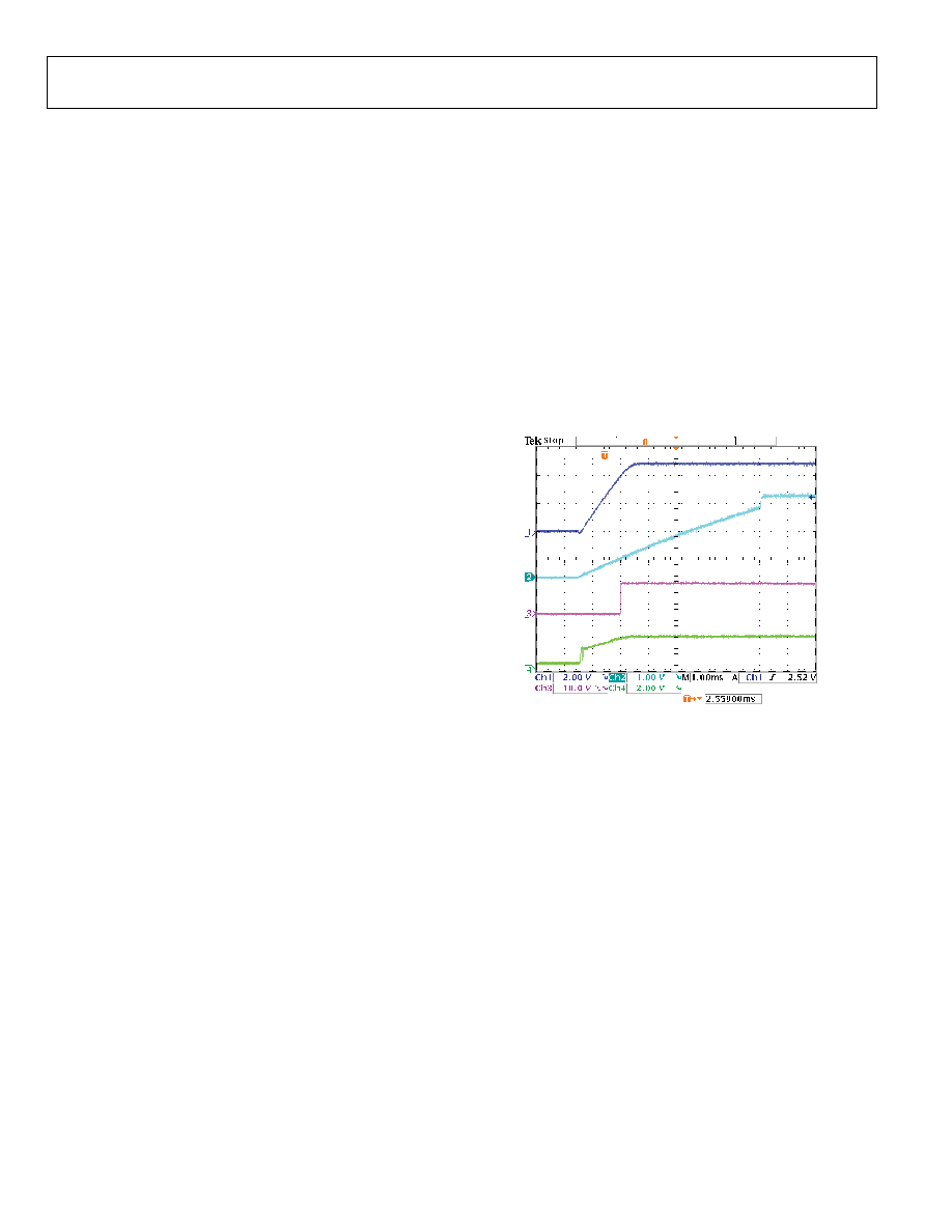
SOFT START
The power-on, ramp-up time of the output voltage is set with a
capacitor and resistor in parallel from the DELAY pin to ground.
The RC time constant also determines the current limit latch-
off time as explained in the following section. In UVLO or
when EN is logic low, the DELAY pin is held at ground. After
the UVLO threshold is reached and EN is logic high, the
DELAY capacitor is charged with an internal 20 µA current
source. The output voltage follows the ramping voltage on the
DELAY pin, limiting the inrush. The soft start time depends on
the value of C
DLY
, with a secondary effect from R
DLY
.
If either EN is taken low or VCC drops below UVLO, the
DELAY capacitor is reset to ground to prepare for another soft
start cycle. Figure 6 shows a typical soft start sequence for the
ADP3182.
04938-006
Figure 6. Typical Start-Up Waveforms
Channel 1: CSREF, Channel 2: DELAY,
Channel 3: PWRGD, Channel 4: COMP
CURRENT LIMIT, SHORT-CIRCUIT, AND
LATCH-OFF PROTECTION
The ADP3182 compares a programmable current limit setpoint
to the voltage from the output of the current sense amplifier.
The level of current limit is set with the resistor from the ILIMIT
pin to ground. During normal operation, the voltage on ILIMIT
is 3 V. The current through the external resistor is internally
scaled to produce a current limit threshold of 10.4 mV/µA. If
the difference in voltage between CSREF and CSCOMP rises
above the current limit threshold, the internal current limit
amplifier controls the internal COMP voltage to maintain the
average output current at the limit.

ADP3182
Rev. 0 | Page 11 of 20
After the limit is reached, the 3 V pull-up on the DELAY pin is
disconnected, and the external delay capacitor is discharged
through the external resistor. A comparator monitors the DELAY
voltage and shuts off the controller when the voltage drops
below 1.8 V. The current limit latch-off delay time is therefore
set by the RC time constant discharging from 3 V to 1.8 V.
Typical overcurrent latch-off waveforms are shown in Figure 7.
Because the controller continues to cycle the phases during the
latch-off delay time, the controller returns to normal operation
if the short is removed before the 1.8 V threshold is reached.
The recovery characteristic depends on the state of PWRGD. If
the output voltage is within the PWRGD window, the controller
resumes normal operation. However, if a short circuit has
caused the output voltage to drop below the PWRGD threshold,
a soft start cycle is initiated.
The latch-off function can be reset by either removing and
reapplying VCC to the ADP3182, or by pulling the EN pin low
for a short time. To disable the short-circuit latch-off function,
the external resistor to ground should be left open, and a high-
value (>1 M) resistor should be connected from DELAY to
VCC. This prevents the DELAY capacitor from discharging, so
the 1.8 V threshold is never reached. The resistor has an impact
on the soft start time because the current through it adds to the
internal 20 µA current source.
During start-up when the output voltage is below 200 mV, a
secondary current limit is active. This is necessary because the
voltage swing of CSCOMP cannot go below ground. This
secondary current limit controls the internal COMP voltage to
the PWM comparators to 2 V. This limits the voltage drop
across the low-side MOSFETs through the current balance
circuitry.
An inherent per phase current limit protects individual phases
if one or more phases stop functioning because of a faulty
component. This limit is based on the maximum normal mode
COMP voltage.
POWER GOOD MONITORING
The power good comparator monitors the output voltage via the
FB pin. The PWRGD pin is an open-drain output whose high
level (when connected to a pull-up resistor) indicates that the
output voltage is within the nominal limits specified in the
electrical table. PWRGD goes low if the output voltage is
outside this specified range or the EN pin is pulled low. Figure 8
shows the PWRGD output response when the input power is
removed from the regulator.
04938-007
Figure 7. Overcurrent Latch-Off Waveforms
Channel 1: CSREF, Channel 2: COMP,
Channel 3: Phase 1 Switch Node, Channel 4: DELAY
04938-008
Figure 8. Shutdown Waveforms
Channel 1: CSREF, Channel 2: DELAY,
Channel 3: PWRGD, Channel 4: COMP
OUTPUT CROWBAR
As part of the protection for the load and output components of
the supply, the PWM outputs are driven low (turning on the
low-side MOSFETs) when the output voltage exceeds the upper
crowbar threshold. This crowbar action stops once the output
voltage falls below the release threshold of approximately 650 mV.
Turning on the low-side MOSFETs pulls down the output as the
reverse current builds up in the inductors. If the output over-
voltage is due to a short in the high-side MOSFET, this action
limits the current of the input supply or blows the fuse to
protect the microprocessor from being destroyed.

ADP3182
Rev. 0 | Page 12 of 20
OUTPUT ENABLE AND UVLO
For the ADP3182 to begin switching, the input supply (VCC) to
the controller must be higher than the UVLO threshold, and
the EN pin must be higher than its logic threshold. If UVLO is
less than the threshold or the EN pin is logic low, the ADP3182 is
disabled. This holds the PWM outputs at ground, shorts the
DELAY capacitor to ground, and holds the ILIMIT pin at ground.
In the application circuit, the ILIMIT pin should be connected
to the OD pins of the ADP3418 drivers. The ILIMIT being
grounded disables the drivers such that both DRVH and DRVL
are grounded. This feature is important in preventing the
discharge of the output capacitors when the controller is shut
off. If the driver outputs were not disabled, a negative voltage
could be generated during output due to the high current
discharge of the output capacitors through the inductors.
ADP3182
Rev. 0 | Page 13 of 20
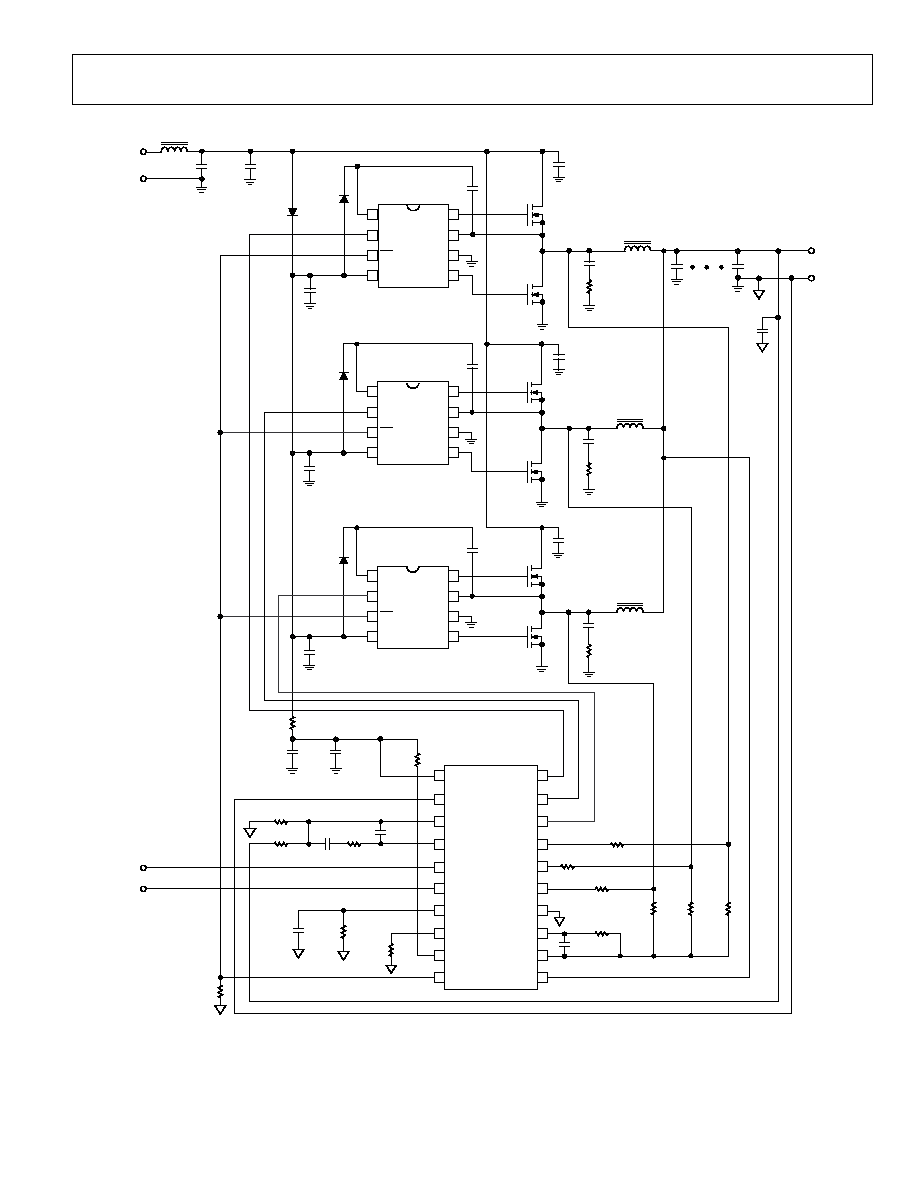
04938-009
1
2
3
4
5
6
7
8
BST
IN
OD
V
CC
DRVH
SW
PGND
DRVL
U2
ADP3418
+
+
D2
1N4148WS
C3
1
µ
F
C2
2700
µ
F
16V
C1
2700
µ
F
16V
L1
1
µ
H
V
IN
12V
V
IN
RTN
C4
100nF
Q1
NTD40N02
C5
4.7
µ
F
Q2
NTD110N02
C6
4.7nF
R1
2.2
1
2
3
4
5
6
7
8
BST
IN
OD
V
CC
DRVH
SW
PGND
DRVL
U3
ADP3418
D3
1N4148WS
C7
1
µ
F
C8
100nF
Q3
NTD40N02
C9
4.7
µ
F
Q4
NTD110N02
C10
4.7nF
R2
2.2
1
2
3
4
5
6
7
8
BST
IN
OD
V
CC
DRVH
SW
PGND
DRVL
U4
ADP3418
D4
1N4148WS
C11
1
µ
F
C12
100nF
Q5
NTD40N02
C13
4.7
µ
F
Q6
NTD110N02
L4
600nH/1.4m
C14
4.7nF
R3
2.2
L3
600nH/1.4m
+
C17
+
C21
V
OUT
1.8V
55A
V
OUT
RTN
4.7
µ
F
◊
10
6.3V
MLCC
L2
600nH/1.4m
1200
µ
F/6.3V
◊
5
15m
ESR (EACH)
R
R
332k
R4
10
C15
1
µ
F
C16
33
µ
F
1
2
4
5
16
17
19
20
V
CC
FBRTN
COMP
PWRGD
PWM1
PWM2
SW1
SW2
U1
ADP3182
10
11
ILIMIT
CSREF
9
12
RAMPADJ
CSSUM
8
13
RT
CSCOMP
7
14
DELAY
GND
6
15
EN
SW3
3
18
FB
PWM3
R
PH3
140k
R
PH1
140k
R
PH2
140k
POWER
GOOD
ENABLE
R
LIM
287k
C
DLY
39nF
R
DLY
470k
R
T
258k
R
B2
1.24k
R
B1
1.00k
C
A
1.2nF
R
A
6.04k
C
FB
100pF
R
CS
100k
C
CS
5.6nF
R
SW3
*
R
SW1
*
R
SW2
*
+
D1
1N4148WS
Figure 9. 1.8 V, 55 A Application Circuit

ADP3182
Rev. 0 | Page 14 of 20
APPLICATIONS
The design parameters for the typical high current point-of-
load dc/dc buck converter shown in Figure 9 are as follows:
∑
Input voltage (V
IN
) = 12 V
∑
VID setting voltage (V
OUT
) = 1.8 V
∑
Duty cycle (D) = 0.15
∑
Output current I
O
= 55 A
∑
Maximum output current (I
LIM
) = 110 A
∑
Number of phases (n) = 3
∑
Switching frequency per phase (f
SW
) = 250 kHz
SETTING THE CLOCK FREQUENCY
The ADP3182 uses a fixed-frequency control architecture. The
frequency is set by an external timing resistor (R
T
). The clock
frequency and the number of phases determine the switching
frequency per phase, which relates directly to switching losses
and the sizes of the inductors and the input and output
capacitors. With n = 3 for three phases, a clock frequency of
750 kHz sets the switching frequency (f
SW
) of each phase to
250 kHz, which represents a practical trade-off between the
switching losses and the sizes of the output filter components.
Equation 1 shows that to achieve a 750 kHz oscillator frequency,
the correct value for R
T
is 256 k. Alternatively, the value for R
T
can be calculated using
k
27
pF
4.7
1
-
◊
◊
=
SW
T
f
n
R
(1)
k
256
k
27
pF
4.7
kHz
250
3
1
=
-
◊
◊
=
T
R
where 4.7 pF and 27 k are internal IC component values. For
good initial accuracy and frequency stability, a 1% resistor is
recommended. The closest standard 1% value for this design is
258 k.
SOFT START AND CURRENT LIMIT LATCH-OFF
DELAY TIME
Because the soft start and current limit latch-off delay functions
share the DELAY pin, these two parameters must be considered
together. The first step is to set C
DLY
for the soft start ramp. This
ramp is generated with a 20 µA internal current source. The
value of R
DLY
has a second-order impact on the soft start time
because it sinks part of the current source to ground. However,
as long as R
DLY
is kept greater than 200 k, this effect is minor.
The value for C
DLY
can be approximated using
OUT
SS
DLY
OUT
DLY
V
t
R
V
C
◊
◊
-
=
2
A
20
(2)
where:
t
SS
is the desired soft start time.
Assuming an R
DLY
of 390 k and a desired soft start time of 3
ms, C
DLY
is 36 nF.
The closest standard value for C
DLY
is 39 nF.
Once C
DLY
is chosen, R
DLY
can be calculated for the current limit
latch-off time using
DLY
DELAY
DLY
C
t
R
◊
=
96
.
1
(3)
If the result for R
DLY
is less than 200 k, a smaller soft start time
should be considered by recalculating the equation for C
DLY
, or a
longer latch-off time should be used. R
DLY
should never be less
than 200 k. In this example, a delay time of 9 ms results in
R
DLY
= 452 k. The closest standard 5% value is 470 k.
INDUCTOR SELECTION
The amount of inductance determines the ripple current in the
inductor. Less inductance leads to more ripple current, which
increases the output ripple voltage and conduction losses in the
MOSFETs, but allows using smaller inductors and, for a
specified peak- peak transient deviation, less total output
capacitance. Conversely, a higher inductance means lower
ripple current and reduced conduction losses, but requires
larger inductors and more output capacitance for the same
peak-peak transient deviation. In any multiphase converter, a
practical value for the peak-peak inductor ripple current is less
than 50% of the maximum dc current in the same inductor.
Equation 4 shows the relationship between the inductance,
oscillator frequency, and peak-peak ripple current in the
inductor.
Equation 5 can be used to determine the minimum inductance
based on a given output ripple voltage.
(
)
L
f
D
V
I
SW
OUT
R
◊
-
◊
=
1
(4)
(
)
(
)
RIPPLE
SW
x
OUT
V
f
D
n
R
V
L
◊
◊
-
◊
◊
1
(5)
where:
R
X
is ESR of output bulk capacitors.

ADP3182
Rev. 0 | Page 15 of 20
Solving Equation 5 for a 20 mV p-p output ripple and an R
X
of
3 m voltage yields
(
)
nH
594
mV
0
2
kHz
0
25
15
0.
3
1
m
3
V
8
1.
=
◊
◊
-
◊
◊
L
If the resulting ripple voltage is too low, the level of inductance
can be decreased until the desired ripple value is met. This
allows optimal transient response and minimum output
decoupling.
The smallest possible inductor should be used to minimize the
number of output capacitors. For this example, choosing a
600 nH inductor is a good starting point that produces a
calculated ripple current of 6.6 A. The inductor should not
saturate at the peak current of 21.6 A and should be able to
handle the sum of the power dissipation caused by the average
current of 18.3 A in the winding and core loss.
Another important factor in the inductor design is the DCR,
which is used for measuring the phase currents. A large DCR
can cause excessive power losses, whereas too small a value can
lead to increased measurement error. For this design, a DCR of
1.4 m was chosen.
Designing an Inductor
Once the inductance and DCR are known, the next step is to
either design an inductor or find a standard inductor that
comes as close as possible to meeting the overall design goals.
The first decision in designing the inductor is to choose the
core material. Several possibilities for providing low core loss at
high frequencies include the powder cores (e.g., Kool-MµÆ from
Magnetics, Inc., or from Micrometals) and the gapped soft
ferrite cores (e.g., 3F3 or 3F4 from Philips). Low frequency
powdered iron cores should be avoided, especially when the
inductor value is relatively low and the ripple current is high, due
to their high core loss.
The best choice for a core geometry is a closed-loop type such
as a potentiometer core, a PQ, U, or E core, or a toroid core. A
good compromise between price and performance is a core with
a toroidal shape.
Many useful references for magnetics design are available for
quickly designing a power inductor, such as
∑
Magnetic Designer Software
Intusoft (www.intusoft.com)
∑
Designing Magnetic Components for High-Frequency DC-
DC Converters, by William T. McLyman, Kg Magnetics,
Inc., ISBN 1883107008
Selecting a Standard Inductor
The following power inductor manufacturers can provide design
consultation and deliver power inductors optimized for high
power applications upon request.
∑
Coilcraft
(847) 639-6400
www.coilcraft.com
∑
Coiltronics
(561) 752-5000
www.coiltronics.com
∑
Sumida Electric Company
(510) 668-0660
www.sumida.com
∑
Vishay Intertechnology
(402) 563-6866
www.vishay.com
OUTPUT CURRENT SENSE
The output current can be measured by summing the voltage
across each inductor and passing the signal through a low-pass
filter. The CS amplifier is configured with resistors R
PH(X)
(for
summing the voltage), and R
CS
and C
CS
(for the low-pass filter).
The output current I
O
is set by the following equations:
L
DRP
CS
x
PH
O
R
V
R
R
I
◊
=
)
(
(6)
CS
L
CS
R
R
L
C
◊
(7)
where:
R
L
is the DCR of the output inductors.
V
DRP
is the voltage drop from CSCOMP to CSREF.
When load current reaches its limit, V
DRP
is at its maximum
(V
DRPMAX
). V
DRPMAX
can be in the range of 100 to 200 mV. In this
example, it is 110 mV.
One has the flexibility of choosing either R
CS
or R
PH(X)
. It is
recommended to select R
CS
equal to 100 k, and then solve for
R
PH(X)
by rearranging Equation 6.
( )
( )
k
140
mV
110
110A
k
100
m
4
.
1
=
◊
◊
=
◊
◊
=
x
PH
DRPMAX
LIM
CS
L
x
PH
R
V
I
R
R
R

ADP3182
Rev. 0 | Page 16 of 20
The closest standard 1% value for R
PH(X)
is 140 k. Next, use
Equation 7 to solve for C
CS
.
nF
29
.
4
k
100
m
4
.
1
nH
600
◊
CS
C
Choose the closest standard value that is greater than the result
given by Equation 7. This example uses a C
CS
value of 5.6 nF.
OUTPUT VOLTAGE
ADP3182 has an internal FBRTN voltage reference V
REF
of
800 mV. The output voltage can be set up using a voltage
divider made up of resistors R
B1
and R
B2
:
REF
B
B
B
OUT
V
R
R
R
V
◊
+
=
1
2
1
(8)
Rearranging Equation 8 to solve for R
B2
using the ADP3182
with an internal FB voltage of 800 mV and assuming a 1%, 1 k
resistor for R
B1
yields
=
◊
-
=
◊
-
=
k
25
.
1
k
1
1
V
8
.
0
V
8
.
1
1
1
2
B
REF
OUT
B
R
V
V
R
The closest standard 1% resistor value for R
B2
is 1.24 k.
POWER MOSFETS
For this example, one high-side, N-channel power MOSFET
and two low-side, N-channel power MOSFETs per phase have
been selected. The main selection parameters for the power
MOSFETs are V
GS(TH)
, Q
G
, C
ISS
, C
RSS
, and R
DS(ON)
. The minimum
gate drive voltage (the supply voltage to the ADP3418) dictates
whether standard threshold or logic-level threshold MOSFETs
must be used. With V
GATE
~10 V, logic-level threshold MOSFETs
(V
GS(TH)
< 2.5 V) are recommended.
The maximum output current (I
O
) determines the R
DS(ON)
requirement for the low-side (synchronous) MOSFETs. With
the ADP3182, currents are balanced between phases, thus the
current in each low-side MOSFET is the output current divided
by the total number of MOSFETs (n
SF
). With conduction losses
being dominant, the following expression shows the total power
being dissipated in each synchronous MOSFET in terms of the
ripple current per phase (I
R
) and the average total output current
(I
O
):
(
)
( )
SF
DS
SF
R
SF
O
SF
R
n
I
n
n
I
D
P
◊
◊
+
◊
-
=
2
2
12
1
1
(9)
Knowing the maximum output current and the maximum
allowed power dissipation, one can determine the required
R
DS(ON)
for the MOSFET. For D-PAK MOSFETs up to an
ambient temperature of 50∞C, a safe limit for P
SF
is 1 W to 1.5 W
at 120∞C junction temperature. Therefore, for this example,
R
DS(SF)
(per MOSFET) < 7.5 m. This R
DS(SF)
is also at a junction
temperature of about 120∞C, so one must account for this when
making this selection. This example uses a lower-side MOSFET
with 4.8 m at 120∞C.
Another important factor for the synchronous MOSFET is the
input capacitance and feedback capacitance. The ratio of
feedback to input must be small (less than 10% is recom-
mended) to prevent accidentally turning on the synchronous
MOSFETs when the switch node goes high.
Also, the time to switch the synchronous MOSFETs off should
not exceed the nonoverlap dead time of the MOSFET driver
(40 ns typical for the ADP3418). The output impedance of the
driver is approximately 2 , and the typical MOSFET input gate
resistances are about 1 to 2 ; therefore, one should adhere to
a total gate capacitance of less than 6000 pF. Because there are
two MOSFETs in parallel, the input capacitance for each
synchronous MOSFET should be limited to 3000 pF.
The high-side (main) MOSFET must handle two main power
dissipation components: conduction and switching losses. The
switching loss is related to the amount of time for the main
MOSFET to turn on and off, and to the current and voltage that
are being switched. Basing the switching speed on the rise and
fall time of the gate driver impedance and MOSFET input
capacitance, the following expression provides an approximate
value for the switching loss per main MOSFET:
(
)
ISS
MF
G
MF
O
CC
SW
MF
S
C
n
n
R
n
I
V
f
P
◊
◊
◊
◊
◊
◊
= 2
(10)
where:
n
MF
is the total number of main MOSFETs.
R
G
is the total gate resistance (2 for the ADP3418 and about
1 for typical high speed switching MOSFETs, making R
G
= 3 ).
C
ISS
is the input capacitance of the main MOSFET.
Note that adding more main MOSFETs (n
MF
) does not help the
switching loss per MOSFET because the additional gate
capacitance slows switching. The most efficient way to reduce
switching loss is to use lower gate capacitance devices.
The conduction loss of the main MOSFET is given by the
following equation:
(
)
(
)
MF
DS
MF
R
MF
MF
C
R
n
I
n
n
D
P
◊
◊
◊
+
◊
=
2
2
O
12
1
I
(11)
where:
R
DS(MF)
is the on resistance of the MOSFET.
Typically, for main MOSFETs, the highest speed (low C
ISS
)
device is preferred, but faster devices usually have higher on
resistance. Select a device that meets the total power dissipation

ADP3182
Rev. 0 | Page 17 of 20
(about 1.5 W for a single D-PAK) when combining the
switching and conduction losses.
For this example, an NTD40N03L was selected as the main
MOSFET (three total; n
MF
= 3), with a C
ISS
= 584 pF (max) and
R
DS(MF)
= 19 m (max at T
J
= 120∞C), and an NTD110N02L was
selected as the synchronous MOSFET (three total; n
SF
= 3), with
C
ISS
= 2710 pF (max) and R
DS(SF)
= 4.8 m (max at T
J
= 120∞C).
The synchronous MOSFET C
ISS
is less than 3000 pF, satisfying
that requirement. Solving for the power dissipation per MOSFET
at I
O
= 55 A and I
R
= 6.6 A yields 894 mW for each synchronous
MOSFET and 1.16 W for each main MOSFET. These numbers
comply with the guideline to limit the power dissipation to
around 1 W per MOSFET.
One last thing to consider is the power dissipation in the driver
for each phase. This is best described in terms of the Q
G
for the
MOSFETs and is given by the following equation:
(
)
CC
CC
GSF
SF
GMF
MF
SW
DRV
V
I
Q
n
Q
n
n
f
P
◊
+
◊
+
◊
◊
◊
=
2
(12)
where:
Q
GMF
is the total gate charge for each main MOSFET.
Q
GSF
is the total gate charge for each synchronous MOSFET.
Also shown is the standby dissipation factor (I
CC
◊ V
CC
) for the
driver. For the ADP3418, the maximum dissipation should be
less than 400 mW. In this example, with I
CC
= 7 mA, Q
GMF
=
9 nC, and Q
GSF
= 46 nC, there is 165 mW in each driver, which
is below the 400 mW dissipation limit. See the ADP3418 data
sheet for more details.
RAMP RESISTOR SELECTION
The ramp resistor (R
R
) is used for setting the size of the internal
PWM ramp. The value of this resistor is chosen to provide the
best combination of thermal balance, stability, and transient
response. The following expression is used to determine the
optimum value:
k
333
pF
5
m
8
.
4
5
3
nH
0
60
0.2
3
)
)(
(
=
◊
◊
◊
◊
=
◊
◊
◊
◊
=
R
R
SF
ON
DS
D
R
R
R
C
R
A
L
A
R
(13)
where:
A
R
is the internal ramp amplifier gain.
A
D
is the current balancing amplifier gain.
R
DS(ON)(SF)
is the total low-side MOSFET on resistance.
C
R
is the internal ramp capacitor value.
The closest standard 1% resistor value is 332 k.
The internal ramp voltage magnitude can be calculated by using
(
)
(
)
V
m
737
kHz
0
25
pF
5
k
332
V
8
1.
5
0.1
1
0.2
1
=
◊
◊
◊
-
◊
=
◊
◊
◊
-
◊
=
R
SW
R
R
OUT
R
R
V
f
C
R
V
D
A
V
(14)
The size of the internal ramp can be made larger or smaller. If it
is made larger, stability and transient response improve, but
thermal balance degrades. Likewise, if the ramp is made
smaller, thermal balance improves but transient response and
stability degrade. The factor of three in the denominator of
Equation 13 sets a ramp size with optimal balance for good
stability, transient response, and thermal balance.
CURRENT LIMIT SETPOINT
To select the current limit setpoint, first find the resistor value
for R
LIM
. The current limit threshold for the ADP3182 is set
with a 3 V source (V
LIM
) across R
LIM
with a gain of 10.4 mV/µA
(A
LIM
). R
LIM
can be found using
DRPMAX
LIM
LIM
LIM
V
V
A
R
◊
=
(15)
For values of R
LIM
greater than 500 k, the current limit may be
lower than expected and therefore necessitate some adjustment of
R
LIM
. Here, I
LIM
is the average current limit for the output of the
supply. In this example, using the V
DRPMAX
value of 110 mV from
Equations 6 and 7 and choosing a peak current limit of 110 A
for I
LIM
results in R
LIM
= 284 k, for which 287 k is chosen as
the nearest 1% value.
The limit of the per phase current limit described earlier is
determined by
(
)
(
)
2
R
MAX
DS
D
BIAS
R
MAX
COMP
PHLIM
I
R
A
V
V
V
I
+
◊
-
-
(16)
FEEDBACK LOOP COMPENSATION DESIGN
Optimized compensation of the ADP3182 allows the best
possible response of the regulator's output to a load change. The
basis for determining the optimum compensation is to make
the regulator and output decoupling appear as an output
impedance that is entirely resistive over the widest possible
frequency range, including dc.
With the multimode feedback structure of the ADP3182, the
feedback compensation must be set so that the converter's
output impedance, working in parallel with the output
decoupling, will meet this goal. One will need to compensate for
the several poles and zeros created by the output inductor and
decoupling capacitors (output filter).
ADP3182
Rev. 0 | Page 18 of 20
A type three compensator on the voltage feedback is adequate
for proper compensation of the output filter. Equations 20 to 22
are intended to yield an optimal starting point for the design;
some adjustments may be necessary to account for PCB and
component parasitic effects.
DS
D
L
OUT
R
X
B
X
X
A
R
A
R
V
V
R
n
R
R
C
C
◊
+
◊
◊
◊
◊
◊
=
2
4
(17)
◊
◊
◊
-
◊
◊
◊
◊
◊
◊
=
X
SW
DS
D
OUT
X
R
X
X
B
A
R
f
R
A
V
R
V
L
R
C
n
R
R
2
4
2
(18)
A
SW
FB
R
f
n
C
◊
◊
◊
=
2
1
(19)
If C
X
is 6000 µF (five 1200 µF capacitors in parallel) with an
equivalent ESR of 3 m, the equations above give the following
compensation values:
C
A
= 1.33 nF
R
A
= 6.05 k
C
FB
= 110 pF
Using the nearest standard value for each of these components
yields C
A
= 1.2 nF, R
A
= 6.04 k, and C
FB
= 100 pF.
INPUT CAPACITOR SELECTION AND
INPUT CURRENT di/dt
In continuous inductor current mode, the source current of the
high-side MOSFET is approximately a square wave with a duty
ratio equal to n ◊ V
OUT
/V
IN
and an amplitude of one-nth the
maximum output current. To prevent large voltage transients, a
low ESR input capacitor, sized for the maximum rms current,
must be used. The maximum rms capacitor current is given by
A
1
.
9
1
5
0.1
3
1
A
55
15
.
0
1
1
=
-
◊
◊
◊
=
-
◊
◊
◊
=
CRMS
O
CRMS
I
D
N
I
D
I
(20)
Note that manufacturers often base capacitor ripple current
rating on only 2,000 hours of life. Therefore, it advisable to
further derate the capacitor or to choose a capacitor rated at a
higher temperature than required. Several capacitors may be
placed in parallel to meet size or height requirements in the
design. In this example, the input capacitor bank is formed by
two 2,700 µF, 16 V aluminum electrolytic capacitors and three
4.7 µF ceramic capacitors.
To reduce the input current di/dt to a level below the recom-
mended maximum of 0.1 A/µs, an additional small inductor
(L > 370 nH @ 10 A) can be inserted between the converter and
the supply bus. That inductor also acts as a filter between the
converter and the primary power source.
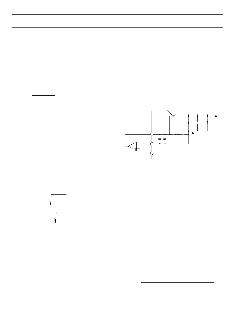
INDUCTOR DCR TEMPERATURE CORRECTION
With the inductor's DCR being used as the sense element and
copper wire being the source of the DCR, one needs to
compensate for temperature changes in the inductor's winding
if a highly accurate safety current limit setpoint is desired.
Fortunately, copper has a well-known temperature coefficient
(TC) of 0.39%/∞C.
If R
CS
is designed to have an opposite and equal percentage of
change in resistance to that of the wire, it cancels the tempera-
ture variation of the inductor's DCR. Due to the nonlinear
nature of NTC thermistors, resistors R
CS1
and R
CS2
are needed.
See Figure 10 for instructions on how to linearize the NTC and
produce the desired temperature tracking.
17
ADP3182
CSCOMP
CSSUM
CSREF
R
TH
R
CS1
R
CS2
C
CS1
C
CS2
R
PH1
R
PH2
R
PH3
TO
SWITCH
NODES
TO
V
OUT
SENSE
PLACE AS CLOSE AS POSSIBLE
TO NEAREST INDUCTOR
OR LOW-SIDE MOSFET
KEEP THIS PATH
AS SHORT AS POSSIBLE
AND WELL AWAY FROM
SWITCH NODE LINES
18
16
04938-010
Figure 10. Temperature Compensation Circuit Values
The following procedures and expressions yield values to use
for R
CS1
, R
CS2
, and R
TH
(the thermistor value at 25∞C) for a given
R
CS
value.
1.
Select an NTC based on type and value. Because we do not
have a value yet, start with a thermistor with a value close
to R
CS
. The NTC should also have an initial tolerance of
better than 5%.
2.
Based on the type of NTC, find its relative resistance value
at two temperatures. The temperatures that work well are
50∞C and 90∞C. These resistance values are called A
(R
TH(50∞C
)/R
TH(25∞C)
) and B (R
TH(90∞C
)/R
TH(25∞C)
). Note that the
NTC's relative value is always 1 at 25∞C.
3.
Find the relative value of R
CS
required for each of these
temperatures. This is based on the percentage of change
needed, which in this example is initially 0.39%/∞C. These
are called r
1
(1/(1 + TC ◊ (T
1
- 25))) and r
2
(1/(1 + TC ◊
(T
2
- 25))), where TC = 0.0039 for copper. T
1
= 50∞C and
T
2
= 90∞C are chosen. From this, one can calculate that r
1
=
0.9112 and r
2
= 0.7978.
4.
Compute the relative values for R
CS1
, R
CS2
, and R
TH
using
(
)
(
)
(
)
(
)
(
)
(
)
B
A
r
A
B
r
B
A
r
A
B
r
B
A
r
r
B
A
r
2
1
1
2
2
1
CS2
-
-
◊
-
◊
-
◊
-
◊
◊
-
◊
+
◊
-
◊
-
◊
◊
-
=
1
1
1
1
(21)

ADP3182
Rev. 0 | Page 19 of 20
(
)
CS2
1
CS2
CS1
r
r
A
r
A
r
-
-
-
-
=
1
1
1
(22)
CS1
CS2
TH
r
r
r
1
1
1
1
-
-
=
(23)
5.
Calculate R
TH
= r
TH
◊ R
CS
, then select the closest value of
thermistor available. Also, compute a scaling factor k based
on the ratio of the actual thermistor value used relative to
the computed one:
(
)
(
)
CALCULATED
TH
ACTUAL
TH
R
R
k =
(24)
6.
Calculate values for R
CS1
and R
CS2
using
CS1
CS
CS1
r
k
R
R
◊
◊
=
(25)
(
)
(
)
(
)
CS2
CS
CS2
r
k
k
R
R
◊
+
-
◊
=
1
(26)
LAYOUT AND COMPONENT PLACEMENT
The following guidelines are recommended for optimal
performance of a switching regulator in a PC system.
General Recommendations
For good results, a PCB with at least four layers is recommended.
This should allow the needed versatility for control circuitry
interconnections with optimal placement, power planes for
ground, input and output power, and wide interconnection
traces in the remainder of the power delivery current paths.
Keep in mind that each square unit of 1 ounce copper trace
has a resistance of ~0.53 m at room temperature.
When high currents must be routed between PCB layers, vias
should be used liberally to create several parallel current paths
so that the resistance and inductance introduced by these current
paths is minimized and the via current rating is not exceeded.
If critical signal lines (including the output voltage sense lines of
the ADP3182) must cross through power circuitry, a signal
ground plane should be interposed between those signal lines
and the traces of the power circuitry. This serves as a shield to
minimize noise injection into the signals at the expense of
making the signal ground a bit noisier.
An analog ground plane should be used around and under the
ADP3182 as a reference for the components associated with the
controller. This plane should be tied to the nearest output de-
coupling capacitor ground, but it should not be tied to any other
power circuitry to prevent power currents from flowing in it.
The components around the ADP3182 should be located close
to the controller with short traces. The most important traces to
keep short and away from other traces are the FB and CSSUM
pins. The output capacitors should be connected as close as
possible to the load or connector. If the load is distributed, the
capacitors should also be distributed and generally be in pro-
portion to where the load tends to be more dynamic. Avoid
crossing any signal lines over the switching power path loop,
described in the following section.
Power Circuitry Recommendations
To minimize radiated switching noise energy (i.e., EMI) and
conduction losses in the board, the switching power path should
be routed on the PCB to encompass the shortest possible length.
Failure to take proper precautions often results in EMI problems
for the entire PC system as well as noise-related operational
problems in the power-converter control circuitry. The switching
power path is the loop formed by the current path through the
input capacitors and the power MOSFETs, including all inter-
connecting PCB traces and planes. Using short and wide
interconnection traces is especially critical in this path for two
reasons: it minimizes the inductance in the switching loop,
which can cause high energy ringing, and it accommodates the
high current demand with minimal voltage loss.
When a power-dissipating component, for example, a power
MOSFET, is soldered to a PCB, the liberal use of vias, both
directly on the mounting pad and immediately surrounding it,
is recommended. Two important reasons for this are improved
current rating through the vias and improved thermal
performance from vias that extend to the opposite side of the
PCB, where a plane can more readily transfer the heat to the air.
To optimize thermal dissipation, make a mirror image of the
pads in use to heat sink the MOSFETs on the opposite side of
the PCB. To further improve thermal performance, use the
largest possible pad area.
The output power path should also be routed to encompass a
short distance. The output power path is formed by the current
path through the inductor, the output capacitors, and the load.
For best EMI containment, a solid power ground plane should
be used as one of the inner layers, extending fully under all the
power components.
Signal Circuitry Recommendations
The output voltage is sensed and regulated between the FB pin
and the FBRTN pin, which connect to the signal ground at the
load. To avoid differential mode noise pickup in the sensed signal,
the loop area should be small. Therefore, the FB and FBRTN
traces should be routed adjacent to each other on top of the
power ground plane back to the controller. The feedback traces
from the switch nodes should be connected as close as possible
to the inductor. The CSREF signal should be connected to the
output voltage at the nearest inductor to the controller.
ADP3182
Rev. 0 | Page 20 of 20
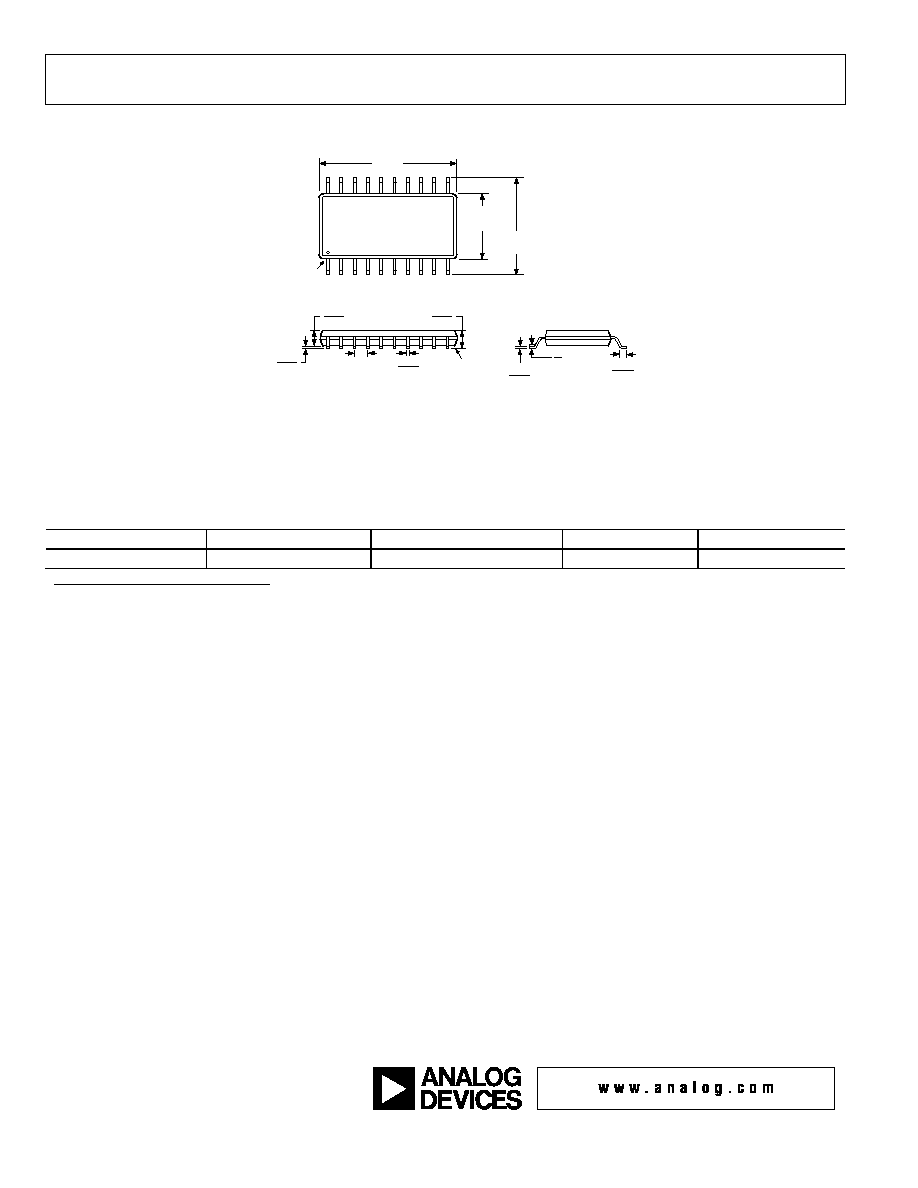
OUTLINE DIMENSIONS
20
11
10
1
PIN 1
8∞
0∞
0.236
BSC
0.154
BSC
0.010
0.004
0.012
0.008
0.025
BSC
COPLANARITY
0.004
0.065
0.049
0.069
0.053
SEATING
PLANE
0.010
0.006
0.050
0.016
0.341
BSC
COMPLIANT TO JEDEC STANDARDS MO-137AD
Figure 11. 20-Lead Shrink Small Outline Package [QSOP]
(RQ-20)
Dimensions shown in inches
ORDERING GUIDE
Model
Temperature Range
Package Description
Package Option
Quantity per Reel
ADP3182JRQZ-RL
1
0∞C to 85∞C
Shrink SOIC 13" Reel
RQ-20
2500
1
Z = Pb-free part.
© 2004 Analog Devices, Inc. All rights reserved. Trademarks and
registered trademarks are the property of their respective owners.
D04938≠0≠10/04(0)