 | –≠–ª–µ–∫—Ç—Ä–æ–Ω–Ω—ã–π –∫–æ–º–ø–æ–Ω–µ–Ω—Ç: ADT7301 | –°–∫–∞—á–∞—Ç—å:  PDF PDF  ZIP ZIP |

13-Bit, ±0.5∞C Accurate, MicroPower Digital
Temperature Sensor in 6-Lead SOT-23
Preliminary Technical Data
ADT7301
Rev. PrJ
Information furnished by Analog Devices is believed to be accurate and reliable.
However, no responsibility is assumed by Analog Devices for its use, nor for any
infringements of patents or other rights of third parties that may result from its use.
Specifications subject to change without notice. No license is granted by implication
or otherwise under any patent or patent rights of Analog Devices. Trademarks and
registered trademarks are the property of their respective owners.
One Technology Way, P.O. Box 9106, Norwood, MA 02062-9106, U.S.A.
Tel: 781.329.4700
www.analog.com
Fax: 781.326.8703
© 2004 Analog Devices, Inc. All rights reserved.
FEATURES
13-bit temperature-to-digital converter
-40∞C to +150∞C operating temperature range
±0.5∞C typical accuracy
0.03125∞C temperature resolution
Shutdown current of 1 µA
Power dissipation of 0.631 mW at V
DD
= 3.3 V
SPI- and DSP-compatible serial interface
Shutdown mode
Space-saving SOT-23 and MSOP packages
APPLICATIONS
Medical equipment
Automotive:
Environmental
controls
Oil
temperature
Hydraulic
systems
Cell phones
Hard disk drives
Personal computers
Electronic test equipment
Office equipment
Domestic appliances
Process control
FUNCTIONAL BLOCK DIAGRAM
SERIAL
BUS
INTERFACE
02884-
0-
001
ADT7301
V
DD
SCLK
DIN
DOUT
GND
13-BIT
ANALOG/DIGITAL
CONVERTER
TEMPERATURE
VALUE
REGISTER
BAND GAP
TEMPERATURE
SENSOR
CS
Figure 1. Functional Block Diagram
GENERAL DESCRIPTION
The ADT7301 is a complete temperature monitoring system
available in SOT-23 and MSOP packages. It contains a band gap
temperature sensor and a 13-bit ADC to monitor and digitize
the temperature reading to a resolution of 0.03125∞C.
The ADT7301 has a flexible serial interface that allows easy
interfacing to most microcontrollers. The interface is compat-
ible with SPIÆ, QSPITM, and MICROWIRETM protocols as well as
DSPs. The part features a standby mode that is controlled via
the serial interface. The ADT7301's wide supply voltage range,
low supply current, and SPI compatible interface make it ideal
for a variety of applications, including personal computers,
office equipment, automotive, and domestic appliances. The
ADT7301 is rated for operation over the -40∞C to +150∞C
temperature range. It is not recommended to operate the device
at temperatures above +125∞C for greater than a total of 5%
(5,000 hours) of the lifetime of the device. Any exposure
beyond this limit will affect device reliability.
PRODUCT HIGHLIGHTS
1.
The ADT7301 has an on-chip temperature sensor that
allows an accurate measurement of the ambient tempera-
ture. The measurable temperature range is -40∞C to
+150∞C.
2.
Supply voltage of 2.7 V to 5.5 V.
3.
Space-saving 6-lead SOT-23 and 8-lead MSOP packages.
4.
Temperature accuracy of ±0.5∞C.
5.
13-bit temperature reading to 0.03125∞C resolution.
6.
The ADT7301 features a shutdown mode that reduces the
power consumption to 4.88 µW with V
DD
= 3.3 V @ 1 SPS.

Preliminary Technical Data
TABLE OF CONTENTS
Specifications..................................................................................... 3
Timing Characteristics................................................................. 4
Absolute Maximum Ratings............................................................ 5
ESD Caution.................................................................................. 5
Pin Configurations and Function Descriptions............................ 6
Typical Performance Characteristics.............................................. 7
Circuit Information .......................................................................... 8
Converter Details.......................................................................... 8
Temperature Value Register ........................................................ 8
Serial Interface .............................................................................. 9
Microprocessor Interfacing....................................................... 10
Mounting The ADT7302........................................................... 12
Supply Decoupling ..................................................................... 12
Outline Dimensions ....................................................................... 13
Ordering Guide............................................................................... 14
REVISION HISTORY
Revision PrE: Preliminary Version
ADT7301
Rev. PrJ | Page 2 of 14

Preliminary Technical Data
ADT7301
SPECIFICATIONS
T
A
= T
MIN
to T
MAX
, V
DD
= 2.7 V to 5.5 V, unless otherwise noted. All specifications apply for ≠40∞C to +150∞C, unless otherwise stated
Table 1. A Grade Specifications
Parameter
Min
Typ
Max Unit Test
Conditions/Comments
TEMPERATURE SENSOR AND ADC
V
DD
= +3.3 V (±10%) and 5 V (±10%)
Accuracy
TBD
±1
∞C
T
A
= 0∞C to 70∞C.
TBD
±2
∞C
T
A
= -20∞C to +85∞C.
TBD
±3
∞C
T
A
= -40∞C to +125∞C.
TBD
±4
1
∞C T
A
= -40∞C to +150∞C.
Temperature Resolution
0.03125
∞C
Auto Conversion Update Rate, t
R
1
sec
Temperature measurement every 1 second
Temperature Conversion Time
2
ms
Thermal Time Constant
2
2
sec
SUPPLIES
Supply Voltage
2.7
5.5
V
For Specified Performance
Supply
Current
Normal Mode
1.6
2.2
mA
V
DD
= 3.3 V. Powered up and converting
190
300
µA
V
DD
= 3.3 V. Powered up and not converting
1.6
2.2
mA
V
DD
= 5 V. Powered up and converting
280
400
µA
V
DD
= 5 V. Powered up and not converting
Shutdown Mode
0.2
1
µA
V
DD
= 3.3 V.
0.2
1
µA
V
DD
= 5 V.
Power
Dissipation
Normal Mode (Average)
631
µW
V
DD
= 3.3 V. Auto conversion update, t
R
.
1.41
mW
V
DD
= +5 V. Auto conversion update, t
R
.
Shutdown Mode (Average)
3
1 sps
4.88
µW
V
DD
= 3.3 V
7.4
µW
V
DD
= 5 V
10 sps
42.9
µW
V
DD
= 3.3 V
65
µW
V
DD
= 5 V
100 sps
423
µW
V
DD
= 3.3 V
641
µW
V
DD
= 5 V
DIGITAL INPUT
4
Input High Voltage, V
IH
2.5
V
Input Low Voltage, V
IL
0.8
V
Input Current, I
IN
±1
µA
V
IN
= 0 V to V
DD
Input Capacitance, C
IN
10
pF
All digital inputs
DIGITAL OUTPUT
5
Output High Voltage, V
OH
V
DD
- 0.3 V
I
SOURCE
= I
SINK
= 200 µA
Output Low Voltage, V
OL
0.4
V
I
OL
= 200 µA
Output Capacitance, C
OUT
50
pF
1
It is not recommended to operate the device at temperatures above +125∞C for greater than a total of 5% (5,000 hours) of the lifetime of the device. Any exposure
beyond this limit will affect device reliability.
2
Thermal Time Constant is the time it takes for a starting temperature difference to change to 36.8% of it's starting value. For example if the ADT7301 experienced a
thermal shock from 0∞C to 100∞C, it would take typically 2 secs for the ADT7301 to reach 63.2∞C.
3
The ADT7301 is taken out of shutdown mode and a temperature conversion is immediately performed after this write operation. Once the temperature conversion is
complete the ADT7301 is put back into shutdown mode.
4
Guaranteed by design and characterization, not production tested.
5
Guaranteed by design and characterization, not production tested.
Specifications subject to change without notice
Rev. PrJ | Page 3 of 14
ADT7301
Preliminary Technical Data
Rev. PrJ | Page 4 of 14
TIMING CHARACTERISTICS
Guaranteed by design and characterization, not production tested. All input signals are specified with tr = tf = 5 ns (10% to 90% of V
DD
)
and timed from a voltage level of 1.6 V.
T
A
= T
MIN
to T
MAX
, V
DD
= 2.7 V to 5.5 V, unless otherwise noted.
Table 2.
Parameter
1
Limit Unit
Comments
t
1
5
ns
min
CS to SCLK Setup Time
t
2
25
ns min
SCLK High Pulse Width
t
3
25
ns min
SCLK Low Pulse Width
t
4
2
35
ns max
Data Access Time after SCLK Falling Edge
t
5
20
ns min
Data Setup Time prior to SCLK Rising Edge
t
6
5
ns min
Data Hold Time after SCLK Rising Edge
t
7
5
ns
min
CS to SCLK Hold Time
t
8
2
40
ns
max
CS to DOUT High Impedance
1
See Figure 13. for SPI Timing diagram.
2
Measured with the load circuit of Figure 2
1.6V
200
µ
A
200
µ
A
I
OH
I
OL
02884-
0-
002
TO
OUTPUT
PIN
C
L
50pF
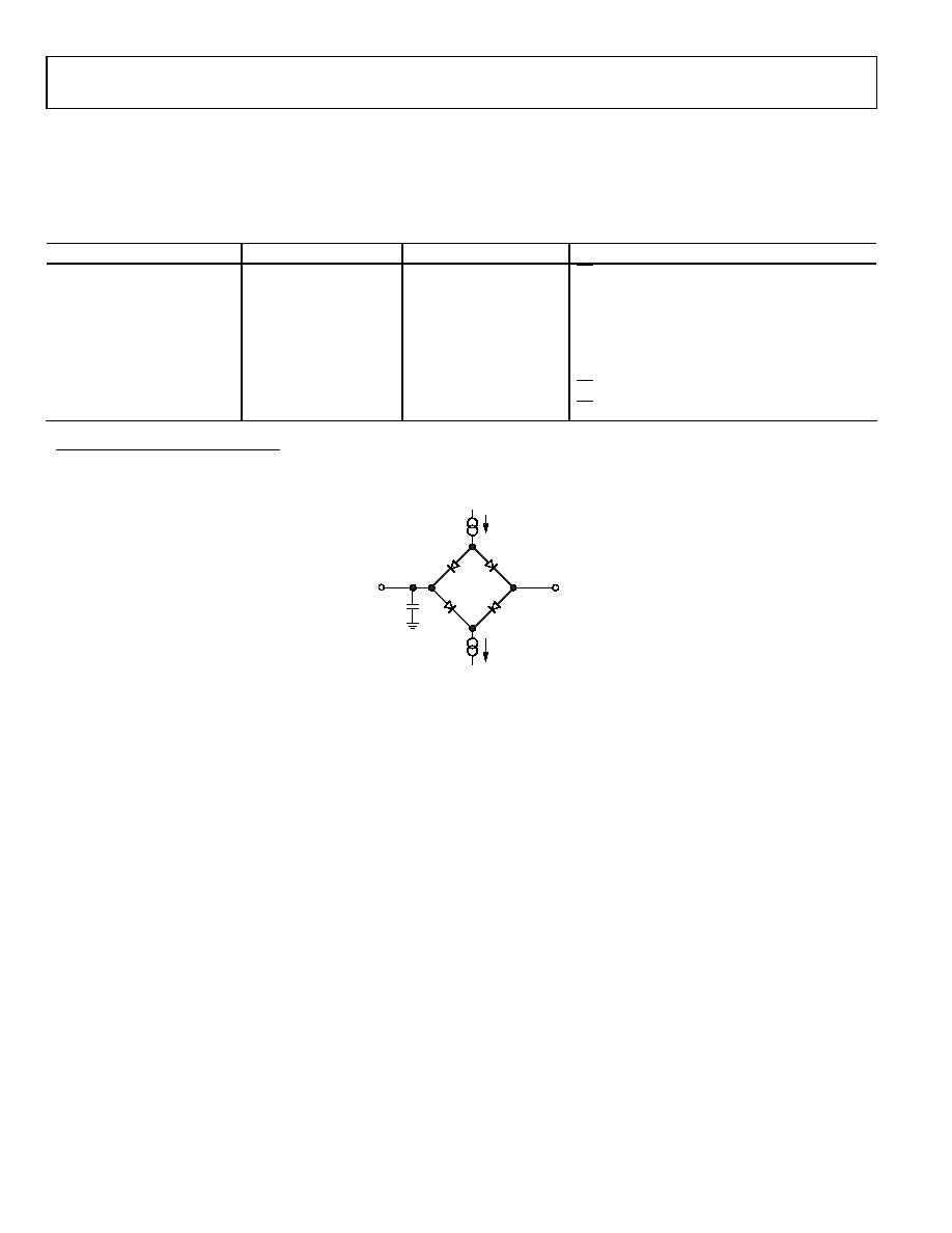
Figure 2. Load Circuit for Data Access Time and Bus Relinquish Time
Preliminary Technical Data
ADT7301
Rev. PrJ | Page 5 of 14
ABSOLUTE MAXIMUM RATINGS
Table 3. ADT7301 Stress Ratings
Parameter Rating
V
DD
to GND
-0.3 V to +7 V
Digital Input Voltage to GND
-0.3 V to V
DD
+ 0.3 V
Digital Output Voltage to GND
-0.3 V to V
DD
+ 0.3 V
Operating Temperature Range
1
-40∞C
to
+150∞C
Storage Temperature Range
-65∞C to +150∞C
Junction Temperature
+150∞C
6-Lead SOT-23 (RJ-6)
Power Dissipation
2
W
MAX
= (T
JMAX
- T
A
3
)/
JA
Thermal Impedance
JA
, Junction-to-Ambient (still air)
190.4∞C/W
8-Lead MSOP (RM-8)
Power Dissipation
2
W
MAX
= (T
JMAX
- T
A
3)
/
JA
Thermal Impedance
4
JA
, Junction-to-Ambient (still air)
205.9∞C/W
JC
, Junction-to-Case
43.74∞C/W
IR Reflow Soldering
Peak Temperature
+220∞C (-0/+5∞C)
Time at Peak Temperature
10 s to 20 s
Ramp-up Rate
2∞C/s to 3∞C/s
Ramp-down Rate
-6∞C/sec
1
It is not recommended to operate the ADT7301 at temperatures above 125∞C
for greater than a total of 5% of the lifetime of the device. Any exposure
beyond this limit will affect device reliability.
2
Values relate to package being used on a standard 2-layer PCB. Reference
Figure 3 for a plot of maximum power dissipation versus ambient
temperature (T
A
).
3
T
A
= ambient temperature
4
Junction-to-case resistance is applicable to components featuring a
preferential flow direction, e.g., components mounted on a heat sink.
Junction-to-ambient resistance is more useful for air-cooled, PCB mounted
components.
Stresses above those listed under Absolute Maximum Ratings
may cause permanent damage to the device. This is a stress
rating only; functional operation of the device at these or any
other conditions above those indicated in the operational
section of this specification is not implied. Exposure to absolute
maximum rating conditions for extended periods may affect
device reliability
0
0.2
0.6
0.4
0.8
1.0
1.2
M
A
XI
M
U
M
PO
WER
D
I
SSI
PA
T
I
O
N
(
W
)
150
140
130
120
110
100
90
80
70
60
50
40
30
20
10
0
≠10
≠20
≠30
≠40
TEMPERATURE (∞C)
02884-
0-
003
SOT-23
MSOP
Figure 3. Plot of Maximum Power Dissipation vs. Temperature
ESD CAUTION
ESD (electrostatic discharge) sensitive device. Electrostatic charges as high as 4000 V readily accumulate on the
human body and test equipment and can discharge without detection. Although this product features
proprietary ESD protection circuitry, permanent damage may occur on devices subjected to high energy
electrostatic discharges. Therefore, proper ESD precautions are recommended to avoid performance
degradation or loss of functionality.