 | ÐлекÑÑоннÑй компоненÑ: ADT7463 | СкаÑаÑÑ:  PDF PDF  ZIP ZIP |
Äîêóìåíòàöèÿ è îïèñàíèÿ www.docs.chipfind.ru
REV. 0
a
Information furnished by Analog Devices is believed to be accurate and
reliable. However, no responsibility is assumed by Analog Devices for its use,
nor for any infringements of patents or other rights of third parties that may
result from its use. No license is granted by implication or otherwise under any
patent or patent rights of Analog Devices.
One Technology Way, P.O. Box 9106, Norwood, MA 02062-9106, U.S.A.
Tel: 781/329-4700
www.analog.com
Fax: 781/326-8703
© Analog Devices, Inc., 2002
ADT7463
*
dBCOOL
TM
Remote Thermal
Controller and Voltage Monitor
FEATURES
Monitors up to 5 Supply Voltages
Controls and Monitors up to 4 Fan Speeds
1 On-Chip and 2 Remote Temperature Sensors
Monitors up to 6 Processor VID Bits
Dynamic T
MIN
Control Mode Optimizes System
Acoustics Intelligently
Automatic Fan Speed Control Mode Controls System
Cooling Based on Measured Temperature
Enhanced Acoustic Mode Dramatically Reduces User
Perception of Changing Fan SPEEDS
Thermal Protection Feature via
THERM Output
Monitors Performance Impact of Intel
®
PENTIUM
®
4
Processor Thermal Control Circuit via
THERM Input
2-Wire and 3-Wire Fan Speed Measurement
Limit Comparison of All Monitored Values
Meets SMBus 2.0 Electrical Specifications
(Fully SMBus 1.1 Compliant)
APPLICATIONS
Low Acoustic Noise PCs
Networking and Telecommunications Equipment
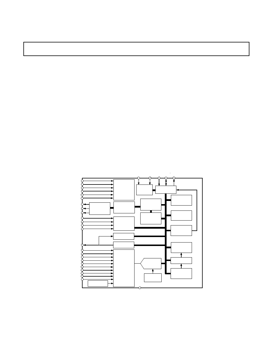
FUNCTIONAL BLOCK DIAGRAM
BAND GAP
REFERENCE
10-BIT
ADC
INPUT
SIGNAL
CONDITIONING
AND
ANALOG
MULTIPLEXER
GND
SERIAL BUS
INTERFACE
SCL
SDA
ADDRESS
POINTER
REGISTER
ADT7463
VALUE AND
LIMIT
REGISTERS
LIMIT
COMPARATORS
PWM
CONFIGURATION
REGISTERS
INTERRUPT
STATUS
REGISTERS
BAND GAP
TEMP. SENSOR
V
CC
TO ADT7463
INTERRUPT
MASKING
SMBALERT
V
CC
SMBUS
ADDRESS
SELECTION
ADDR EN
ADDR
SELECT
THERMAL
PROTECTION
PERFORMANCE
MONITORING
THERM
PWM
REGISTERS
AND
CONTROLLERS
PWM1
PWM2
PWM3
ACOUSTIC
ENHANCEMENT
CONTROL
AUTOMATIC
FAN SPEED
CONTROL
DYNAMIC
T
MIN
CONTROL
FAN SPEED
COUNTER
TACH1
TACH2
TACH3
TACH4
D1+
D1
D2+
D2
V
CC
+5V
IN
+12V
IN
+2.5V
IN
V
CCP
VID
REGISTER
VID5
VID4
VID3
VID2
VID1
VID0
GENERAL DESCRIPTION
The ADT7463 dBCOOL controller is a complete systems
monitor and multiple PWM fan controller for noise-sensitive
applications requiring active system cooling. It can monitor
12 V, 5 V, and 2.5 V CPU supply voltages, plus its own supply
voltage. It can monitor the temperature of up to two remote
sensor diodes, plus its own internal temperature. It can mea-
sure and control the speed of up to four fans so that they
operate at the lowest possible speed for minimum acoustic
noise. The Automatic Fan Speed Control Loop optimizes fan
speed for a given temperature. A unique Dynamic T
MIN
Con-
trol Mode enables the system thermals/acoustics to be
intelligently managed. The effectiveness of the system's thermal
solution can be monitored using the
THERM input. The
ADT7463 also provides critical Thermal Protection to the
system using the bidirectional
THERM pin as an output to
prevent system or component overheating.
*Protected by U.S. Patent Nos. 6,188,189; 6,169,442; 6,097,239; 5,982,221; and 5,867,012. Other patents pending.
dBCOOL is a trademark of Analog Devices, Inc.
Intel and Pentium are registered trademarks of Intel Corp.

REV. 0
2
ADT7463SPECIFICATIONS
1, 2, 3, 4
(T
A
= T
MIN
to T
MAX
, V
CC
= V
MIN
to V
MAX
, unless otherwise noted.)
Parameter
Min
Typ
Max
Unit
Test Conditions/Comments
POWER SUPPLY
Supply Voltage
3.0
5.0
5.5
V
Supply Current, I
CC
3
mA
Interface Inactive, ADC Active
20
µA
Standby Mode
TEMPERATURE-TO-DIGITAL CONVERTER
Local Sensor Accuracy
±0.5
±1.5
C
0 C T
A
70 C
±3
C
40 C T
A
+120 C
Resolution
0.25
C
Remote Diode Sensor Accuracy
±0.5
±1.5
C
0 C T
A
70 C; 0 C T
D
120 C
±2.5
C
0 C T
A
105 C; 0 C T
D
120 C
±3
C
0 C T
A
120 C; 0 C T
D
120 C
Resolution
0.25
C
Remote Sensor Source Current
180
µA
High Level
11
µA
Low Level
ANALOG-TO-DIGITAL CONVERTER
(INCLUDING MUX AND ATTENUATORS)
Total Unadjusted Error, TUE
±1.5
%
Differential Nonlinearity, DNL
±1
LSB
Power Supply Sensitivity
±0.1
%/V
Conversion Time (Voltage Input)
11.38
13
ms
Averaging Enabled
Conversion Time (Local Temperature)
12.09
13.5
ms
Averaging Enabled
Conversion Time (Remote Temperature)
25.59
28
ms
Averaging Enabled
Total Monitoring Cycle Time
120.17
134.5
ms
Averaging Enabled
Total Monitoring Cycle Time
13.51
15
ms
Averaging Disabled
Input Resistance
100
140
200
k
FAN RPM-TO-DIGITAL CONVERTER
Accuracy
±7
%
0 C T
A
70 C
±11
%
0 C T
A
105 C
±13
%
40 C T
A
+120 C
Full-Scale Count
65,535
Nominal Input RPM
109
RPM
Fan Count = 0xBFFF
329
RPM
Fan Count = 0x3FFF
5000
RPM
Fan Count = 0x0438
10000
RPM
Fan Count = 0x021C
Internal Clock Frequency
82.8
90
97.2
kHz
OPEN-DRAIN DIGITAL OUTPUTS,
PWM1PWM3, XTO
Current Sink, I
OL
8.0
mA
Output Low Voltage, V
OL
0.4
V
I
OUT
= 8.0 mA, V
CC
= 3.3 V
High Level Output Current, I
OH
0.1
1
µA
V
OUT
= V
CC
OPEN-DRAIN SERIAL DATA
BUS OUTPUT (SDA)
Output Low Voltage, V
OL
0.4
V
I
OUT
= 4.0 mA, V
CC
= 3.3 V
High Level Output Current, I
OH
0.1
1
µA
V
OUT
= V
CC
SMBUS DIGITAL INPUTS
(SCL, SDA)
Input High Voltage, V
IH
2.0
V
Input Low Voltage, V
IL
0.4
V
Hysteresis
500
mV
DIGITAL INPUT LOGIC LEVELS
(VID05)
Input High Voltage, V
IH
1.7
V
Bit 6 (THLD) Reg. 0x43 = 0
Input Low Voltage, V
IL
0.8
V
(VID Threshold = 1 V)
Input High Voltage, V
IH
0.8
V
Bit 6 (THLD) Reg. 0x43 = 1
Input Low Voltage, V
IL
0.4
V
(VID Threshold = 0.6 V)
REV. 0
ADT7463
3
Parameter
Min
Typ
Max
Unit
Test Conditions/Comment
DIGITAL INPUT LOGIC LEVELS
(TACH INPUTS)
Input High Voltage, V
IH
2.0
V
5.5
V
Maximum Input Voltage
Input Low Voltage, V
IL
+0.8
V
0.3
V
Minimum Input Voltage
Hysteresis
0.5
V p-p
DIGITAL INPUT LOGIC LEVELS
(THERM) AGTL+
Input High Voltage, V
IH
0.75 V
CCP
V
Input Low Voltage, V
IL
0.4
V
DIGITAL INPUT CURRENT
Input High Current, I
IH
1
µA
V
IN
= V
CC
Input Low Current, I
IL
+1
µA
V
IN
= 0
Input Capacitance, C
IN
5
pF
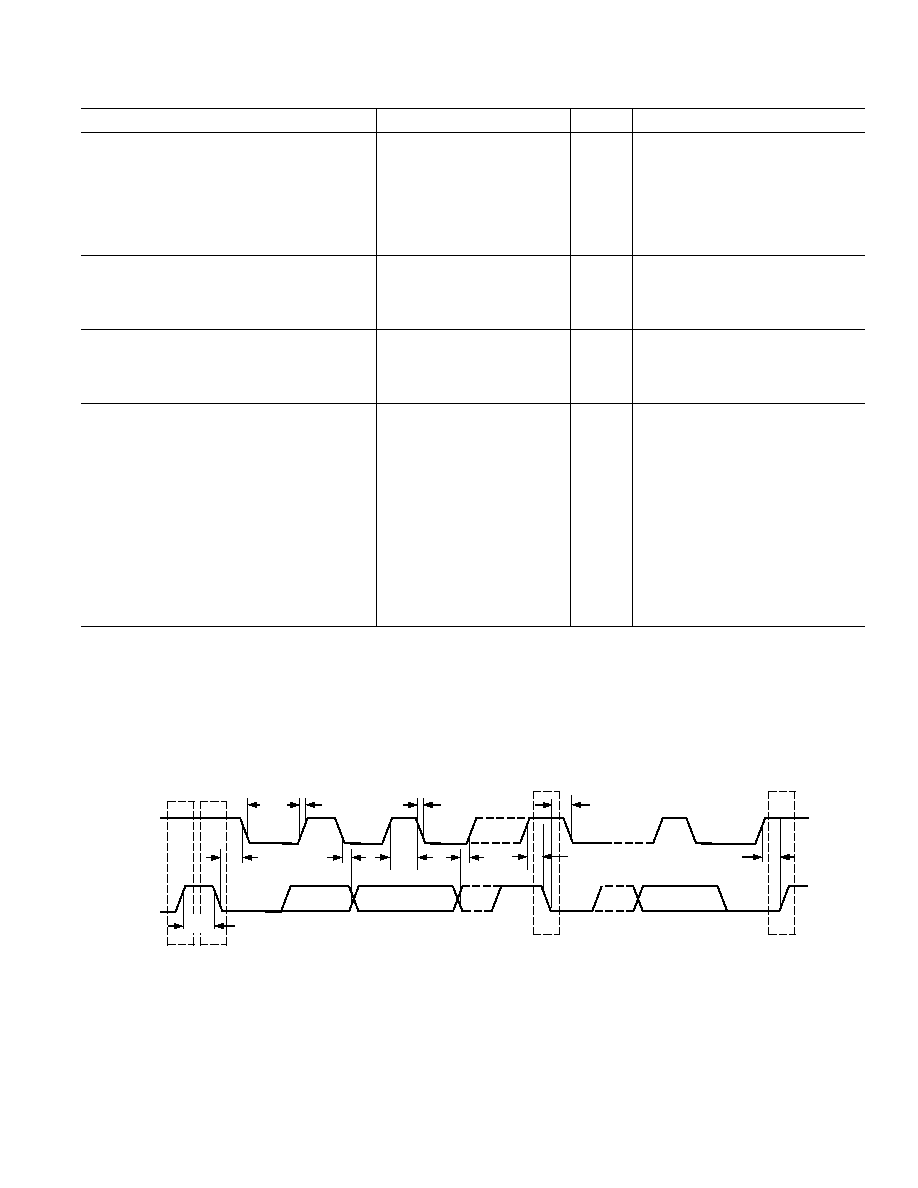
SERIAL BUS TIMING
Clock Frequency, f
SCLK
10
100
kHz
See Figure 1
Glitch Immunity, t
SW
50
ns
See Figure 1
Bus Free Time, t
BUF
4.7
µs
See Figure 1
Start Setup Time, t
SU;STA
4.7
µs
See Figure 1
Start Hold Time, t
HD;STA
4.0
µs
See Figure 1
SCL Low Time, t
LOW
4.7
µs
See Figure 1
SCL High Time, t
HIGH
4.0
50
µs
See Figure 1
SCL, SDA Rise Time, t
R
1000
ns
See Figure 1
SCL, SDA Fall Time, t
F
300
µs
See Figure 1
Data Setup Time, t
SU;DAT
250
ns
See Figure 1
Data Hold Time, t
HD;DAT
300
ns
See Figure 1
Detect Clock Low Timeout, t
TIMEOUT
15
35
ms
Can be optionally disabled
NOTES
1
All voltages are measured with respect to GND, unless otherwise specified.
2
Typicals are at T
A
= 25
°C and represent the most likely parametric norm.
3
Logic inputs will accept input high voltages up to V
MAX
even when the device is operating down to V
MIN
.
4
Timing specifications are tested at logic levels of V
IL
= 0.8 V for a falling edge and V
IH
= 2.0 V for a rising edge.
Specifications subject to change without notice.
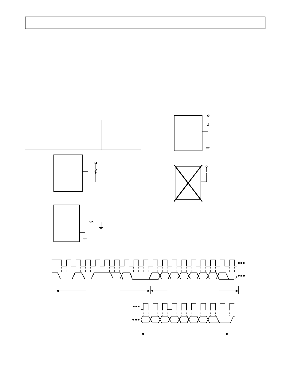
P
S
t
SU;DAT
t
HIGH
t
F
t
HD;DAT
t
R
t
LOW
t
SU;STO
P
S
SCL
SDA
t
HD;STA
t
HD;STA
t
SU;STA
t
BUF
Figure 1. Diagram for Serial Bus Timing

REV. 0
4
ADT7463
ABSOLUTE MAXIMUM RATINGS
*
Positive Supply Voltage (V
CC
) . . . . . . . . . . . . . . . . . . . . . 6.5 V
Voltage on 12 V
IN
Pin . . . . . . . . . . . . . . . . . . . . . . . . . . . 20 V
Voltage on Any Other Input or Output Pin . . . . 0.3 V to +6.5 V
Input Current at Any Pin . . . . . . . . . . . . . . . . . . . . . . .
±5 mA
Package Input Current . . . . . . . . . . . . . . . . . . . . . . .
±20 mA
Maximum Junction Temperature (T
J
max) . . . . . . . . . . 150
°C
Storage Temperature Range . . . . . . . . . . . . 65
°C to +150°C
Lead Temperature, Soldering
IR Reflow Peak Temperature . . . . . . . . . . . . . . . . . . . 220
°C
Lead Temperature (soldering 10 sec) . . . . . . . . . . . . . 300
°C
ESD Rating . . . . . . . . . . . . . . . . . . . . . . . . . . . . . . . . . 1500 V
*Stresses above those listed under Absolute Maximum Ratings may cause perma-
nent damage to the device. This is a stress rating only; functional operation of the
device at these or any other conditions above those indicated in the operational
section of this specification is not implied. Exposure to absolute maximum rating
conditions for extended periods may affect device reliability.
THERMAL CHARACTERISTICS
24-Lead QSOP Package:
JA
= 105
°C/W,
JC
= 39
°C/W
CAUTION
ESD (electrostatic discharge) sensitive device. Electrostatic charges as high as 4000 V readily
accumulate on the human body and test equipment and can discharge without detection. Although the
ADT7463 features proprietary ESD protection circuitry, permanent damage may occur on devices
subjected to high energy electrostatic discharges. Therefore, proper ESD precautions are recommended
to avoid performance degradation or loss of functionality.
ORDERING GUIDE
Temperature
Package
Package
Model
Range
Description
Option
ADT7463ARQ 40 C to +120 C 24-Lead QSOP
RQ-24
PIN CONFIGURATION
TOP VIEW
(Not to Scale)
24
23
22
21
20
19
18
17
16
15
14
13
1
2
3
4
5
6
7
8
9
10
11
12
ADT7463
TACH2
TACH1
PWM2/
SMBALERT
TACH3
VID3
SDA
SCL
GND
V
CC
VID2
VID1
VID0
PWM3/
ADDRESS ENABLE
TACH4/ADDRESS SELECT/
THERM
D2
D2+
D1
PWM1/XTO
V
CCP
+2.5V
IN
/
SMBALERT
+12V
IN
/VID5
D1+
VID4
+5V
IN
/
THERM

REV. 0
ADT7463
5
PIN FUNCTION DESCRIPTIONS
Pin No. Mnemonic
Description
1
SDA
Digital I/O (Open Drain). SMBus bidirectional serial data. Requires SMBus.
2
SCL
Digital Input (Open Drain). SMBus serial clock input. Requires SMBus pull-up.
3
GND
Ground Pin for the ADT7463.
4
V
CC
Power Supply. Can be powered by 3.3 V standby if monitoring in low power states is required. V
CC
is also
monitored through this pin. The ADT7463 can also be powered from a 5 V supply. Setting Bit 7 of
Configuration Register 1 (Reg. 0x40) rescales the V
CC
input attenuators to correctly measure a 5 V supply.
5
VID0
Digital Input (Open Drain). Voltage supply readouts from CPU. This value is read into the VID register (Reg. 0x43).
6
VID1
Digital Input (Open Drain). Voltage supply readouts from CPU. This value is read into the VID register (Reg. 0x43).
7
VID2
Digital Input (Open Drain). Voltage supply readouts from CPU. This value is read into the VID register (Reg. 0x43).
8
VID3
Digital Input (Open Drain). Voltage supply readouts from CPU. This value is read in to the VID register (Reg. 0x43).
9
TACH3
Digital Input (Open Drain). Fan tachometer input to measure speed of Fan3. Can be reconfigured as an analog in-
put (AIN3) to measure the speed of 2-wire fans.
10
PWM2
Digital Output (Open Drain). Requires 10 k
typical pull-up. Pulsewidth modulated output to control FAN 2 speed.
SMBALERT
Digital Output (Open Drain). This pin may be reconfigured as an
SMBALERT interrupt output to signal
out-of-limit conditions.
11
TACH1
Digital Input (Open Drain). Fan tachometer input to measure speed of Fan 1. Can be reconfigured as an analog in-
put (AIN1) to measure the speed of 2-wire fans.
12
TACH2
Digital Input (Open Drain). Fan tachometer input to measure speed of Fan 2. Can be reconfigured as an analog in-
put (AIN2) to measure the speed of 2-wire fans.
13
PWM3
Digital I/O (Open Drain). Pulsewidth modulated output to control Fan 3/4 speed. Requires 10 k
typical pull-up.
ADDRESS
ENABLE
If pulled low on power-up, this places the ADT7463 into Address Select mode, and the state of Pin 14 will
determine the ADT7463's slave address.
14
TACH4
Digital Input (Open Drain). Fan tachometer input to measure speed of Fan 4. Can be reconfigured as an analog in-
put (AIN4) to measure the speed of 2-wire fans.
ADDRESS
SELECT
If in Address Select mode, this pin determines the SMBus device address.
THERM
Alternatively, the pin may be reconfigured as a bidirectional
THERM pin. Can be used to time and monitor
assertions on the
THERM input. For example, can be connected to the PROCHOT output of Intel's Pentium 4
processor or to the output of a trip point temperature sensor. Can be used as an output to signal overtemperature
conditions.
15
D2
Cathode Connection to Second Thermal Diode
16
D2+
Anode Connection to Second Thermal Diode
17
D1
Cathode Connection to First Thermal Diode
18
D1+
Anode Connection to First Thermal Diode
19
VID4
Digital Input (Open Drain). Voltage supply readouts from CPU. This value is read into the VID register
(Reg. 0x43).
20
+5V
IN
Analog Input. Monitors +5 V power supply.
THERM
Alternatively, this pin may be reconfigured as a bidirectional
THERM pin. Can be used to time and monitor assertions
on the
THERM input. For example, can be connected to the PROCHOT output of Intel's Pentium 4 processor or
to the output of a trip point temperature sensor. Can be used as an output to signal overtemperature conditions.
21
+12V
IN
Analog Input. Monitors +12 V power supply.
VID5
Digital Input (Open Drain). Voltage supply readouts from CPU. This value is read into the VID register
(Reg. 0x43). Supports VRM10 solutions.
22
+2.5V
IN
Analog Input. Monitors +2.5 V supply, typically a chipset voltage.
SMBALERT
Digital Output (Open Drain). This pin may be reconfigured as an
SMBALERT interrupt output to signal
out-of-limit conditions.
23
V
CCP
Analog Input. Monitors processor core voltage (0 V3 V).
24
PWM1/XTO
Digital Output (Open Drain). Pulsewidth modulated output to control Fan 1 speed. Requires 10 k
typical pull-up.
Also functions as the output from the XOR tree in XOR Test Mode.

REV. 0
6
ADT7463
FUNCTIONAL DESCRIPTION
General Description
The ADT7463 is a complete systems monitor and multiple fan
controller for any system requiring monitoring and cooling. The
device communicates with the system via a serial System
Management Bus. The serial bus controller has an optional
address line for device selection (Pin 14), a serial data line
for reading and writing addresses and data (Pin 1), and an input
line for the serial clock (Pin 2). All control and programming
functions of the ADT7463 are performed over the serial bus. In
addition, two of the pins can be reconfigured as an
SMBALERT
output to indicate out-of-limit conditions.
Measurement Inputs
The device has six measurement inputs, four for voltage and
two for temperature. It can also measure its own supply voltage
and can measure ambient temperature with its on-chip tempera-
ture sensor.
Pins 20 through 23 are analog inputs with on-chip attenuators,
configured to monitor 5 V, 12 V, 2.5 V, and the processor core
voltage (2.25 V input), respectively.
Power is supplied to the chip via Pin 4, and the system also
monitors V
CC
through this pin. In PCs, this pin is normally
connected to a 3.3 V standby supply. This pin can, however, be
connected to a 5 V supply and monitor it without overranging.
Remote temperature sensing is provided by the D1 and D2
inputs, to which diode-connected, external temperature-sensing
transistors such as a 2N3904 or CPU thermal diode may be
connected.
The ADC also accepts input from an on-chip band gap tem-
perature sensor that monitors system ambient temperature.
Sequential Measurement
When the ADT7463 monitoring sequence is started, it cycles
sequentially through the measurement of analog inputs and the
temperature sensors. Measured values from these inputs are
stored in Value registers. These can be read out over the serial
bus, or can be compared with programmed limits stored in the
Limit registers. The results of out-of-limit comparisons are
stored in the Status registers, which can be read over the serial
bus to flag out-of-limit conditions.
Processor Voltage ID
Five digital inputs (VID0 to VID5--Pins 5 to 8, 19, and 21)
read the processor Voltage ID code and store it in the VID
register, from which it can be read out by the management
system over the serial bus. The VID code monitoring function is
compatible with both VRM9.x and future VRM10 solutions.
Additionally, an
SMBALERT can be generated to flag a change
in VID code.
ADT7463 Address Selection
Pin 13 is the dual function PWM3/
ADDRESS ENABLE pin.
If Pin 13 is pulled low on power-up, the ADT7463 will read the
state of Pin 14 (TACH4/ADDRESS SELECT/
THERM
pin) to
determine the ADT7463's slave address. If Pin 13 is high on
power-up, then the ADT7463 will default to SMBus slave
address 0x2E. This function is described in more detail later.
INTERNAL REGISTERS OF THE ADT7463
A brief description of the ADT7463's principal internal registers
is given below. More detailed information on the function of
each register is given in Tables IV to XLII.
Configuration Registers
The Configuration registers provide control and configuration
of the ADT7463, including alternate pinout functionality.
Address Pointer Register
This register contains the address that selects one of the other
internal registers. When writing to the ADT7463, the first byte
of data is always a register address, which is written to the
Address Pointer Register.
Status Registers
These registers provide the status of each limit comparison and
are used to signal out-of-limit conditions on the temperature,
voltage, or fan speed channels. If Pin 10 or Pin 22 is con-
figured as
SMBALERT, then this pin will assert low whenever
a status bit gets set.
Interrupt Mask Registers
These registers allow each interrupt status event to be masked
when Pin 10 or Pin 22 is configured as an
SMBALERT
output.
VID Register
The status of the VID0 to VID5 pins of the processor can read
from this register. VID code changes can also generate
SMBALERT interrupts.
Value and Limit Registers
The results of analog voltage inputs, temperature, and fan
speed measurements are stored in these registers, along with
their limit values.
Offset Registers
These registers allow each temperature channel reading to be
offset by a twos complement value written to these registers.
T
MIN
Registers
These registers program the starting temperature for each fan
under Automatic Fan Speed Control.
T
RANGE
Registers
These registers program the temperature-to-fan speed control
slope in Automatic Fan Speed Control Mode for each PWM
output.
Operating Point Registers
These registers define the target operating temperatures for each
thermal zone when running under dynamic T
MIN
control. This
function allows the cooling solution to adjust dynamically in
response to measured temperature and system performance.
Enhance Acoustics Registers
These registers allow each PWM output controlling fan to be
tweaked to enhance the system's acoustics.
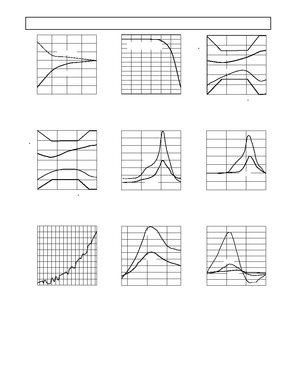
REV. 0
Typical Performance CharacteristicsADT7463
7
LEAKAGE RESISTANCE M
REMO
TE
TEMPERA
T
URE ERR
OR
C
15
10
20
1
3.3
100
10
30
0
5
10
15
5
DXP TO GND
DXP TO V
CC
(3.3V)
TPC 1. Temperature Error vs.
Leakage Resistance
TEMPERATURE C
TEMPERA
T
URE ERR
OR
C
3
40
10
110
60
1
0
2
1
3
2
LOW LIMIT
HIGH LIMIT
3 SIGMA
+3 SIGMA
TPC 4. Local Temperature Error vs.
Actual Temperature
1.9
1.8
1.8
1.7
1.7
1.6
1.6
1.5
1.5
1.4
1.4
2.5
2.6
3.0
3.4
3.8
4.2
4.6
5.0
5.4
5.5
SUPPLY VOLTAGE V
SUPPL
Y CURRENT mA
TPC 7. Supply Current vs.
Supply Voltage
DXPDXN CAPACITANCE nF
REMO
TE
TEMPERA
T
URE ERR
OR
C
3
1
0
3
6
9
12
15
18
21
24
27
2.2
3.3
4.7
10
22
47
30
33
36
REMOTE TEMPERATURE
ERROR ( C)
TPC 2. Temperature Error vs.
Capacitance between D+ and D
FREQUENCY Hz
REMO
TE
TEMPERA
T
URE
C
14
12
2
100k
550k
50M
5M
6
4
0
2
10
8
100mV
250mV
TPC 5. Remote Temperature Error
vs. Power Supply Noise Frequency
FREQUENCY Hz
REMO
TE
TEMPERA
T
URE ERR
OR
C
16
60k
14
12
10
8
6
4
2
0
2
110k
1M
10M
50M
10mV
20mV
TPC 8. Remote Temperature Error
vs. Differential Mode Noise
Frequency
TEMPERATURE C
TEMPERA
T
URE ERR
OR
C
3
40
2
1
0
1
2
3
10
60
110
3 SIGMA
+3 SIGMA
LOW LIMIT
HIGH LIMIT
TPC 3. Remote Temperature Error
vs. Actual Temperature
FREQUENCY Hz
LOCAL
TEMPERA
T
URE ERR
OR
C
12.5
10.0
5.0
100k
550k
50M
5M
5.0
2.5
2.5
0
7.5
100mV
250mV
TPC 6. Local Temperature Error vs.
Power Supply Noise Frequency
FREQUENCY Hz
REMO
TE
TEMPERA
T
URE ERR
OR
C
40
10k
35
30
25
20
15
10
5
0
5
10
100k
1M
10M
20mV
40mV
100mV
TPC 9. Remote Temperature Error
vs. Common-Mode Noise
Frequency
REV. 0
8
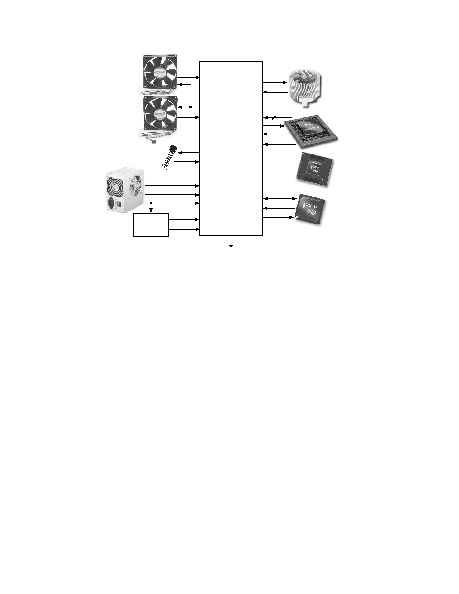
ADT7463
TACH2
PWM3
TACH3
D1+
D1
3.3VSB
5V
12V/VID5
CURRENT
V
CORE
GND
SMBALERT
ADT7463
SCL
SDA
THERM
D2+
D2
VID[0:4]/VID[0:5]
TACH1
PWM1
ADP316x
VRM
CONTROLLER
FRONT
CHASSIS
FAN
REAR
CHASSIS
FAN
AMBIENT
TEMPERATURE
V
COMP
5(VRM9)/6(VRM10)
PROCHOT
Figure 2. Recommended Implementation
RECOMMENDED IMPLEMENTATION
Configuring the ADT7463 as in Figure 2 allows the systems
designer the following features:
· Six VID inputs (VID0 to VID5) for VRM10 support
· Two PWM outputs for fan control of up to three fans (the
front and rear chassis fans are connected in parallel)
· Three TACH fan speed measurement inputs
· VCC measured internally through Pin 4
· CPU core voltage measurement (V
CORE
)
· 2.5 V measurement input used to monitor CPU current
(connected to V
COMP
output of ADP316x VRM Control-
ler). This is used to determine CPU power consumption.
· 5 V measurement input
· VRM temperature uses local temperature sensor
· CPU temperature measured using Remote 1 temperature
channel
· Ambient temperature measured through Remote 2 tempera-
ture channel
· If not using VID5, this pin can be reconfigured as the 12 V
monitoring input
· Bidirectional THERM pin. Allows Intel P4 PROCHOT
Monitoring and can function as an overtemperature
THERM output.
· SMBALERT system interrupt output
See ADT7463 Configuration App Note for more information
and register settings for all possible configurations.
REV. 0
ADT7463
9
SERIAL BUS INTERFACE
Control of the ADT7463 is carried out using the serial System
Management bus (SMBus). The ADT7463 is connected to this
bus as a slave device, under the control of a master controller.
The ADT7463 has a 7-bit serial bus address. When the device
is powered up with Pin 13 (PWM3/
Address Enable) high, the
ADT7463 will have a default SMBus address of 0101110 or
0x5C. If more than one ADT7463 is to be used in a system,
then each ADT7463 should be placed in Address Select Mode
by strapping Pin 13 low on power-up. The logic state of Pin 14
then determines the device's SMBus address.
The device address is sampled and latched on the first valid
SMBus transaction, so any attempted addressing changes made
thereafter will have no immediate effect.
Table I. Address Select Mode
Pin 13 State
Pin 14 State
Address
0
Low (10 k
to GND)
0101100 (0x2C)
0
High (10 k
pull-up)
0101101 (0x2D)
1
Don't Care
0101110 (0x2E)
(default)
ADT7463
14
13
ADDR_SEL
PWM3/
ADDR_EN
V
CC
10k
ADDRESS = 0x2E
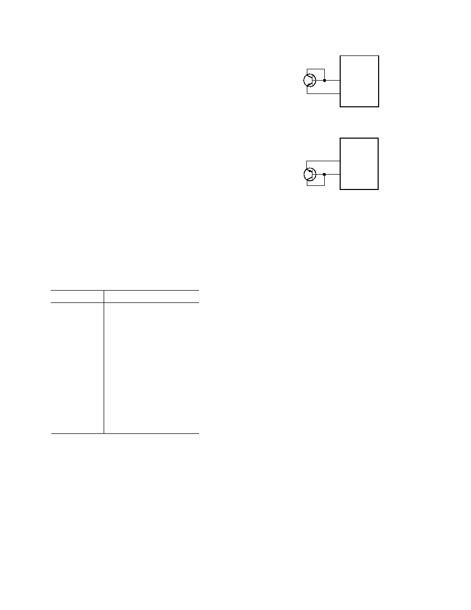
Figure 3. Default SMBus Address = 0x2E
ADT7463
14
13
ADDR_SEL
PWM3/
ADDR_EN
10k
ADDRESS = 0x2C
Figure 4. SMBus Address = 0x2C (Pin 14 = 0)
The ability to make hardwired changes to the SMBus slave
address allows the user to avoid conflicts with other devices
sharing the same serial bus, for example, if more than one
ADT7463 is used in a system.
The serial bus protocol operates as follows:
1. The master initiates data transfer by establishing a START
condition, defined as a high to low transition on the serial
data line SDA while the serial clock line SCL remains high.
This indicates that an address/data stream will follow. All
slave peripherals connected to the serial bus respond to the
START condition and shift in the next eight bits, consisting
of a 7-bit address (MSB first) plus a R/
W bit, which deter-
mines the direction of the data transfer, i.e., whether data
will be written to or read from the slave device.
ADT7463
ADDR_SEL
PWM3/
ADDR_EN
ADDRESS = 0x2D
14
13
V
CC
10k
Figure 5. SMBus Address = 0x2D (Pin 14 = 1)
ADT7463
14
13
ADDR_SEL
PWM3/
ADDR_EN
V
CC
10k
DO NOT LEAVE ADDR_EN
UNCONNECTED! CAN
CAUSE UNPREDICTABLE
ADDRESSES
NC
CARE SHOULD BE TAKEN TO ENSURE THAT PIN 13
(PWM3/
ADDR_EN) IS EITHER TIED HIGH OR LOW. LEAVING PIN 13
FLOATING COULD CAUSE THE ADT7463 TO POWER UP WITH AN
UNEXPECTED ADDRESS.
NOTE THAT IF THE ADT7463 IS PLACED INTO ADDRESS SELECT
MODE, PINS 13 AND 14 CANNOT BE USED AS THE ALTERNATE
FUNCTIONS (PWM3, TACH4/
THERM) ONLY IF THE CORRECT
CIRCUIT IS MUXED IN AT THE CORRECT TIME
Figure 6. Unpredictable SMBus Address if Pin 13
is Unconnected
R/
W
0
SCL
SDA
1
0
1
1
A1
A0
D7
D6
D5
D4
D3
D2
D1
D0
ACK. BY
ADT7463
START BY
MASTER
FRAME 1
SERIAL BUS ADDRESS
BYTE
FRAME 2
ADDRESS POINTER REGISTER BYTE
1
9
1
ACK. BY
ADT7463
9
D7
D6
D5
D4
D3
D2
D1
D0
ACK. BY
ADT7463
STOP BY
MASTER
FRAME 3
DATA
BYTE
1
9
SCL (CONTINUED)
SDA (CONTINUED)
Figure 7. Writing a Register Address to the Address Pointer Register, Then Writing Data to the Selected Register
REV. 0
10
ADT7463
The peripheral whose address corresponds to the transmitted
address responds by pulling the data line low during the low
period before the ninth clock pulse, known as the Acknowl-
edge Bit. All other devices on the bus now remain idle while
the selected device waits for data to be read from or written
to it. If the R/
W bit is a 0, then the master will write to the
slave device. If the R/
W bit is a 1, the master will read from
the slave device.
2. Data is sent over the serial bus in sequences of nine clock
pulses, eight bits of data followed by an Acknowledge Bit
from the slave device. Transitions on the data line must
occur during the low period of the clock signal and remain
stable during the high period, as a low to high transition
when the clock is high may be interpreted as a STOP signal.
The number of data bytes that can be transmitted over the
serial bus in a single READ or WRITE operation is limited
only by what the master and slave devices can handle.
3. When all data bytes have been read or written, stop condi-
tions are established. In WRITE mode, the master will pull
the data line high during the tenth clock pulse to assert a
STOP condition. In READ mode, the master device will
override the acknowledge bit by pulling the data line high
during the low period before the ninth clock pulse. This is
known as No Acknowledge. The master will then take the
data line low during the low period before the tenth clock
pulse, and then high during the tenth clock pulse to assert a
STOP condition.
Any number of bytes of data can be transferred over the serial
bus in one operation, but it is not possible to mix read and write
in one operation because the type of operation is determined at
the beginning and cannot subsequently be changed without
starting a new operation.
In the case of the ADT7463, write operations contain either one
or two bytes, and read operations contain one byte and perform
the following functions:
To write data to one of the device data registers or read data
from it, the Address Pointer Register must be set so that the
correct data register is addressed, then data can be written into
that register or read from it. The first byte of a write operation
always contains an address that is stored in the Address Pointer
Register. If data is to be written to the device, then the write
operation contains a second data byte that is written to the
register selected by the Address Pointer Register.
This is illustrated in Figure 7. The device address is sent over
the bus followed by R/
W being set to 0. This is followed by two
data bytes. The first data byte is the address of the internal data
register to be written to, which is stored in the Address Pointer
Register. The second data byte is the data to be written to the
internal data register.
When reading data from a register, there are two possibilities:
1. If the ADT7463's Address Pointer Register value is un-
known or not the desired value, it is first necessary to set it to
the correct value before data can be read from the desired
data register. This is done by performing a write to the
ADT7463 as before, but only the data byte containing the
register address is sent as data is not to be written to the
register. This is shown in Figure 8.
A read operation is then performed consisting of the serial
bus address, R/
W bit set to 1, followed by the data byte read
from the data register. This is shown in Figure 9.
2. If the Address Pointer Register is known to be already at the
desired address, data can be read from the corresponding
data register without first writing to the Address Pointer
Register, so Figure 8 can be omitted.
Notes
1. It is possible to read a data byte from a data register without
first writing to the Address Pointer Register if the Address
Pointer Register is already at the correct value. However, it is
not possible to write data to a register without writing to the
Address Pointer Register because the first data byte of a
write is always written to the Address Pointer Register.
2. In Figures 7 to 9, the serial bus address is shown as the de-
fault value 01011(A1)(A0), where A1 and A0 are set by the
Address Select Mode function previously defined.
3. In addition to supporting the Send Byte and Receive Byte
protocols, the ADT7463 also supports the Read Byte proto-
col (see System Management Bus specifications Rev. 2.0 for
more information).
R/
W
0
SCL
SDA
1
0
1
1
A1
A0
D7
D6
D5
D4
D3
D2
D1
D0
ACK. BY
ADT7463
STOP BY
MASTER
START BY
MASTER
FRAME 1
SERIAL BUS ADDRESS
BYTE
FRAME 2
ADDRESS POINTER REGISTER BYTE
1
9
1
ACK. BY
ADT7463
9
Figure 8. Writing to the Address Pointer Register Only
R/
W
0
SCL
SDA
1
0
1
1
A1
A0
D7
D6
D5
D4
D3
D2
D1
D0
NO ACK. BY
MASTER
STOP BY
MASTER
START BY
MASTER
FRAME 1
SERIAL BUS ADDRESS
BYTE
FRAME 2
DATA BYTE FROM ADT7463
1
9
1
ACK. BY
ADT7463
9
Figure 9. Reading Data from a Previously Selected Register

REV. 0
ADT7463
11
4. If it is required to perform several read or write operations in
succession, the master can send a repeat start condition
instead of a stop condition to begin a new operation.
ADT7463 WRITE OPERATIONS
The SMBus specification defines several protocols for different
types of read and write operations. The ones used in the
ADT7463 are discussed below. The following abbreviations are
used in the diagrams:
S START
P STOP
R READ
W WRITE
A ACKNOWLEDGE
A NO ACKNOWLEDGE
The ADT7463 uses the following SMBus write protocols:
Send Byte
In this operation, the master device sends a single command
byte to a slave device as follows:
1. The master device asserts a start condition on SDA.
2. The master sends the 7-bit slave address followed by the
write bit (low).
3. The addressed slave device asserts ACK on SDA.
4. The master sends a command code.
5. The slave asserts ACK on SDA.
6. The master asserts a STOP condition on SDA and the
transaction ends.
For the ADT7463, the send byte protocol is used to write a
register address to RAM for a subsequent single byte read from
the same address. This is illustrated in Figure 10.
S
SLAVE
ADDRESS
W A
A P
1
2
3
4
5
6
REGISTER
ADDRESS
Figure 10. Setting a Register Address for Subsequent Read
If it is required to read data from the register immediately after
setting up the address, the master can assert a repeat start con-
dition immediately after the final ACK and carry out a single
byte read without asserting an intermediate stop condition.
Write Byte
In this operation, the master device sends a command byte and
one data byte to the slave device as follows:
1. The master device asserts a start condition on SDA.
2. The master sends the 7-bit slave address followed by the
write bit (low).
3. The addressed slave device asserts ACK on SDA.
4. The master sends a command code.
5. The slave asserts ACK on SDA.
6. The master sends a data byte.
7. The slave asserts ACK on SDA.
8. The master asserts a STOP condition on SDA to end the
transaction.
This is illustrated in Figure 11.
S
SLAVE
ADDRESS
W A
1
2
3
4
5
6
A DATA A P
7 8
REGISTER
ADDRESS
Figure 11. Single Byte Write to a Register
ADT7463 READ OPERATIONS
The ADT7463 uses the following SMBus read protocols:
Receive Byte
This is useful when repeatedly reading a single register. The
register address needs to have been set up previously. In this
operation, the master device receives a single byte from a slave
device as follows:
1. The master device asserts a START condition on SDA.
2. The master sends the 7-bit slave address followed by the
read bit (high).
3. The addressed slave device asserts ACK on SDA.
4. The master receives a data byte.
5. The master asserts NO ACK on SDA.
6. The master asserts a STOP condition on SDA and the trans-
action ends.
In the ADT7463, the receive byte protocol is used to read a
single byte of data from a register whose address has previously
been set by a send byte or write byte operation.
S
SLAVE
ADDRESS
R
A DATA
A P
1
2
3
4
5
6
Figure 12. Single Byte Read from a Register
ALERT RESPONSE ADDRESS
Alert Response Address (ARA) is a feature of SMBus devices
that allows an interrupting device to identify itself to the host
when multiple devices exist on the same bus.
The
SMBALERT output can be used as an interrupt output or
can be used as an
SMBALERT. One or more outputs can be
connected to a common
SMBALERT line connected to the
master. If a device's
SMBALERT line goes low, the following
procedure occurs:
1.
SMBALERT is pulled low.
2. Master initiates a read operation and sends the Alert
Response Address (ARA = 0001 100). This is a general
call address that must not be used as a specific device
address.
3. The device whose
SMBALERT output is low responds to
the Alert Response Address, and the master reads its device
address. The address of the device is now known and it can
be interrogated in the usual way.
4. If more than one device's
SMBALERT output is low, the
one with the lowest device address will have priority in accor-
dance with normal SMBus arbitration.
5. Once the ADT7463 has responded to the Alert Response
Address, the master must read the Status Registers and the
SMBALERT will only be cleared if the error condition has
gone away.
SMBUS TIMEOUT
The ADT7463 includes an SMBus Timeout feature. If there is
no SMBus activity for 35 ms, the ADT7463 assumes that the bus
is locked and releases the bus. This prevents the device from
locking or holding the SMBus expecting data. Some SMBus
controllers cannot handle the SMBus Timeout feature, so it
can be disabled.
CONFIGURATION REGISTER 1 Register 0x40
<6> TODIS = 0; SMBus Timeout ENABLED (default)
<6> TODIS = 1; SMBus Timeout DISABLED
REV. 0
12
ADT7463
VOLTAGE MEASUREMENT INPUTS
The ADT7463 has four external voltage measurement channels.
It can also measure its own supply voltage, V
CC
.
Pins 20 to 23 are dedicated to measuring 5 V, 12 V, and 2.5 V
supplies and the processor core voltage V
CCP
(0 V to 3 V input).
The V
CC
supply voltage measurement is carried out through the
V
CC
pin (Pin 4). Setting Bit 7 of Configuration Register 1 (Reg.
0x40) allows a 5 V supply to power the ADT7463 and be mea-
sured without overranging the V
CC
measurement channel. The
2.5 V input can be used to monitor a chipset supply voltage in
computer systems.
ANALOG-TO-DIGITAL CONVERTER
All analog inputs are multiplexed into the on-chip, successive-
approximation, analog-to-digital converter. This has a resolu-
tion of 10 bits. The basic input range is 0 V to 2.25 V, but the
inputs have built-in attenuators to allow measurement of 2.5 V,
3.3 V, 5 V, 12 V and the processor core voltage V
CCP
without
any external components. To allow for the tolerance of these
supply voltages, the ADC produces an output of 3/4 full scale
(decimal 768 or 300 hex) for the nominal input voltage, and so
has adequate headroom to cope with overvoltages.
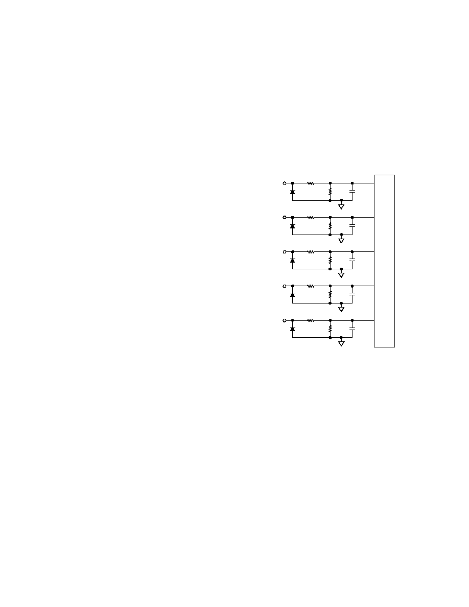
INPUT CIRCUITRY
The internal structure for the analog inputs is shown in Figure 13.
Each input circuit consists of an input protection diode, an attenu-
ator, plus a capacitor to form a first-order low-pass filter that gives
the input immunity to high frequency noise.
VOLTAGE MEASUREMENT REGISTERS
Reg. 0x20 2.5 V Reading = 0x00 default
Reg. 0x21 V
CCP
Reading = 0x00 default
Reg. 0x22 V
CC
Reading = 0x00 default
Reg. 0x23 5 V Reading = 0x00 default
Reg. 0x24 12 V Reading = 0x00 default
VOLTAGE MEASUREMENT LIMIT REGISTERS
Associated with each voltage measurement channel are high and
low limit registers. Exceeding the programmed high or low limit
causes the appropriate Status bit to be set. Exceeding either
limit can also generate
SMBALERT interrupts.
Reg. 0x44 2.5 V Low Limit = 0x00 default
Reg. 0x45 2.5 V High Limit = 0xFF default
Reg. 0x46 V
CCP
Low Limit = 0x00 default
Reg. 0x47 V
CCP
High Limit = 0xFF default
Reg. 0x48 V
CC
Low Limit = 0x00 default
Reg. 0x49 V
CC
High Limit = 0xFF default
Reg. 0x4A 5 V Low Limit = 0x00 default
Reg. 0x4B 5 V High Limit = 0xFF default
Reg. 0x4C 12 V Low Limit = 0x00 default
Reg. 0x4D 12 V High Limit = 0xFF default
30pF
120k
30pF
93k
MUX
30pF
68k
30pF
45k
52.5k
35pF
17.5k
94k
71k
47k
20k
12V
IN
5V
IN
3.3V
IN
2.5V
IN
V
CCPIN
Figure 13. Structure of Analog Inputs
Table II shows the input ranges of the analog inputs and output
codes of the 10-bit ADC.
When the ADC is running, it samples and converts a voltage
input in 711
µs and averages 16 conversions to reduce noise; a
measurement on each input takes nominally 11.38 ms.

REV. 0
ADT7463
13
Table II. 10-Bit A/D Output Code vs. V
IN
Input Voltage
A/D Output
+12V
IN
+5V
IN
V
CC
(3.3V
IN
)
*
+2.5V
IN
+V
CCPIN
Decimal
Binary (10 Bits)
<0.0156
<0.0065
<0.0042
<0.0032
<0.00293
0
00000000 00
0.01560.0312
0.00650.0130
0.00420.0085
0.00320.0065
0.02930.0058
1
00000000 01
0.03120.0469
0.01300.0195
0.00850.0128
0.00650.0097
0.00580.0087
2
00000000 10
0.04690.0625
0.01950.0260
0.01280.0171
0.00970.0130
0.00870.0117
3
00000000 11
0.06250.0781
0.02600.0325
0.01710.0214
0.01300.0162
0.01170.0146
4
00000001 00
0.07810.0937
0.03250.0390
0.02140.0257
0.01620.0195
0.01460.0175
5
00000001 01
0.09370.1093
0.03900.0455
0.02570.0300
0.01950.0227
0.01750.0205
6
00000001 10
0.10930.1250
0.04550.0521
0.03000.0343
0.02270.0260
0.02050.0234
7
00000001 11
0.12500.14060
0.05210.0586
0.03430.0386
0.02600.0292
0.02340.0263
8
00000010 00
·
·
·
4.00004.0156
1.66751.6740
1.10001.1042
0.83250.8357
0.75000.7529
256 (1/4 scale)
01000000 00
·
·
·
8.00008.0156
3.33003.3415
2.20002.2042
1.66501.6682
1.50001.5029
512 (1/2 scale)
10000000 00
·
·
·
12.000012.0156
5.00255.0090
3.30003.3042
2.49752.5007
2.25002.2529
768 (3/4 scale) 11000000 00
·
·
·
15.828115.8437
6.59836.6048
4.35274.3570
3.29423.2974
2.96772.9707
1013
11111101 01
15.843715.8593
6.60486.6113
4.35704.3613
3.29743.3007
2.97072.9736
1014
11111101 10
15.859315.8750
6.61136.6178
4.36134.3656
3.30073.3039
2.97362.9765
1015
11111101 11
15.875015.8906
6.61786.6244
4.36564.3699
3.30393.3072
2.97652.9794
1016
11111110 00
15.890615.9062
6.62446.6309
4.36994.3742
3.30723.3104
2.97942.9824
1017
11111110 01
15.906215.9218
6.63096.6374
4.37424.3785
3.31043.3137
2.98242.9853
1018
11111110 10
15.921815.9375
6.63746.4390
4.37854.3828
3.31373.3169
2.98532.9882
1019
11111110 11
15.937515.9531
6.64396.6504
4.38284.3871
3.31693.3202
2.98822.9912
1020
11111111 00
15.953115.9687
6.65046.6569
4.38714.3914
3.32023.3234
2.99122.9941
1021
11111111 01
15.968715.9843
6.65696.6634
4.39144.3957
3.32343.3267
2.99412.9970
1022
11111111 10
>15.9843
>6.6634
>4.3957
>3.3267
>2.9970
1023
11111111 11
*The V
CC
output codes listed assume that V
CC
is 3.3 V. If V
CC
input is reconfigured for 5 V operation (by setting Bit 7 of Configuration Register 1), then the V
CC
output codes are the same as for the 5 V
IN
column.

REV. 0
14
ADT7463
VIC CODE MONITORING
The ADT7463 has five dedicated Voltage ID (VID Code)
inputs. These are digital inputs that can be read back through
the VID Register (Reg. 0x43) to determine the Processor Volt-
age required/being used in the system. Five VID Code inputs
support VRM9.x solutions. In addition, Pin 21 (12 V input) can
be reconfigured as a sixth VID input to satisfy future VRM
requirements.
VID CODE REGISTER Register 0x43
<0> = VID0 (reflects logic state of Pin 5)
<1> = VID1 (reflects logic state of Pin 6)
<2> = VID2 (reflects logic state of Pin 7)
<3> = VID3 (reflects logic state of Pin 8)
<4> = VID4 (reflects logic state of Pin 19)
<5> = VID5 (Reconfigurable 12 V input). This bit reads 0
when Pin 21 is configured as the 12 V input. This bit reflects
the logic state of Pin 21 when the pin is configured as VID5.
VID CODE INPUT THRESHOLD VOLTAGE
The switching threshold for the VID Code inputs is approxi-
mately 1 V. To enable future compatibility, it is possible to
reduce the VID Code input threshold to 0.6 V. Bit 6
(THLD) of VID Register (Reg. 0x43) controls the VID input
threshold voltage.
VID CODE REGISTER Register 0x43
<6> THLD = 0; VID Switching Threshold = 1 V,
V
OL
< 0.8V, V
IH
> 1.7 V, V
MAX
= 3.3 V
THLD = 1; VID Switching Threshold = 0.6 V
V
OL
< 0.4 V, V
IH
> 0.8 V, V
MAX
= 3.3 V
RECONFIGURING PIN 21 (12V/VID5) AS VID5 INPUT
Pin 21 can be reconfigured as a sixth VID Code input (VID5)
for VRM10 compatible systems. Since the pin is configured as
VID5, it will no longer be possible to monitor a 12 V supply.
Bit 7 of the VID Register (Reg. 0x43) determines the function
of Pin 21. System or BIOS software can read the state of Bit 7
to determine whether the system is designed to monitor 12 V or
is monitoring a sixth VID input.
VID CODE REGISTER Register 0x43
<7> VIDSEL = 0; Pin 21 functions as 12 V measurement
input. Software can read this bit to determine that there are five
VID inputs being monitored. Bit 5 of Register 0x43 (VID5)
always reads back 0. Bit 0 of Status Register 2 (Reg. 0x42)
reflects 12 V out-of-limit measurements.
VIDSEL = 1; Pin 21 functions as the sixth VID Code input
(VID5). Software can read this bit to determine that there are
six VID inputs being monitored. Bit 5 of Register 0x43 reflects
the logic state of Pin 21. Bit 0 of Status Register 2 (Reg. 0x42)
reflects VID Code changes.
VID CODE CHANGE DETECT FUNCTION
The ADT7463 has a VID Code change detect function. When
Pin 21 is configured as the VID5 input, VID Code changes can
be detected and reported back by the ADT7463. Bit 0 of Status
Register 2 (Reg. 0x42) is the 12V/VC bit and denotes a VID
change when set. The VID Code Change bit gets set when the
logic states on the VID inputs are different than they were 11
µs
previously. The change of VID code can be used to generate
an
SMBALERT interrupt. If an SMBALERT interrupt is not
required, Bit 0 of Interrupt Mask Register 2 (Reg. 0x75)
when set, will prevent
SMBALERTs from occurring on VID
code changes.
STATUS REGISTER 2 Register 0x42
<0> 12V/VC = 0; If Pin 21 is configured as VID5, then a
logic 0 denotes no change in VID Code within last 11
µs.
<0> 12V/VC = 1; If Pin 21 is configured as VID5, then a logic
1 means that a change has occurred on the VID Code inputs
within the last 11
µs. An SMBALERT will be generated if this
function is enabled.
ADDITIONAL ADC FUNCTIONS
A number of other functions are available on the ADT7463 to
offer the systems designer increased flexibility:
Turn Off Averaging
For each voltage measurement read from a value register, 16
readings have actually been made internally and the results
averaged before being placed into the value register. There may
be an instance where you would like to speed up conversions.
Setting Bit 4 of Configuration Register 2 (Reg. 0x73) turns
averaging off. This effectively gives a reading 16 times faster
(711
µs) but the reading may be noisier.
Bypass Voltage Input Attenuators
Setting Bit 5 of Configuration Register 2 (Reg 0x73) removes
the attenuation circuitry from the 2.5 V, V
CCP
, V
CC
, 5 V, and
12 V inputs. This allows the user to directly connect external
sensors or rescale the analog voltage measurement inputs for
other applications. The input range of the ADC without the
attenuators is 0 V to 2.25 V.
Single-Channel ADC Conversion
Setting Bit 6 of Configuration Register 2 (Reg. 0x73) places the
ADT7463 into Single-Channel ADC Conversion Mode. In this
mode, the ADT7463 can be made to read a single voltage chan-
nel only. If the internal ADT7463 clock is used, the selected
input will be read every 711
µs. The appropriate ADC Channel
is selected by writing to Bits <7:5> of the TACH1 Minimum
High Byte Register (0x55).
Bits <7:5> Reg 0x55
Channel Selected
000
2.5 V
001
V
CCP
010
V
CC
011
5 V
100
12 V
Configuration Register 2 (Reg. 0x73)
<4> = 1 Averaging Off
<5> = 1 Bypass Input Attenuators
<6> = 1 Single-Channel Convert Mode
TACH1 Minimum High Byte (Reg. 0x55)
<7:5> Selects ADC Channel for Single-Channel Convert Mode
REV. 0
ADT7463
15
TEMPERATURE MEASUREMENT SYSTEM
Local Temperature Measurement
The ADT7463 contains an on-chip band gap temperature sensor
whose output is digitized by the on-chip 10-bit ADC. The 8-bit
MSB temperature data is stored in the Local Temp Register
(Address 26h). As both positive and negative temperatures can be
measured, the temperature data is stored in twos complement
format, as shown in Table III. Theoretically, the temperature sensor
and ADC can measure temperatures from 128 C to +127 C
with a resolution of 0.25 C. However, this exceeds the operating
temperature range of the device, so local temperature measure-
ments outside this range are not possible.
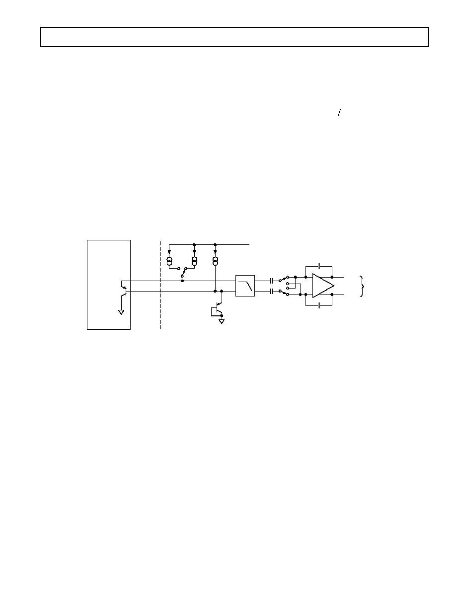
Remote Temperature Measurement
The ADT7463 can measure the temperature of two remote diode
sensors or diode-connected transistors connected to Pins 15 and
16, or 17 and 18.
The forward voltage of a diode or diode-connected transistor
operated at a constant current exhibits a negative temperature
coefficient of about 2 mV/ C. Unfortunately, the absolute
D+
D
REMOTE
SENSING
TRANSISTOR
I
N I
I
BIAS
V
DD
V
OUT+
TO ADC
V
OUT
BIAS
DIODE
LOW-PASS
FILTER
f
C
= 65kHz
THERMDA
THERMDC
CPU
Figure 14. Signal Conditioning for Remote Diode Temperature Sensors
value of V
BE
varies from device to device and individual calibra-
tion is required to null this out, so the technique is unsuitable
for mass production. The technique used in the ADT7463 is to
measure the change in V
BE
when the device is operated at two
different currents.
This is given by:
V
KT q
N
BE
=
× ln( )
where:
K is Boltzmann's constant
q is charge on the carrier
T is absolute temperature in Kelvins
N is ratio of the two currents.
Figure 14 shows the input signal conditioning used to measure
the output of a remote temperature sensor. This figure shows the
external sensor as a substrate transistor, provided for temperature
monitoring on some microprocessors. It could equally well be a
discrete transistor such as a 2N3904.
REV. 0
16
ADT7463
If a discrete transistor is used, the collector will not be grounded,
and should be linked to the base. If a PNP transistor is used, the
base is connected to the D input and the emitter to the D+
input. If an NPN transistor is used, the emitter is connected to
the D input and the base to the D+ input. Figure 15 shows
how to connect the ADT7463 to an NPN or PNP transistor for
temperature measurement. To prevent ground noise from inter-
fering with the measurement, the more negative terminal of the
sensor is not referenced to ground but is biased above ground
by an internal diode at the D input.
To measure
V
BE
, the sensor is switched between operating currents
of I and N I. The resulting waveform is passed through a
65 kHz low-pass filter to remove noise, and to a chopper-stabilized
amplifier that performs the functions of amplification and recti-
fication of the waveform to produce a dc voltage proportional to
V
BE
. This voltage is measured by the ADC to give a tempera-
ture output in 10-bit, twos complement format. To further reduce
the effects of noise, digital filtering is performed by averaging
the results of 16 measurement cycles. A remote temperature
measurement takes nominally 25.5 ms. The results of remote
temperature measurements are stored in 10-bit, twos complement
format, as illustrated in Table III. The extra resolution for the
temperature measurements is held in the Extended Resolution
Register 2 (Reg. 0x77). This gives temperature readings with a
resolution of 0.25 C.
Table III. Temperature Data Format
Temperature
Digital Output (10-Bit)
*
128 C
1000 0000 00
125 C
1000 0011 00
100 C
1001 1100 00
75 C
1011 0101 00
50 C
1100 1110 00
25 C
1110 0111 00
10 C
1111 0110 00
0 C
0000 0000 00
+10.25 C
0000 1010 01
+25.5 C
0001 1001 10
+50.75 C
0011 0010 11
+75 C
0100 1011 00
+100 C
0110 0100 00
+125 C
0111 1101 00
+127 C
0111 1111 00
*Bold denotes 2 LSBs of measurement in Extended
Resolution Register 2 (Reg. 0x77) with 0.25 C resolution.
ADT7463
2N3904
NPN
D+
D
Figure 15a. Measuring Temperature Using an
NPN Transistor
2N3906
PNP
ADT7463
D+
D
Figure 15b. Measuring Temperature Using a PNP
Transistor
Nulling Out Temperature Errors
As CPUs run faster, it is getting more difficult to avoid high
frequency clocks when routing the D+, D traces around a sys-
tem board. Even when recommended layout guidelines are
followed, there may still be temperature errors attributed to
noise being coupled onto the D+/D lines. High frequency noise
generally has the effect of giving temperature measurements that
are too high by a constant amount. The ADT7463 has tempera-
ture offset registers at addresses 0x70, 0x72 for the remote 1 and
Remote 2 temperature channels. By doing a one-time calibration
of the system, one can determine the offset caused by system
board noise and null it out using the offset registers. The offset
registers automatically add a twos complement 8-bit reading to
every temperature measurement. The LSB adds 0.25
°C offset to
the temperature reading so the 8-bit register effectively allows
temperature offsets of up to 32 C with a resolution of 0.25 C.
This ensures that the readings in the temperature measurement
registers are as accurate as possible.
Temperature Offset Registers
Reg. 0x70 Remote 1 Temp Offset = 0x00 (0
°C default)
Reg. 0x71 Local Temp Offset = 0x00 (0
°C default)
Reg. 0x72 Remote 2 Temp Offset = 0x00 (0
°C default)
REV. 0
ADT7463
17
Temperature Measurement Registers
Reg. 0x25 Remote 1 Temperature = 0x80 default
Reg. 0x26 Local Temperature = 0x80 default
Reg. 0x27 Remote 2 Temperature = 0x80 default
Reg. 0x77 Extended Resolution 2 = 0x00 default
<7:6> TDM2 = Remote 2 Temperature LSBs
<5:4> LTMP = Local Temperature LSBs
<3:2> TDM1 = Remote 1 Temperature LSBs
Temperature Measurement Limit Registers
Associated with each temperature measurement channel are
high and low limit registers. Exceeding the programmed high or
low limit causes the appropriate Status bit to be set. Exceeding
either limit can also generate
SMBALERT interrupts.
Reg. 0x4E Remote 1 Temp Low Limit = 0x81 default
Reg. 0x4F Remote 1 Temp High Limit = 0x7F default
Reg. 0x50 Local Temp Low Limit = 0x81 default
Reg. 0x51 Local Temp High Limit = 0x7F default
Reg. 0x52 Remote 2 Temp Low Limit = 0x81 default
Reg. 0x53 Remote 2 Temp High Limit = 0x7F default
Reading Temperature from the ADT7463
It is important to note that temperature can be read from the
ADT7463 as an 8-bit value (with 1
°C resolution), or as a 10-bit
value (with 0.25
°C resolution). If only 1°C resolution is
required, the temperature readings can be read back at any time
and in no particular order.
If the 10-bit measurement is required, this involves a 2-register
read for each measurement. The Extended Resolution Register
(Reg. 0x77) should be read first. This causes all temperature
reading registers to be frozen until all temperature reading regis-
ters have been read from. This prevents an MSB reading from
being updated while its two LSBs are being read, and vice versa.
ADDITIONAL ADC FUNCTIONS
A number of other functions are available on the ADT7463 to
offer the systems designer increased flexibility:
Turn Off Averaging
For each temperature measurement read from a value register,
16 readings have actually been made internally and the results
averaged before being placed into the value register. Sometimes
it may be necessary to take a very fast measurement, e.g., of
CPU temperature. Setting Bit 4 of Configuration Register 2
(Reg. 0x73) turns averaging off. This takes a reading every 13 ms.
The measurement itself takes 4 ms.
Single-Channel ADC Conversions
Setting Bit 6 of Configuration Register 2 (Reg. 0x73) places the
ADT7463 into Single-Channel ADC Conversion Mode. In this
mode, the ADT7463 can be made to read a single temperature
channel only. If the internal ADT7463 clock is used, the
selected input will be read every 1.4 ms. The appropriate ADC
channel is selected by writing to Bits <7:5> of TACH1 Mini-
mum High Byte Register (0x55).
Bits <7:5> Reg 0x55
Channel Selected
101
Remote 1 Temp
110
Local Temp
111
Remote 2 Temp
Configuration Register 2 (Reg. 0x73)
<4> = 1 Averaging Off
<6> = 1 Single-Channel Convert Mode
TACH1 Minimum High Byte (Reg. 0x55)
<7:5> Selects ADC Channel for Single-Channel Convert Mode
Overtemperature Events
Overtemperature events on any of the temperature channels can
be detected and dealt with automatically in Automatic Fan
Speed Control Mode. Registers 0x6A0x6C are the
THERM
limits. When a temperature exceeds its
THERM limit, all fans
will run at 100% duty cycle. The fans will stay running at 100%
until the temperature drops below
THERM Hysteresis (this
can be disabled by setting the Boost bit in Configuration
Register 3, Bit 2, Register 0x78). The hysteresis value for that
THERM limit is the value programmed into Registers 0x6D,
0x6E (Hysteresis registers). The default hysteresis value is 4
°C.
FANS
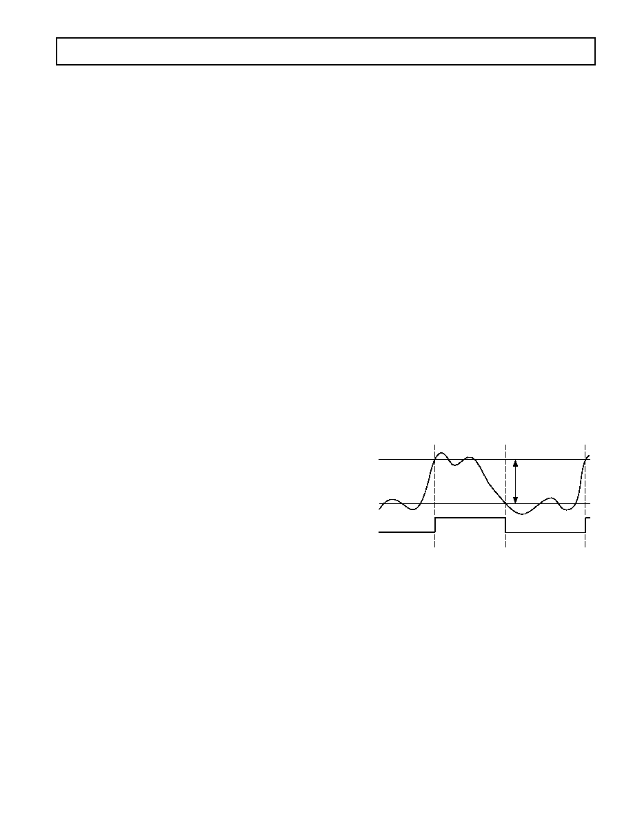
THERM LIMIT
TEMP
100%
HYSTERESIS ( C)
Figure 16.
THERM Limit Operation
REV. 0
18
ADT7463
LIMITS, STATUS REGISTERS, AND INTERRUPTS
Limit Values
Associated with each measurement channel on the ADT7463
are high and low limits. These can form the basis of system
status monitoring: a Status bit can be set for any out-of-limit
condition and detected by polling the device. Alternatively,
SMBALERT interrupts can be generated to flag a processor or
microcontroller of out-of-limit conditions.
8-Bit Limits
The following is a list of 8-bit limits on the ADT7463:
Voltage Limit Registers
Reg. 0x44 2.5 V Low Limit = 0x00 default
Reg. 0x45 2.5 V High Limit = 0xFF default
Reg. 0x46 V
CCP
Low Limit = 0x00 default
Reg. 0x47 V
CCP
High Limit = 0xFF default
Reg. 0x48 V
CC
Low Limit = 0x00 default
Reg. 0x49 V
CC
High Limit = 0xFF default
Reg. 0x4A 5 V Low Limit = 0x00 default
Reg. 0x4B 5 V High Limit = 0xFF default
Reg. 0x4C 12 V Low Limit = 0x00 default
Reg. 0x4D 12 V High Limit = 0xFF default
Temperature Limit Registers
Reg. 0x4E Remote 1 Temp Low Limit = 0x81 default
Reg. 0x4F Remote 1 Temp High Limit = 0x7F default
Reg. 0x6A Remote 1
THERM
THERM
THERM
THERM
THERM Limit = 0x64 default
Reg. 0x50 Local Temp Low Limit = 0x81 default
Reg. 0x51 Local Temp High Limit = 0x7F default
Reg. 0x6B Local
THERM
THERM
THERM
THERM
THERM Limit = 0x64 default
Reg. 0x52 Remote 2 Temp Low Limit = 0x81 default
Reg. 0x53 Remote 2 Temp High Limit = 0x7F default
Reg. 0x6C Remote 2
THERM
THERM
THERM
THERM
THERM Limit = 0x64 default
Therm Limit Register
Reg. 0x7A
THERM
THERM
THERM
THERM
THERM Limit = 0x00 default
16-Bit Limits
The Fan TACH measurements are 16-bit results. The Fan
TACH limits are also 16 bits, consisting of a High Byte and
Low Byte. Since fans running under speed or stalled are nor-
mally the only conditions of interest, only High Limits exist for
Fan TACHs. Since fan TACH period is actually being mea-
sured, exceeding the limit indicates a slow or stalled fan.
Fan Limit Registers
Reg. 0x54 TACH1 Minimum Low Byte = 0xFF default
Reg. 0x55 TACH1 Minimum High Byte = 0xFF default
Reg. 0x56 TACH2 Minimum Low Byte = 0xFF default
Reg. 0x57 TACH2 Minimum High Byte = 0xFF default
Reg. 0x58 TACH3 Minimum Low Byte = 0xFF default
Reg. 0x59 TACH3 Minimum High Byte = 0xFF default
Reg. 0x5A TACH4 Minimum Low Byte = 0xFF default
Reg. 0x5B TACH4 Minimum High Byte = 0xFF default
Out-of-Limit Comparisons
Once all limits have been programmed, the ADT7463 can be
enabled for monitoring. The ADT7463 will measure all param-
eters in round-robin format and set the appropriate Status bit
for out-of-limit conditions. Comparisons are done differently
depending on whether the measured value is being compared to
a high or low limit.
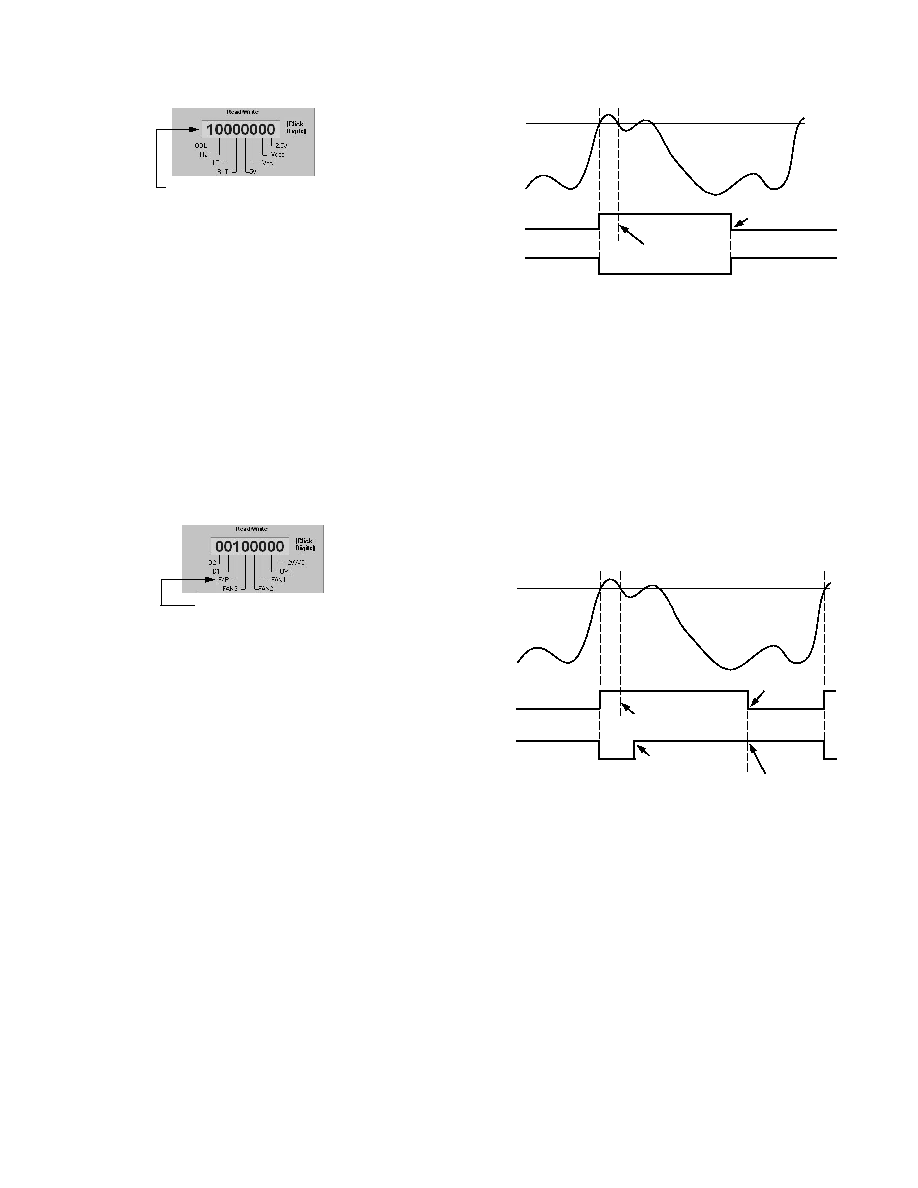
HIGH LIMIT: > COMPARISON PERFORMED
LOW LIMIT: < OR = COMPARISON PERFORMED
NO
INT
LOW LIMIT
TEMP >
LOW LIMIT
Figure 17. Temperature > Low Limit: No
INT
REV. 0
ADT7463
19
INT
LOW LIMIT
TEMP =
LOW LIMIT
Figure 18. Temperature = Low Limit:
INT Occurs
NO
INT
HIGH LIMIT
TEMP =
HIGH LIMIT
21.00C
Figure 19. Temperature = High Limit: No
INT
HIGH LIMIT
INT
TEMP >
HIGH LIMIT
Figure 20. Temperature > High Limit:
INT Occurs
Analog Monitoring Cycle Time
The analog monitoring cycle begins when a 1 is written to the
Start bit (Bit 0) of Configuration Register 1 (Reg. 0x40). The
ADC measures each analog input in turn and as each measure-
ment is completed, the result is automatically stored in the
appropriate value register. This round-robin monitoring cycle
continues unless disabled by writing a 0 to Bit 0 of Configura-
tion Register 1.
As the ADC will normally be left to free-run in this manner, the
time taken to monitor all the analog inputs will normally not be
of interest, as the most recently measured value of any input can
be read out at any time.
For applications where the monitoring cycle time is important,
it can easily be calculated.
The total number of channels measured is:
Four dedicated supply voltage inputs
3.3 V
STBY
or +5 V supply (V
CC
pin)
Local temperature
Two remote temperatures
As mentioned previously, the ADC performs round-robin con-
versions and takes 11.38 ms for each voltage measurement,
12 ms for a local temperature reading, and 25.5 ms for each
remote temperature reading.
The total monitoring cycle time for averaged voltage and tem-
perature monitoring is therefore nominally:
(5 11.38) + 12 + (2 25.5) = 120 ms
Fan TACH measurements are made in parallel and are n ot
synchronized with the analog measurements in any way.
Status Registers
The results of limit comparisons are stored in Status Registers 1
and 2. The Status Register bit for each channel reflects the
status of the last measurement and limit comparison on that
channel. If a measurement is within limits, the corresponding
status register bit will be cleared to 0. If the measurement is out-
of-limits, the corresponding status register bit will be set to 1.
The state of the various measurement channels may be polled
by reading the Status Registers over the serial bus. In Bit 7
(OOL) of Status Register 1 (Reg. 0x41), 1 means that an out-
of-limit event has been flagged in Status Register 2. This means
that you need only read Status Register 2 when this bit is set.
Alternatively, Pin 10 or Pin 22 can be configured as an
SMBALERT output. This will automatically notify the system
supervisor of an out-of-limit condition. Reading the Status
registers clears the appropriate status bit as long as the error
condition that caused the interrupt has cleared. Status Register
bits are "sticky." Whenever a Status bit gets set, indicating an
out-of-limit condition, it will remain set even if the event that
caused it has gone away (until read). The only way to clear the
status bit is to read the Status Register after the event has gone
away. Interrupt Status Mask Registers (Reg. 0x74, 0x75) allow
individual interrupt sources to be masked from causing an
SMBALERT. However, if one of these masked interrupt
sources goes out-of-limit, its associated status bit will get set in
the Interrupt Status Registers.
REV. 0
20
ADT7463
OOL = 1 DENOTES A PARAMETER
MONITORED THROUGH STATUS REG 2
IS OUT-OF-LIMIT
Figure 21. Status Register 1
Status Register 1 (Reg. 0x41)
Bit 7 (OOL) = 1, denotes a bit in Status Register 2 is set and
Status Register 2 should be read.
Bit 6 (R2T) = 1, Remote 2 Temp High or Low Limit has been
exceeded.
Bit 5 (LT) = 1, Local Temp High or Low Limit has been
exceeded.
Bit 4 (R1T) = 1, Remote 1 Temp High or Low Limit has been
exceeded.
Bit 3 (5 V) = 1, 5 V High or Low Limit has been exceeded.
Bit 2 (V
CC
) = 1, V
CC
High or Low Limit has been exceeded.
Bit 1 (V
CCP
) = 1, V
CCP
High or Low Limit has been exceeded.
Bit 0 (2.5 V) = 1, 2.5 V High or Low Limit has been exceeded.
F4P = 1, FAN4 OR
THERM
TIMER IS OUT-OF-LIMIT
Figure 22. Status Register 2
Status Register 2 (Reg. 0x42)
Bit 7 (D2) = 1, indicates an open or short on D2+/D2 inputs.
Bit 6 (D1) = 1, indicates an open or short on D2+/D2 inputs.
Bit 5 (F4P) = 1, indicates Fan 4 has dropped below minimum
speed. Alternatively, indicates that
THERM limit has been
exceeded if the
THERM function is used.
Bit 4 (FAN3) = 1, indicates Fan 3 has dropped below mini-
mum speed.
Bit 3 (FAN2) = 1, indicates Fan 2 has dropped below mini-
mum speed.
Bit 2 (FAN1) = 1, indicates Fan 1 has dropped below mini-
mum speed.
Bit 1 (OVT) = 1, indicates that a
THERM overtemperature
limit has been exceeded.
Bit 0 (12V/VC) = 1, 12 V High or Low Limit has been
exceeded. If the VID Code change function is used, this bit
indicates a change in VID Code on the VID0 to VID5 inputs.
SMBALERT Interrupt Behavior
The ADT7463 can be polled for status, or an
SMBALERT
interrupt can be generated for out-of-limit conditions. It is
important to note how the
SMBALERT output and status bits
behave when writing Interrupt Handler software.
"STICKY"
STATUS
BIT
HIGH LIMIT
TEMPERATURE
SMBALERT
CLEARED ON READ
(TEMP BELOW LIMIT)
TEMP BACK IN LIMIT
(STATUS BIT STAYS SET)
Figure 23.
SMBALERT and Status Bit Behavior
Figure 23 shows how the
SMBALERT output and "sticky"
status bits behave. Once a limit is exceeded, the corresponding
status bit gets set to 1. The status bit remains set until the error
condition subsides and the Status Register gets read. The status
bits are referred to as "sticky" since they remain set until read
by software. This ensures that an out-of-limit event cannot be
missed if software is polling the device periodically. Note that
the
SMBALERT output remains low for the entire duration
that a reading is out-of-limit and until the Status Register has
been read. This has implications on how software handles the
interrupt.
HANDLING SMBALERT INTERRUPTS
To prevent the system from being tied up servicing interrupts, it
is recommend to handle the
SMBALERT interrupt as follows:
" STICKY"
STATUS
BIT
HIGH LIMIT
TEMPERATURE
SMBALERT
CLEARED ON READ
(TEMP BELOW LIMIT)
TEMP BACK IN LIMIT
(STATUS BIT STAYS SET)
INTERRUPT
MASK BIT SET
INTERRUPT MASK BIT
CLEARED
(
SMBALERT REARMED)
Figure 24. How Masking the Interrupt Source
Affects
SMBALERT Output
1. Detect the
SMBALERT assertion.
2. Enter the interrupt handler.
3. Read the Status Registers to identify the interrupt source.
4. Mask the interrupt source by setting the appropriate Mask
bit in the Interrupt Mask Registers (Reg. 0x74, 0x75).
5. Take the appropriate action for a given interrupt source.
6. Exit the Interrupt Handler.
7. Periodically poll the Status Registers. If the interrupt status bit
has cleared, reset the corresponding Interrupt Mask Bit to 0.
This will cause the
SMBALERT output and status bits to
behave as shown in Figure 24.
Masking Interrupt Sources
Interrupt Mask Registers 1 and 2 are located at Addresses
0x74 and 0x75. These allow individual interrupt sources to
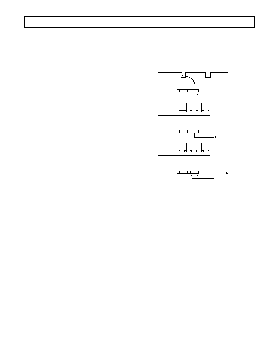
REV. 0
ADT7463
21
be masked out to prevent
SMBALERT interrupts. Note that
masking an interrupt source only prevents the
SMBALERT
output from being asserted; the appropriate Status bit will get
set as normal.
Interrupt Mask Register 1 (Reg. 0x74)
Bit 7 (OOL) = 1, masks
SMBALERT for any alert condition
flagged in Status Register 2.
Bit 6 (R2T) = 1, masks
SMBALERT for Remote 2 Temperature.
Bit 5 (LT) = 1, masks
SMBALERT for Local Temperature.
Bit 4 (R1T) = 1, masks
SMBALERT for Remote 1 Temperature.
Bit 3 (5 V) = 1, masks
SMBALERT for 5 V channel.
Bit 2 (V
CC
) = 1, masks
SMBALERT for V
CC
channel.
Bit 1 (V
CCP
) = 1, masks
SMBALERT for V
CCP
channel.
Bit 0 (2.5 V) = 1, masks
SMBALERT for 2.5 V channel.
Interrupt Mask Register 2 (Reg. 0x75)
Bit 7 (D2) = 1, masks
SMBALERT for Diode 2 errors.
Bit 6 (D1) = 1, masks
SMBALERT for Diode 1 errors.
Bit 5 (FAN4) = 1, masks
SMBALERT for Fan 4 failure. If the
TACH4 pin is being used as the
THERM input, this bit masks
SMBALERT for a THERM event.
Bit 4 (FAN3) = 1, masks
SMBALERT for Fan 3.
Bit 3 (FAN2) = 1, masks
SMBALERT for Fan 2.
Bit 2 (FAN1) = 1, masks
SMBALERT for Fan 1.
Bit 1 (OVT) = 1, masks
SMBALERT for overtemperature
(exceeding
THERM limits).
Bit 0 (12V/VC) = 1, masks
SMBALERT for 12 V channel or
for a VID Code change, depending on the function used.
Enabling the
SMBALERT Interrupt Output
The
SMBALERT interrupt function is disabled by default. Pin
10 or Pin 22 can be reconfigured as an
SMBALERT output to
signal out-of-limit conditions.
CONFIGURING PIN 10 AS
SMBALERT OUTPUT
REGISTER
BIT SETTING
Config Reg 3 (Reg. 0x78)
<0> ALERT = 1
CONFIGURING PIN 22 AS
SMBALERT OUTPUT
REGISTER
BIT SETTING
Config Reg 4 (Reg. 0x7D)
<0> AL2.5V = 1
Therm Input
The ADT7463 has an internal timer to measure
THERM asser-
tion time. For example, the
THERM input may be connected
to the
PROCHOT output of a Pentium 4 CPU and measure
system performance. The
THERM input may also be con-
nected to the output of a trip point temperature sensor.
The timer is started on the assertion of the ADT7463's
THERM input, and stopped on the negation of the pin. The
timer counts
THERM times cumulatively, i.e. the timer
resumes counting on the next
THERM assertion. The THERM
timer will continue to accumulate
THERM assertion times until
the timer is read (it is cleared on read) or until it reaches full
scale. If the counter reaches full scale, it will stop at that reading
until cleared.
The 8-bit
THERM Timer register (Reg. 0x79) is designed such
that Bit 0 will get set to 1 on the first
THERM assertion. Once
the cumulative
THERM assertion time has exceeded 45.52 ms,
Bit 1 of the
THERM timer gets set, and Bit 0 now becomes the
LSB of the timer with a resolution of 22.76 ms.
THERM
TIMER
(REG. 0x79)
THERM
0 0 0 0 0 0 1 0
7 6 5 4 3 2 1 0
THERM ASSERTED
22.76ms
THERM
ACCUMULATE
THERM LOW
ASSERTION TIMES
THERM ASSERTED
45.52ms
0 0 0 0 0 1 0 1
7 6 5 4 3 2 1 0
THERM ASSERTED 113.8ms
(91.04ms + 22.76ms)
THERM
TIMER
(REG. 0x79)
THERM TIMER
(REG. 0x79)
THERM
ACCUMULATE
THERM LOW
ASSERTION TIMES
0 0 0 0 0 0 0 1
7 6 5 4 3 2 1 0
Figure 25. Understanding the
THERM Timer
Figure 25 illustrates how the
THERM timer behaves as the
THERM input is asserted and negated. Bit 0 gets set on the
first
THERM assertion detected. This bit remains set until
such time as the cumulative
THERM assertions exceed
45.52 ms. At this time, Bit 1 of the
THERM timer gets set,
and Bit 0 is cleared. Bit 0 now reflects timer readings with a
resolution of 22.76 ms.
When using the
THERM timer, be aware of the following:
After a
THERM timer read (Reg. 0x79):
a) The contents of the timer get cleared on read.
b) The F4P bit (Bit 5) of Status Register 2 needs to be cleared
(assuming the
THERM limit has been exceeded).
If the
THERM timer is read during a THERM assertion, then
the following will happen:
a) The contents of the timer are cleared.
b) Bit 0 of the
THERM timer is set to 1 (since a THERM
assertion is occurring).
c) The
THERM timer increments from zero.
d) If the
THERM limit (Reg. 0x7A) = 0x00, then the F4P bit
gets set.
Generating
SMBALERT Interrupts from THERM Events
The ADT7463 can generate
SMBALERTs when a program-
mable
THERM limit has been exceeded. This allows the
systems designer to ignore brief, infrequent
THERM assertions,
while capturing longer
THERM events. Register 0x7A is the
THERM Limit Register. This 8-bit register allows a limit from
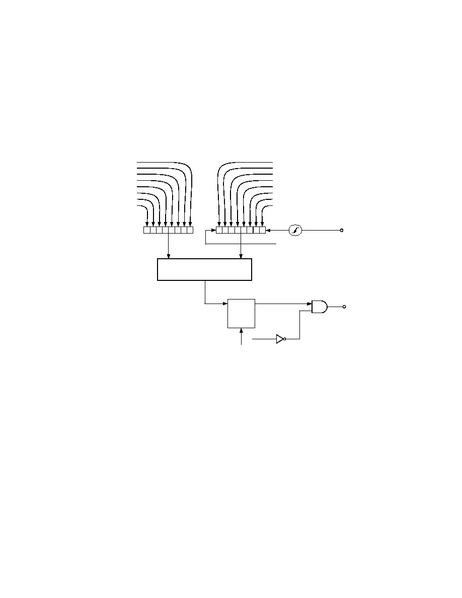
REV. 0
22
ADT7463
7 6 5 4 3 2 1 0
22.76ms
45.52ms
THERM
91.04ms
182.08ms
364.16ms
728.32ms
1.457s
2.914s
IN
OUT
RESET
LATCH
STATUS REGISTER 2
CLEARED
ON READ
F4P BIT (BIT 5)
MASK REGISTER 2
(REG. 0x75)
1 = MASK
SMBALERT
F4P BIT (BIT 5)
THERM TIMER CLEARED ON READ
COMPARATOR
THERM
TIMER
(REG. 0x79)
7
6
5
4
3
2
1
0
22.76ms
45.52ms
91.04ms
182.08ms
364.16ms
728.32ms
1.457s
2.914s
THERM LIMIT
(REG. 0x7A)
Figure 26. Functional Diagram of ADT7463's
THERM Monitoring Circuitry
Configuring the Desired
THERM Behavior
1. Configure the desired pin as the
THERM input.
Setting Bit 1 (PHOT) of Configuration Register 3 (Reg. 0x78)
enables the
THERM monitoring functionality. This is
enabled on Pin 14 by default.
Setting Bit 1 (TH5V) of Configuration Register 4 (Reg.
0x7D) enables
THERM monitoring on Pin 20 (Bit 1 of
Configuration Register 3 must also be set). Pin 14 can be
used as TACH4.
2. Select the desired fan behavior for
THERM events.
Setting Bit 2 (BOOST bit) of Configuration Register 3
(Reg. 0x78) causes all fans to run at 100% duty cycle when-
ever
THERM gets asserted. This allows fail-safe system
cooling. If this bit = 0, the fans will run at their current
settings and will not be affected by
THERM events.
3. Select whether
THERM events should generate
SMBALERT interrupts.
Bit 5 (F4P) of Mask Register 2 (Reg. 0x75), when set,
masks out
SMBALERTs when the THERM limit value
gets exceeded. This bit should be cleared if
SMBALERTs
based on
THERM events are required.
4. Select a suitable
THERM limit value.
This value determines whether an
SMBALERT is generated
on the first
THERM assertion, or only if a cumulative THERM
assertion time limit is exceeded. A value of 0x00 causes an
SMBALERT to be generated on the first THERM assertion.
5. Select a
THERM monitoring time.
This is how often OS or BIOS level software checks the
THERM timer. For example, BIOS could read the THERM
timer once an hour to determine the cumulative
THERM
assertion time. If, for example, the total
THERM assertion
time is <22.76 ms in Hour 1, >182.08 ms in Hour 2, and
>5.825 s in Hour 3, this can indicate that system perfor-
mance is degrading significantly since
THERM is asserting
more frequently on an hourly basis.
0 seconds (first
THERM assertion) to 5.825 seconds to be set
before an
SMBALERT is generated. The THERM Timer value
is compared with the contents of the
THERM Limit Register. If
the
THERM Timer value exceeds the THERM Limit value,
then the F4P bit (Bit 5) of Status Register 2 gets set, and an
SMBALERT is generated. Note that the F4P bit (Bit 5) of
Mask Register 2 (Reg. 0x75) will mask out
SMBALERTs if this
bit is set to 1, although the F4P bit of Interrupt Status Register 2
will still get set if the
THERM Limit is exceeded.
Figure 26 is a Functional Block Diagram of the
THERM timer,
limit, and associated circuitry. Writing a value of 0x00 to the
THERM Limit Register (Reg. 0x7A) causes SMBALERT to
be generated on the first
THERM assertion. A THERM Limit
value of 0x01 generates an
SMBALERT once cumulative THERM
assertions exceed 45.52 ms.
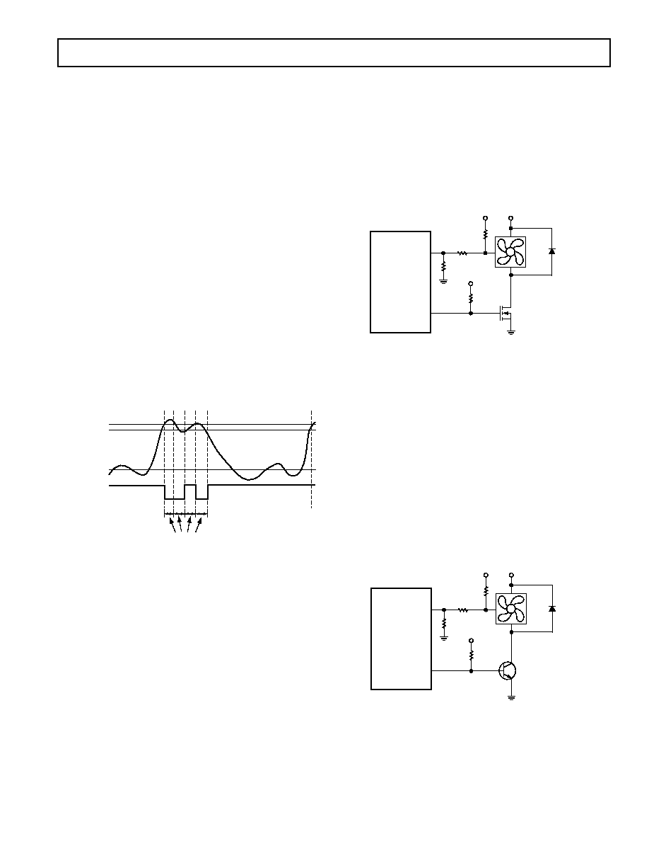
REV. 0
ADT7463
23
Alternatively, OS or BIOS level software can time-stamp
when the system is powered on. If an
SMBALERT is gener-
ated due to the
THERM limit being exceeded, another
time-stamp can be taken. The difference in time can be
calculated for a fixed
THERM limit time. For example, if it
takes one week for a
THERM limit of 2.914 s to be
exceeded and the next time it takes only 1 hour, then this is
an indication of a serious degradation in system performance.
Configuring the ADT7463
THERM Pin as an Output
In addition to the ADT7463 being able to monitor
THERM as
an input, the ADT7463 can optionally drive
THERM low as an
output. The user can preprogram system critical thermal limits.
If the temperature exceeds a thermal limit by 0.25
°C, THERM
will assert low. If the temperature is still above the thermal limit
on the next monitoring cycle,
THERM will stay low. THERM
will remain asserted low until the temperature is equal to or
below the thermal limit. Since the temperature for that channel
is measured only every monitoring cycle, once
THERM asserts
it is guaranteed to remain low for at least one monitoring cycle.
The
THERM pin can be configured to assert low if the
Remote 1, Local, or Remote 2 Temperature
THERM Limits get
exceeded by 0.25
°C. The THERM Limit Registers are at loca-
tions 0x6A, 0x6B, and 0x6C respectively. Setting Bit 3 of
Registers 0x5F, 0x60, and 0x61 enables the
THERM output
feature for the Remote 1, Local, and Remote 2 Temperature
channels, respectively. Figure 27 shows how the
THERM pin
asserts low as an output in the event of a critical overtemperature.
THERM LIMIT
+0.25 C
THERM LIMIT
TEMP
THERM
ADT7463
MONITORING
CYCLE
Figure 27. Asserting
THERM as an Output, Based
on Tripping
THERM Limits
FAN DRIVE USING PWM CONTROL
The ADT7463 uses Pulsewidth Modulation (PWM) to control
fan speed. This relies on varying the duty cycle (or on/off ratio)
of a square wave applied to the fan to vary the fan speed. The
external circuitry required to drive a fan using PWM control is
extremely simple. A single NMOSFET is the only drive device
required. The specifications of the MOSFET depend on the
maximum current required by the fan being driven. Typical
notebook fans draw a nominal 170 mA, and so SOT devices can
be used where board space is a concern. In desktops, fans can
typically draw 250 mA300 mA each. If you drive several fans
in parallel from a single PWM output or drive larger server fans,
the MOSFET will need to handle the higher current requirements.
The only other stipulation is that the MOSFET should have a
gate voltage drive, V
GS
< 3.3 V for direct interfacing to the
PWM_OUT pin. V
GS
can be greater than 3.3 V as long as the
pull-up on the gate is tied to 5 V. The MOSFET should also
have a low on resistance to ensure that there is not significant
voltage drop across the FET. This would reduce the voltage
applied across the fan and therefore the maximum operating
speed of the fan.
Figure 28 shows how a 3-wire fan may be driven using PWM
control.
ADT7463
TACH/AIN
PWM
4.7k
10k
10k
10k
3.3V
12V
12V
12V
FAN
Q1
NDT3055L
TACH
1N4148
Figure 28. Driving a 3-Wire Fan Using an
N-Channel MOSFET
Figure 28 uses a 10 k
pull-up resistor for the TACH signal. This
assumes that the TACH signal is open-collector from the fan. In
all cases, the TACH signal from the fan must be kept below 5 V
maximum to prevent damaging the ADT7463. If in doubt as to
whether the fan used has an open-collector or totem pole
TACH output, use one of the input signal conditioning circuits
shown in the Fan Speed Measurement section of the data sheet.
Figure 29 shows a fan drive circuit using an NPN transistor
such as a general-purpose MMBT2222. While these devices are
inexpensive, they tend to have much lower current handling
capabilities and higher on-resistance than MOSFETs. When
choosing a transistor, care should be taken to ensure that it
meets the fan's current requirements.
Ensure that the base resistor is chosen such that the transistor is
saturated when the fan is powered on.
ADT7463
TACH/AIN
PWM
4.7k
10k
10k
470
3.3V
12V
12V
12V
FAN
Q1
MMBT2222
1N4148
TACH
Figure 29. Driving a 3-Wire Fan Using an NPN Transistor
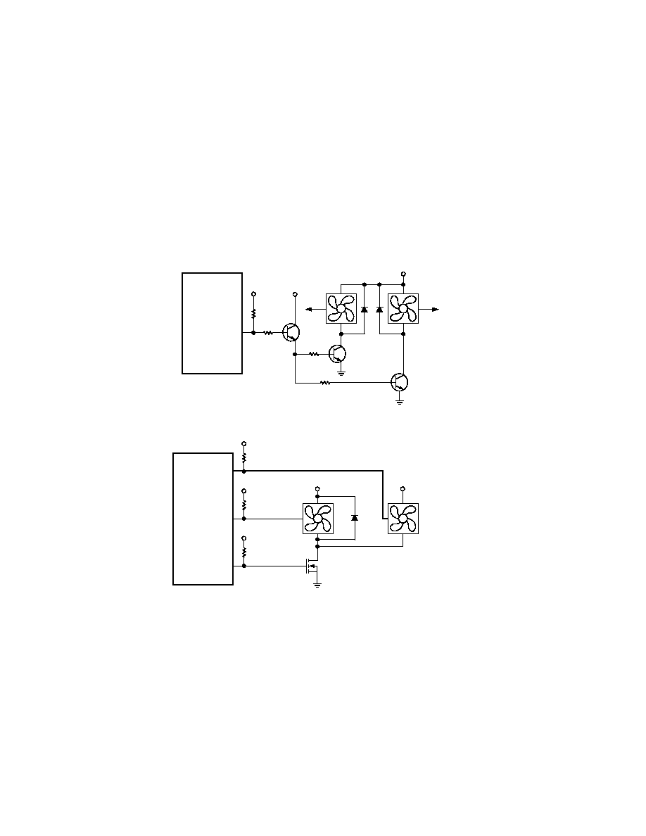
REV. 0
24
ADT7463
ADT7463
PWM3
2.2k
1k
3.3V
Q1
MMBT3904
3.3V
10
TACH3
Q2
MMBT2222
10
TACH4
12V
Q3
MMBT2222
1N4148
Figure 30. Interfacing Two Fans in Parallel to the PWM3 Output Using Low Cost NPN Transistors
ADT7463
TACH4
10k
TYPICAL
3.3V
TACH
TACH3
10k
TYPICAL
3.3V
PWM3
10k
TYPICAL
3.3V
+V
Q1
NDT3055L
5V OR
12V FAN
TACH
5V OR 12V
FAN
+V
1N4148
Figure 31. Interfacing Two Fans in Parallel to the PWM3 Output Using a Single N-Channel MOSFET
Driving Two Fans from PWM3
Note that the ADT7463 has four TACH inputs available for fan
speed measurement, but only three PWM drive outputs. If a
fourth fan is being used in the system, it should be driven from
the PWM3 output in parallel with the third fan. Figure 30 shows
how to drive two fans in parallel using low cost NPN transistors.
Figure 31 is the equivalent circuit using the NDT3055L
MOSFET. Note that since the MOSFET can handle up to
3.5 A, it is simply a matter of connecting another fan directly in
parallel with the first.
Care should be taken in designing drive circuits with transistors
and FETs to ensure that the PWM Pins are not required to
source current, and that they sink less than the 8 mA maximum
current specified on the data sheet.
Driving up to Three Fans From PWM2
TACH measurements for fans are synchronized to particular
PWM channels, e.g., TACH1 is synchronized to PWM1.
TACH3 and TACH4 are both synchronized to PWM3 so
PWM3, can drive 2 fans. Alternatively, PWM2 can be pro-
grammed to synchronize TACH2, TACH3, and TACH4 to the
PWM2 output. This allows PWM2 to drive two or three fans.
In this case, the drive circuitry looks the same as shown in
Figures 30 and 31. The SYNC bit in Register 0x62 enables this
function.
<4> (SYNC) ENHANCE ACOUSTICS REG 1 (0x62)
SYNC = 1 Synchronizes TACH2, TACH3, and TACH4 to
PWM2.
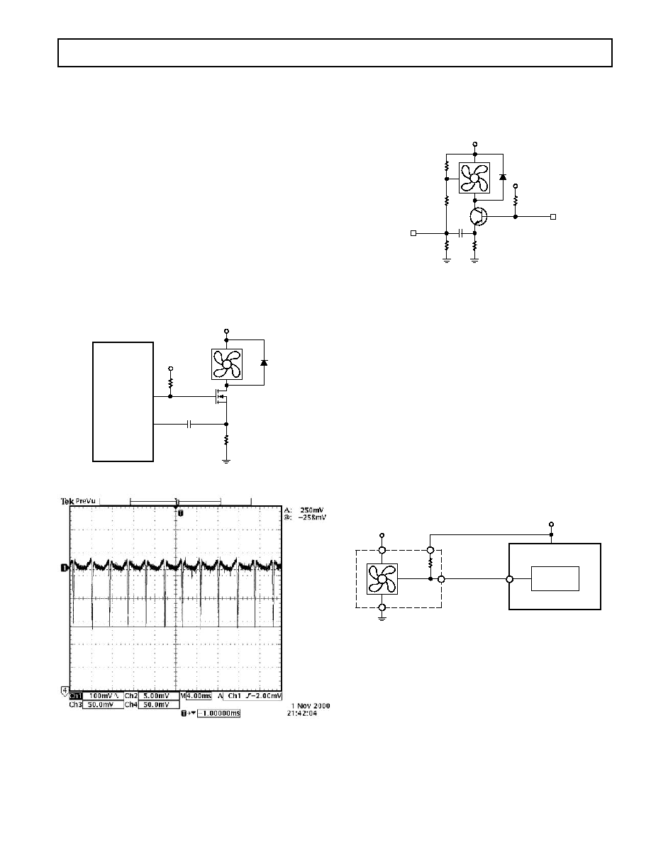
REV. 0
ADT7463
25
Driving 2-Wire Fans
Figure 32 shows how a 2-wire fan may be connected to the
ADT7463. This circuit allows the speed of a 2-wire fan to be
measured, even though the fan has no dedicated TACH signal.
A series resistor, R
SENSE
, in the fan circuit converts the fan
commutation pulses into a voltage. This is ac-coupled into the
ADT7463 through the 0.01
µF capacitor. On-chip signal
conditioning allows accurate monitoring of fan speed. The
value of R
SENSE
chosen depends upon the programmed input
threshold and the current drawn by the fan. For fans drawing
approximately 200 mA, a 2
R
SENSE
value is suitable when the
threshold is programmed as 40 mV. For fans that draw more
current, such as larger desktop or server fans, R
SENSE
may be
reduced for the same programmed threshold. The smaller the
threshold programmed the better, since more voltage will be
developed across the fan and the fan will spin faster. Figure 33
shows a typical plot of the sensing waveform at a TACH/AIN
pin. The most important thing is that the voltage spikes (either
negative going or positive going) are more than 40 mV in ampli-
tude. This allows fan speed to be reliably determined.
ADT7463
TACH/AIN
PWM
10k
TYPICAL
3.3V
+V
Q1
NDT3055L
5V OR
12V FAN
R
SENSE
2
TYPICAL
0.01 F
1N4148
Figure 32. Driving a 2-Wire Fan
Figure 33. Fan Speed Sensing Waveform at
TACH/AIN Pin
LAYING OUT 2-WIRE AND 3-WIRE FANS
Figure 34 shows how to lay out a common circuit arrangement
for 2-wire and 3-wire fans. Some components will not be popu-
lated, depending on whether a 2-wire or 3-wire fan is being used.
3.3V OR 5V
TACH/AIN
PWM
12V OR 5V
Q1
MMBT2222
R4
R5
R3
C1
R2
R1
FOR 3-WIRE FANS:
POPULATE R1, R2, R3
R4 = 0
C1 = UNPOPULATED
FOR 2-WIRE FANS:
POPULATE R4, C1
R1, R2, R3 UNPOPULATED
1N4148
Figure 34. Planning for 2-Wire or 3-Wire Fans on a PCB
TACH Inputs
Pins 11, 12, 9, and 14 are open-drain TACH inputs intended
for fan speed measurement.
Signal conditioning in the ADT7463 accommodates the slow rise
and fall times typical of fan tachometer outputs. The maximum
input signal range is 0 V to 5 V, even where V
CC
is less than 5 V.
In the event that these inputs are supplied from fan outputs that
exceed 0 V to 5 V, either resistive attenuation of the fan signal
or diode clamping must be included to keep inputs within an
acceptable range.
Figures 35a to 35d show circuits for most common fan
TACH outputs.
If the fan TACH output has a resistive pull-up to V
CC
, it can
be connected directly to the fan input, as shown in Figure 35a.
12V
ADT7463
FAN SPEED
COUNTER
TACH
TACH
OUTPUT
PULL-UP
4.7k
TYP
V
CC
Figure 35a. Fan with TACH Pull-Up to +V
CC
If the fan output has a resistive pull-up to 12 V (or other voltage
greater than 5 V) then the fan output can be clamped with a
Zener diode, as shown in Figure 35b. The Zener diode voltage
should be chosen so that it is greater than V
IH
of the TACH
input but less than 5 V, allowing for the voltage tolerance of the
Zener. A value of between 3 V and 5 V is suitable.
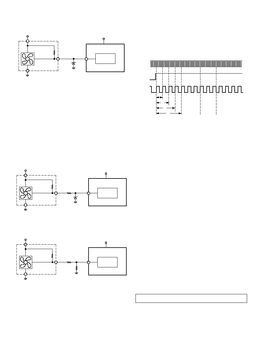
REV. 0
26
ADT7463
ADT7463
FAN SPEED
COUNTER
TACH
TACH
OUTPUT
V
CC
ZD1*
*CHOOSE ZD1 VOLTAGE APPROX 0.8 V
CC
12V
PULL-UP
4.7k
TYP
Figure 35b. Fan with TACH Pull-Up to Voltage
> 5 V, e.g., 12 V) Clamped with Zener Diode
If the fan has a strong pull-up (less than 1 k
) to 12 V or a
totem-pole output, then a series resistor can be added to limit
the Zener current, as shown in Figure 35c. Alternatively, a
resistive attenuator may be used, as shown in Figure 35d.
R1 and R2 should be chosen such that:
2
2
1
2
5
V
V
<
×
+
+
(
)
<
V
R
R
R
R
PULLUP
PULLUP
/
The fan inputs have an input resistance of nominally 160 k
to
ground, so this should be taken into account when calculating
resistor values.
With a pull-up voltage of 12 V and pull-up resistor less than
1 k
, suitable values for R1 and R2 would be 100 k and
47 k
. This will give a high input voltage of 3.83 V.
5V OR 12V
ADT7463
FAN SPEED
COUNTER
TACH
TACH
OUTPUT
PULL-UP TYP
<1k
OR
TOTEM POLE
V
CC
FAN
ZD1
ZENER*
*CHOOSE ZD1 VOLTAGE APPROX 0.8 V
CC
R1
10k
Figure 35c. Fan with Strong TACH Pull-Up to
> V
CC
or Totem-Pole Output, Clamped with Zener
and Resistor
12V
ADT7463
FAN SPEED
COUNTER
TACH
TACH
OUTPUT
<1k
V
CC
R2*
*SEE TEXT
R1*
Figure 35d. Fan with Strong TACH Pull-Up to
> V
CC
or Totem-Pole Output, Attenuated with R1/R2
Fan Speed Measurement
The fan counter does not count the fan TACH output pulses
directly because the fan speed may be less than 1000 RPM and
it would take several seconds to accumulate a reasonably large
and accurate count. Instead, the period of the fan revolution is
measured by gating an on-chip 90 kHz oscillator into the input of
a 16-bit counter for N periods of the fan TACH output (Figure 36),
so the accumulated count is actually proportional to the fan
tachometer period and inversely proportional to the fan speed.
1
2
3
4
CLOCK
PWM
TACH
Figure 36. Fan Speed Measurement
N, the number of pulses counted, is determined by the settings
of Register 0x7B (Fan Pulses Per Revolution Register). This
register contains two bits for each fan, allowing one, two
(default), three, or four TACH pulses to be counted.
Fan Speed Measurement Registers
The Fan Tachometer Readings are 16-bit values consisting of a
2-byte read from the ADT7463.
Reg. 0x28 TACH1 Low Byte = 0x00 default
Reg. 0x29 TACH1 High Byte = 0x00 default
Reg. 0x2A TACH2 Low Byte = 0x00 default
Reg. 0x2B TACH2 High Byte = 0x00 default
Reg. 0x2C TACH3 Low Byte = 0x00 default
Reg. 0x2D TACH3 High Byte = 0x00 default
Reg. 0x2E TACH4 Low Byte = 0x00 default
Reg. 0x2F TACH4 High Byte = 0x00 default
Reading Fan Speed from the ADT7463
If fan speeds are being measured, this involves a 2-register read
for each measurement. The low byte should be read first. This
causes the high byte to be frozen until both High and Low Byte
registers have been read from. This prevents erroneous TACH
readings.
The Fan Tachometer Reading registers report back the number
of 11.11
µs period clocks (90 kHz oscillator) gated to the fan
speed counter, from the rising edge of the first fan TACH pulse
to the rising edge of the third fan TACH pulse (assuming two
pulses per revolution are being counted). Since the device is
essentially measuring the fan TACH period, the higher the
count value the slower the fan is actually running. A 16-bit Fan
Tachometer reading of 0xFFFF indicates either that the fan has
stalled or is running very slowly (< 100 RPM).
HIGH LIMIT: > COMPARISON PERFORMED
Since the actual fan TACH period is being measured, exceeding
a Fan TACH Limit by 1 will set the appropriate Status bit and
can be used to generate an
SMBALERT.

REV. 0
ADT7463
27
Fan TACH Limit Registers
The Fan TACH Limit Registers are 16-bit values consisting of
two bytes.
Reg. 0x54 TACH1 Minimum Low Byte = 0xFF default
Reg. 0x55 TACH1 Minimum High Byte = 0xFF default
Reg. 0x56 TACH2 Minimum Low Byte = 0xFF default
Reg. 0x57 TACH2 Minimum High Byte = 0xFF default
Reg. 0x58 TACH3 Minimum Low Byte = 0xFF default
Reg. 0x59 TACH3 Minimum High Byte = 0xFF default
Reg. 0x5A TACH4 Minimum Low Byte = 0xFF default
Reg. 0x5B TACH4 Minimum High Byte = 0xFF default
Fan Speed Measurement Rate
The Fan TACH readings are normally updated once every
second.
The FAST bit (Bit 3) of Configuration Register 3 (Reg. 0x78),
when set, updates the Fan TACH readings every 250 ms.
If any of the fans are not being driven by a PWM channel but
are powered directly from 5 V or 12 V, its associated dc bit in
Configuration Register 3 should be set. This allows TACH
readings to be taken on a continuous basis for fans connected
directly to a dc source.
Calculating Fan Speed
Assuming a fan with a two pulses/revolution (and two pulses/rev
being measured) fan speed is calculated by:
Fan Speed (RPM) = (90,000 60)/Fan Tach Reading
where,
Fan Tach Reading = 16-bit Fan Tachometer Reading
Example:
TACH1 High Byte (Reg 0x29) = 0x17
TACH1 Low Byte (Reg 0x28) = 0xFF
What is Fan 1 speed in RPM?
Fan 1 TACH reading = 0x17FF = 6143 decimal.
RPM = (f 60)/Fan 1 TACH reading
RPM = (90000 60)/6143
Fan Speed = 879 RPM
Fan Pulses Per Revolution
Different fan models can output either 1, 2, 3, or 4 TACH
pulses per revolution. Once the number of fan TACH pulses
has been determined, it can be programmed into the Fan
Pulses Per Revolution Register (Reg. 0x7B) for each fan.
Alternatively, this register can be used to determine the num-
ber or pulses/revolution output by a given fan. By plotting fan
speed measurements at 100% speed with different pulses/rev
setting, the smoothest graph with the lowest ripple determines
the correct pulses/rev value.
Fan Pulses Per Revolution Register
<1:0> FAN1 default = 2 pulses per rev.
<3:2> FAN2 default = 2 pulses per rev.
<5:4> FAN3 default = 2 pulses per rev.
<7:6> FAN4 default = 2 pulses per rev.
00 = 1 pulse per rev.
01 = 2 pulses per rev.
10 = 3 pulses per rev.
11 = 4 pulses per rev.
2-Wire Fan Speed Measurements
The ADT7463 is capable of measuring the speed of 2-wire fans,
i.e., fans without TACH outputs. To do this, the fan must be
interfaced as shown in the Fan Drive Circuitry section of the
data sheet. In this case, the TACH inputs need to be repro-
grammed as analog inputs, AIN.
CONFIGURATION REGISTER 2 (REG. 0x73)
Bit 3 (AIN4) = 1, Pin 14 is reconfigured to measure the speed
of a 2-wire fan using an external sensing resistor and coupling
capacitor.
Bit 2 (AIN3) = 1, Pin 9 is reconfigured to measure the speed
of a 2-wire fan using an external sensing resistor and coupling
capacitor.
Bit 1 (AIN2) = 1, Pin 12 is reconfigured to measure the speed
of a 2-wire fan using an external sensing resistor and coupling
capacitor.
Bit 0 (AIN1) = 1, Pin 11 is reconfigured to measure the speed
of a 2-wire fan using an external sensing resistor and coupling
capacitor.
AIN Switching Threshold
Having configured the TACH inputs as AIN inputs for 2-wire
measurements, you can select the sensing threshold for the
AIN signal.
CONFIGURATION REGISTER 4 (REG. 0x7D)
<3:2> AINL These two bits define the input threshold for
2-wire fan speed measurements.
00 = 20 mV
01 = 40 mV
10 = 80 mV
11 = 130 mV
Fan Spin-Up
The ADT7463 has a unique fan spin-up function. It will spin
the fan at 100% PWM duty cycle until two TACH pulses are
detected on the TACH input. Once two pulses have been
detected, the PWM duty cycle will go to the expected running
value, e.g., 33%. The advantage of this is that fans have dif-
ferent spin-up characteristics and will take different times to
overcome inertia. The ADT7463 just runs the fans fast enough
to overcome inertia and will be quieter on spin-up than fans
programmed to spin-up for a given spin-up time.
Fan Start-Up Timeout
To prevent false interrupts being generated as a fan spins up
(since it is below running speed), the ADT7463 includes a Fan
Start-Up Timeout function. This is the time limit allowed for
two TACH pulses to be detected on spin-up. For example, if 2
seconds Fan Start-Up Timeout is chosen and no TACH pulses
occur within 2 seconds of the start of spin-up, a fan fault is
detected and flagged in the Interrupt Status Registers.

REV. 0
28
ADT7463
PWM1 CONFIGURATION (REG. 0x5C)
<2:0> SPIN
These bits control the Start-Up timeout for
PWM1.
000 = No startup timeout
001 = 100 ms
010 = 250 ms (default)
011 = 400 ms
100 = 667 ms
101 = 1 s
110 = 2 s
111 = 4 s
PWM2 CONFIGURATION (REG. 0x5D)
<2:0> SPIN
These bits control the Start-Up timeout for
PWM2.
000 = No startup timeout
001 = 100 ms
010 = 250 ms (default)
011 = 400 ms
100 = 667 ms
101 = 1 s
110 = 2 s
111 = 4 s
PWM3 CONFIGURATION (REG. 0x5E)
<2:0> SPIN
These bits control the Start-Up timeout for
PWM3.
000 = No startup timeout
001 = 100 ms
010 = 250 ms (default)
011 = 400 ms
100 = 667 ms
101 = 1 s
110 = 2 s
111 = 4 s
Disabling Fan Start-Up Timeout
Although Fan Start-Up makes fan spin-ups much quieter than
fixed-time spin-ups, the option exists to use fixed spin-up
times. Bit 5 (FSPDIS) = 1 in Configuration Register 1 (Reg.
0x40) disables the spin-up for two TACH pulses. Instead, the
fan will spin up for the fixed time as selected in Registers
0x5C0x5E.
PWM Logic State
The PWM outputs can be programmed high for 100% duty
cycle (noninverted) or low for 100% duty cycle (inverted).
PWM1 Configuration (Reg. 0x5C)
<4> INV
0 = logic high for 100% PWM duty cycle
1 = logic low for 100% PWM duty cycle
PWM2 Configuration (Reg. 0x5D)
<4> INV
0 = logic high for 100% PWM duty cycle
1 = logic low for 100% PWM duty cycle
PWM3 Configuration (Reg. 0x5E)
<4> INV
0 = logic high for 100% PWM duty cycle
1 = logic low for 100% PWM duty cycle
PWM Drive Frequency
The PWM drive frequency can be adjusted for the application.
Registers 0x5F0x61 configure the PWM frequency for
PWM1PWM3, respectively.
PWM1 FREQUENCY REGISTERS (REG. 0x5F0x61)
<2:0> FREQ 000 = 11.0 Hz
001 = 14.7 Hz
010 = 22.1 Hz
011 = 29.4 Hz
100 = 35.3 Hz (default)
101 = 44.1 Hz
110 = 58.8 Hz
111 = 88.2 Hz
Fan Speed Control
The ADT7463 can control fan speed using two different modes.
The first is Automatic Fan Speed Control Mode. In this mode
fan speed is automatically varied with temperature and without
CPU intervention, once initial parameters are set up. The
advantage of this is in the case of the system hanging, the user is
guaranteed that the system is protected from overheating. The
Automatic Fan Speed Control incorporates a feature called
Dynamic T_min calibration. This feature reduces the design
effort required to program the Automatic Fan Speed Control
Loop. For more information and how to program the Automatic
Fan Speed Control Loop and Dynamic T_min calibration, see
the Automatic Fan Speed Control Loop application note.
The second fan speed control method is Manual Fan Speed
Control which is described in the next paragraph.
Manual Fan Speed Control
The ADT7463 allows the Duty Cycle of any PWM output to be
manually adjusted. This can be useful if you wish to change fan
speed in software or want to adjust PWM duty cycle output for
test purposes. Bits <7:5> of Registers 0x5C0x5E (PWM Con-
figuration) control the behavior of each PWM output.
PWM CONFIGURATION (REG. 0x5C0x5E)
<7:5> BHVR 111 = Manual Mode
Once under Manual Control, each PWM output may be manu-
ally updated by writing to registers 0x300x32 (PWMx Current
Duty Cycle Registers).
Programming the PWM
Current Duty Cycle Registers
The PWM
Current Duty Cycle Registers are 8-bit registers that
allow the PWM duty cycle for each output to be set anywhere
from 0% to 100% in steps of 0.39%.
The value to be programmed into the PWM
MIN
register is
given by:
Value decimal
PWM
MIN
(
)
=
0 39
.
Example 1: For a PWM duty cycle of 50%,
Value (decimal) = 50/0.39 = 128 decimal
Value = 128 decimal or 0x80.
Example 2: For a PWM duty cycle of 33%,
Value (decimal) = 33/0.39 = 85 decimal
Value = 85 decimal or 0x54.
PWM DUTY CYCLE REGISTERS
Reg. 0x30 PWM1 Duty Cycle = 0xFF (100% default)
Reg. 0x31 PWM2 Duty Cycle = 0xFF (100% default)
Reg. 0x32 PWM3 Duty Cycle = 0xFF (100% default)

REV. 0
ADT7463
29
By reading the PWMx Current Duty Cycle Registers, you can
keep track of the current duty cycle on each PWM output, even
when the fans are running in Automatic Fan Speed Control
Mode or Acoustic Enhancement Mode.
VARY PWM DUTY
CYCLE WITH 8-BIT
RESOLUTION
Figure 37. Control PWM Duty Cycle Manually
with a Resolution of 0.39%
OPERATING FROM 3.3 V STANDBY
The ADT7463 has been specifically designed to operate from a
3.3 V STBY supply. In computers that support S3 and S5
states, the core voltage of the processor will be lowered in these
states. If using the Dynamic T
MIN
Mode, lowering the core
voltage of the processor would change the CPU temperature
and change the dynamics of the system under dynamic T
MIN
control. Likewise, when monitoring
THERM, the THERM
timer should be disabled during these states.
DYNAMIC T
MIN
CONTROL REGISTER 1 (REG. 0x36)
<1> V
CCP
LO = 1 When the power is supplied from 3.3 V STBY
and V
CCP
voltage drops below the V
CCP
Low Limit, the follow-
ing occurs:
· Status Bit 1 (V
CCP
) in Status Register 1 gets set.
·
SMBALERT gets generated if enabled.
·
THERM monitoring is disabled. The THERM timer
should hold its value prior to the S3 or S5 state.
· Dynamic T
MIN
control is disabled. This prevents T
MIN
from
being adjusted due to an S3 or S5 state.
· The ADT7463 is prevented from entering the shutdown state.
Once the core voltage, V
CCP
, goes above the V
CCP
Low Limit, every-
thing gets re-enabled and the system resumes normal operation.
Note that since other voltages can drop or be turned off during
a low power state, these voltage channels will set status bits or
generate
SMBALERTs. It is still necessary to mask out these
channels prior to entering a low power state using the Interrupt
Mask Registers. When exiting the low power state, the mask bits
can be cleared. This prevents the device from generating
unwanted
SMBALERTs during the low power state.
XOR TREE TEST MODE
The ADT7463 includes an XOR Tree Test Mode. This mode is
useful for in-circuit test equipment at board-level testing. By
applying stimulus to the pins included in the XOR Tree, it is
possible to detect opens or shorts on the system board. Figure 38
shows the signals that are exercised in the XOR Tree Test Mode.
PWM1/XTO
PWM3
PWM2
TACH4
TACH3
TACH2
TACH1
VID4
VID3
VID2
VID1
VID0
Figure 38. XOR Tree Test
The XOR Tree Test is invoked by setting Bit 0 (XEN) of the
XOR Tree Test Enable Register (Reg. 0x6F).

REV. 0
30
ADT7463
Table IV. ADT7463 Registers
Address
R/W
Description
Bit 7
Bit 6
Bit 5
Bit 4
Bit 3
Bit 2
Bit 1
Bit 0
Default
Lockable?
0x20
R
2.5 V Reading
9
8
7
6
5 4
3
2
0x00
0x21
R
V
CCP
Reading
9
8
7
6
5 4
3
2
0x00
0x22
R
V
CC
Reading
9
8
7
6
5 4
3
2
0x00
0x23
R
5 V Reading
9
8
7
6
5 4
3
2
0x00
0x24
R
12 V Reading
9
8
7
6
5 4
3
2
0x00
0x25
R
Remote 1 Temperature
9
8
7
6
5 4
3
2
0x80
0x26
R
Local Temperature
9
8
7
6
5 4
3
2
0x80
0x27
R
Remote 2 Temperature
9
8
7
6
5 4
3
2
0x80
0x28
R
TACH1 Low Byte
7
6
5
4
3
2
1
0
0x00
0x29
R
TACH1 High Byte
15
14
13
12
11
10
9
8
0x00
0x2A
R
TACH2 Low Byte
7
6
5
4
3
2
1
0
0x00
0x2B
R
TACH2 High Byte
15
14
13
12
11
10
9
8
0x00
0x2C
R
TACH3 Low Byte
7
6
5
4
3
2
1
0
0x00
0x2D
R
TACH3 High Byte
15
14
13
12
11
10
9
8
0x00
0x2E
R
TACH4 Low Byte
7
6
5
4
3
2
1
0
0x00
0x2F
R
TACH4 High Byte
15
14
13
12
11
10
9
8
0x00
0x30
R/W
PWM1 Current Duty Cycle
7
6
5
4
3
2
1
0
0xFF
0x31
R/W
PWM2 Current Duty Cycle
7
6
5
4
3
2
1
0
0xFF
0x32
R/W
PWM3 Current Duty Cycle
7
6
5
4
3
2
1
0
0xFF
0x33
R/W
Remote 1 Operating Point
7
6
5
4
3
2
1
0
0x64
YES
0x34
R/W
Local Temp Operating Point
7
6
5
4
3
2
1
0
0x64
YES
0x35
R/W
Remote 2 Operating Point
7
6
5
4
3
2
1
0
0x64
YES
0x36
R/W
Dynamic T
MIN
Control Reg 1
R2T LT R1T PHTR2 PHTL PHTR1 V
CC
PLO CYR2
0x00
YES
0x37
R/W
Dynamic T
MIN
Control Reg 2
CYR2 CYR2 CYL CYL CYL CYR1 CYR1 CYR1
0x00
YES
0x3D
R
Device ID Register
7
6
5
4
3
2
1
0
0x27
0x3E
R
Company ID Number
7
6
5
4
3
2
1
0
0x41
0x3F
R
Revision Number
VER
VER
VER
VER
STP
STP
STP
STP
0x62
0x40
R/W
Configuration Register 1
V
CC
TODIS
FSPDIS
V I
FSPD
RDY
LOCK
STRT
0x00
YES
0x41
R
Interrupt Status Register 1
OOL
R2T
LT
R1T
5V
V
CC
V
CCP
2.5V
0x00
0x42
R
Interrupt Status Register 2
D2
D1
5
FAN3
FAN2
FAN1
OVT
12V/VC
0x00
0x43
R/W
VID Register
VIDSEL THLD
5
VID4
VID3
VID2
VID1
VID0
0xFF
0x44
R/W
2.5 V Low Limit
7
6
5
4
3
2
1
0
0x00
0x45
R/W
2.5 V High Limit
7
6
5
4
3
2
1
0
0xFF
0x46
R/W
V
CCP
Low Limit
7
6
5
4
3
2
1
0
0x00
0x47
R/W
V
CCP
High Limit
7
6
5
4
3
2
1
0
0xFF
0x48
R/W
V
CC
Low Limit
7
6
5
4
3
2
1
0
0x00
0x49
R/W
V
CC
High Limit
7
6
5
4
3
2
1
0
0xFF
0x4A
R/W
5 V Low Limit
7
6
5
4
3
2
1
0
0x00
0x4B
R/W
5 V High Limit
7
6
5
4
3
2
1
0
0xFF
0x4C
R/W
12 V Low Limit
7
6
5
4
3
2
1
0
0x00
0x4D
R/W
12 V High Limit
7
6
5
4
3
2
1
0
0xFF
0x4E
R/W
Remote 1 Temp Low Limit
7
6
5
4
3
2
1
0
0x81
0x4F
R/W
Remote 1 Temp High Limit
7
6
5
4
3
2
1
0
0x7F
0x50
R/W
Local Temp Low Limit
7
6
5
4
3
2
1
0
0x81
0x51
R/W
Local Temp High Limit
7
6
5
4
3
2
1
0
0x7F
0x52
R/W
Remote 2 Temp Low Limit
7
6
5
4
3
2
1
0
0x81
0x53
R/W
Remote 2 Temp High Limit
7
6
5
4
3
2
1
0
0x7F
0x54
R/W
TACH1 Minimum Low Byte
7
6
5
4
3
2
1
0
0xFF
0x55
R/W
TACH1 Minimum High Byte
15
14
13
12
11
10
9
8
0xFF
0x56
R/W
TACH2 Minimum Low Byte
7
6
5
4
3
2
1
0
0xFF
0x57
R/W
TACH2 Minimum High Byte
15
14
13
12
11
10
9
8
0xFF
0x58
R/W
TACH3 Minimum Low Byte
7
6
5
4
3
2
1
0
0xFF
0x59
R/W
TACH3 Minimum High Byte
15
14
13
12
11
10
9
8
0xFF
0x5A
R/W
TACH4 Minimum Low Byte
7
6
5
4
3
2
1
0
0xFF
0x5B
R/W
TACH4 Minimum High Byte
15
14
13
12
11
10
9
8
0xFF

REV. 0
ADT7463
31
Table IV. ADT7463 Registers (continued)
Address
R/W Description
Bit 7
Bit 6
Bit 5
Bit 4
Bit 3
Bit 2
Bit 1
Bit 0
Default
Lockable?
0x5C
R/W PWM1 Configuration Register
BHVR
BHVR
BHVR
INV
SLOW
SPIN
SPIN
SPIN
0x62
YES
0x5D
R/W PWM2 Configuration Register
BHVR
BHVR
BHVR
INV
SLOW
SPIN
SPIN
SPIN
0x62
YES
0x5E
R/W PWM3 Configuration Register
BHVR
BHVR
BHVR
INV
SLOW
SPIN
SPIN
SPIN
0x62
YES
0x5F
R/W Remote 1 T
RANGE
/PWM 1 Freq
RANGE RANGE RANGE
RANGE THRM FREQ
FREQ
FREQ
0xC4
YES
0x60
R/W Local T
RANGE
/PWM 2 Freq
RANGE RANGE RANGE
RANGE THRM FREQ
FREQ
FREQ
0xC4
YES
0x61
R/W Remote 2 T
RANGE
/PWM 3 Freq
RANGE RANGE RANGE
RANGE THRM FREQ
FREQ
FREQ
0xC4
YES
0x62
R/W Enhance Acoustics Reg 1
MIN3
MIN2
MIN1
SYNC
EN1
ACOU
ACOU
ACOU
0x00
YES
0x63
R/W Enhance Acoustics Reg 2
EN2
ACOU2 ACOU2
ACOU2 EN3
ACOU3 ACOU3 ACOU3 0x00
YES
0x64
R/W PWM1 Min Duty Cycle
7
6
5
4
3
2
1
0
0x80
YES
0x65
R/W PWM2 Min Duty Cycle
7
6
5
4
3
2
1
0
0x80
YES
0x66
R/W PWM3 Min Duty Cycle
7
6
5
4
3
2
1
0
0x80
YES
0x67
R/W Remote 1 Temp T
MIN
7
6
5
4
3
2
1
0
0x5A
YES
0x68
R/W Local Temp T
MIN
7
6
5
4
3
2
1
0
0x5A
YES
0x69
R/W Remote 2 Temp T
MIN
7
6
5
4
3
2
1
0
0x5A
YES
0x6A
R/W Remote 1
THERM Limit
7
6
5
4
3
2
1
0
0x64
YES
0x6B
R/W Local
THERM Limit
7
6
5
4
3
2
1
0
0x64
YES
0x6C
R/W Remote 2
THERM Limit
7
6
5
4
3
2
1
0
0x64
YES
0x6D
R/W Remote 1 Local Hysteresis
HYSR1
HYSR1
HYSR1
HYSR1 HYSL
HYSL
HYSL
HYSL
0x44
YES
0x6E
R/W Remote 2 Temp Hysteresis
HYSR2
HYSR2
HYSR2
HYSR2 RES
RES
RES
RES
0x40
YES
0x6F
R/W XOR Tree Test Enable
RES
RES
RES
RES
RES
RES
RES
XEN
0x00
YES
0x70
R/W Remote 1 Temperature Offset
7
6
5
4
3
2
1
0
0x00
YES
0x71
R/W Local Temperature Offset
7
6
5
4
3
2
1
0
0x00
YES
0x72
R/W Remote 2 Temperature Offset
7
6
5
4
3
2
1
0
0x00
YES
0x73
R/W Configuration Register 2
SHDN
CONV
ATTN
AVG
AIN4
AIN3
AIN2
AIN1
0x00
YES
0x74
R/W Interrupt Mask 1 Register
OOL
R2T
LT
R1T
5V
V
CC
V
CCP
2.5V
0x00
0x75
R/W Interrupt Mask 2 Register
D2
D1
5
FAN3
FAN2
FAN1
OVT
12V/VC 0x00
0x76
R/W Extended Resolution 1
5V
5V
V
CC
V
CC
V
CCP
V
CCP
2.5V
2.5V
0x00
0x77
R/W Extended Resolution 2
TDM2
TDM2
LTMP
LTMP
TDM1
TDM1
12V
12V
0x00
0x78
R/W Configuration Register 3
DC4
DC3
DC2
DC1
FAST
BOOST PHOT
ALERT 0x00
YES
0x7B
R/W Fan Pulses per Revolution
FAN4
FAN4
FAN3
FAN3
FAN2
FAN2
FAN1
FAN1
0x55
0x7D
R/W Configuration Register 4
RES
RES
RES
RES
AINL
AINL
TH5V
AL2.5V 0x00
YES
0x7E
R
Test Register 1
DO NOT WRITE TO THESE REGISTERS
0x00
YES
0x7F
R
Test Register 2
DO NOT WRITE TO THESE REGISTERS
0x00
YES

REV. 0
32
ADT7463
Table V. Voltage Reading Registers (Power on Default = 0x00)
Register Address
R/W
Description
0x20
Read Only
2.5 V Reading (8 MSBs of reading)
0x21
Read Only
V
CCP
Reading: holds processor core voltage measurement (8 MSBs of reading)
0x22
Read Only
V
CC
Reading: measures V
CC
through the V
CC
pin (8 MSBs of reading)
0x23
Read Only
5 V Reading (8 MSBs of reading)
0x24
Read Only
12 V Reading (8 MSBs of reading)
If the extended resolution bits of these readings are also being read, the Extended Resolution registers (Reg. 0x76, 0x77) should be read first. Once the Extended
Resolution registers get read, the associated MSB reading registers get frozen until read. Both the
Extended Resolution Registers and the MSB registers get frozen.
Table VI. Temperature Reading Registers (Power on Default = 0x80)
Register Address
R/W
Description
0x25
Read Only
Remote 1 Temperature Reading
* (8 MSBs of reading)
0x26
Read Only
Local Temperature Reading (8 MSBs of reading)
0x27
Read Only
Remote 2 Temperature Reading
* (8 MSBs of reading)
These temperature readings are in twos complement format.
*Note that a reading of 0x80 in a temperature reading register indicates a diode fault (open or short) on that channel. If the extended resolution bits of these readings
are also being read, the Extended Resolution registers (Reg. 0x76, 0x77) should be read first. Once the Extended Resolution registers get read, all associated MSB
reading registers get frozen until read. Both the Extended Resolution Registers and the MSB registers get frozen.
Table VII. Fan Tachometer Reading Registers (Power on Default = 0x00)
Register Address
R/W
Description
0x28
Read Only
TACH1 Low Byte
0x29
Read Only
TACH1 High Byte
0x2A
Read Only
TACH2 Low Byte
0x2B
Read Only
TACH2 High Byte
0x2C
Read Only
TACH3 Low Byte
0x2D
Read Only
TACH3 High Byte
0x2E
Read Only
TACH4 Low Byte
0x2F
Read Only
TACH4 High Byte
These registers count the number of 11.11
µs periods (based on an internal 90 kHz clock) that occur between a number of consec tive fan TACH pulses (default = 2).
The number of TACH pulses used to count can be changed using the Fan Pulses Per Revolution Register (Reg. 0x7B). This allows the fan speed to be accurately mea-
sured. Since a valid Fan Tachometer reading requires that two bytes are read, the low byte MUST be read first. Both the low and high bytes are then frozen until read.
At power-on, these registers contain 0x0000 until such time as the first valid fan TACH measurement is read in to these registers. This prevents false interrupts from
occurring while the fans are spinning up.
A count of 0xFFFF indicates that a fan is:
1. Stalled or Blocked (object jamming the fan)
2. Failed (internal circuitry destroyed)
3. Not Populated (the ADT7463 expects to see a fan connected to
each TACH. If a fan is not connected to that TACH, its TACH
minimum high and low byte should be set to 0xFFFF.)
4. Alternate Function, e.g., TACH4 reconfigured as
THERM pin
5. 2-Wire Instead of 3-Wire Fan

REV. 0
ADT7463
33
Table VIII. Current PWM Duty Cycle Registers (Power-On Default = 0xFF)
Register Address
R/W
Description
0x30
Read/Write
PWM1 Current Duty Cycle (0% to 100% duty cycle = 0x00 to 0xFF)
0x31
Read/Write
PWM2 Current Duty Cycle (0% to 100% duty cycle = 0x00 to 0xFF)
0x32
Read/Write
PWM3 Current Duty Cycle (0% to 100% duty cycle = 0x00 to 0xFF)
These registers reflect the PWM duty cycle driving each fan at any given time. When in Automatic Fan Speed Control Mode, the ADT7463 reports the PWM duty
cycles back through these registers. The PWM duty cycle values will vary according to temperature in Automatic Fan Speed Control Mode. During fan startup, these
registers report back 0x00. In Software Mode, the PWM duty cycle outputs can be set to any duty cycle value by writing to these registers.
Table IX. Operating Point Registers (Power-on Default = 0x64)
Register Address
R/W
*
Description
0x33
Read/Write
Remote 1 Operating Point Register (default = 100 C)
0x34
Read/Write
Local Temp Operating Point Register (default = 100 C)
0x35
Read/Write
Remote 2 Operating Point Register (default = 100 C)
These registers set the target Operating Point for each temperature channel when the Dynamic T
MIN
Control feature is enabled.
The fans being controlled will be adjusted to maintain temperature about an Operating Point.
*These registers become read-only when the Configuration Register 1 Lock bit is set to 1. Any subsequent attempts to write to these registers will fail.

REV. 0
34
ADT7463
Table X. Register 0x36 Dynamic T
MIN
Control Register 1 (Power-On Default = 0x00)
Bit
Name R/W
Description
<0>
CYR2
Read/Write
MSB of 3-Bit Remote 2 Cycle Value. The other two bits of the code reside in Dynamic T
MIN
Control Register 2 (Reg. 0x37). These three bits define the delay time between making sub-
sequent T
MIN
adjustments in the control loop, in terms of number of monitoring cycles.
The system will have associated thermal time constants that need to be found to optimize
the response of fans and the control loop.
<1>
V
CCP
LO
Read/Write
V
CCP
LO = 1. When the power is supplied from 3.3VSTANDBY and the core voltage
(V
CCP
) drops below its V
CCP
low limit value (Reg. 0x46), the following occurs:
Status bit 1 in Status Register 1 gets set.
SMBALERT gets generated if enabled.
PROCHOT monitoring is disabled.
Dynamic T
MIN
control is disabled.
The device is prevented from entering shutdown.
Everything re-enabled once V
CCP
increases above V
CCP
low limit.
<2>
PHTR1
Read/Write
PHTR1 = 1 copies the Remote 1 current temperature to the Remote 1 Operating Point
Register if
THERM gets asserted. The operating point will contain the temperature at
which
THERM is asserted. This allows the system to run as quietly as possible without
system performance being affected. PHTR1 = 0 ignores any
THERM assertions on the
THERM pin. The Remote 1 Operating Point Register will reflect its programmed value.
<3>
PHTL
Read/Write
PHTL = 1 copies the local channel's current temperature to the Local Operating Point
Register if
THERM gets asserted. The operating point will contain the temperature at
which
THERM is asserted. This allows the system to run as quietly as possible without
system performance being affected. PHTL = 0 ignores any
THERM assertions on the
THERM pin. The Local Temp Operating Point Register will reflect its programmed value.
<4>
PHTR2
Read/Write
PHTR2 = 1 copies the Remote 2 current temperature to the Remote 2 Operating Point
Register if
THERM gets asserted. The operating point will contain the temperature at
which
THERM is asserted. This allows the system to run as quietly as possible without
system performance being affected. PHTR2 = 0 ignores any
THERM assertions on the
THERM pin. The Remote 2 Operating Point Register will reflect its programmed value.
<5>
R1T
Read/Write
R1T = 1 enables dynamic T
MIN
control on the Remote 1 Temperature channel. The
chosen T
MIN
value will be dynamically adjusted based on the current temperature, oper-
ating point, and high and low limits for this zone. R1T = 0 disables dynamic T
MIN
con-
trol. The T
MIN
value chosen will not be adjusted and the channel will behave as described
in the Automatic Fan Control section.
<6>
LT
Read/Write
LT = 1 enables dynamic T
MIN
control on the Local Temperature channel. The chosen
T
MIN
value will be dynamically adjusted based on the current temperature, operating
point, and high and low limits for this zone. LT = 0 disables dynamic T
MIN
control. The
T
MIN
value chosen will not be adjusted and the channel will behave as described in the
Automatic Fan Control section.
<7>
R2T
Read/Write
R2T = 1 enables dynamic T
MIN
control on the Remote 2 Temperature channel. The
chosen T
MIN
value will be dynamically adjusted based on the current temperature,
operating point, and high and low limits for this zone. R2T = 0 disables dynamic T
MIN
control. The T
MIN
value chosen will not be adjusted and the channel will behave as
described in the Automatic Fan Control section.
*This register becomes read-only when the Configuration Register 1 Lock bit is set to 1. Any subsequent attempts to write to this register will fail.

REV. 0
ADT7463
35
Table XI. Register 0x37 Dynamic T
MIN
Control Register 2 (Power-On Default = 0x00)
Bit
Name R/W
*
Description
<2:0>
CYR1
Read/Write
3-bit Remote 1 Cycle Value. These three bits define the delay time between making subse-
quent T
MIN
adjustments in the control loop for Remote 1 channel, in terms of number of
monitoring cycles. The system will have associated thermal time constants that need to be
found to optimize the response of fans and the control loop.
BITS
DECREASE CYCLE
INCREASE CYCLE
000
4 cycles (0.5 s)
8 cycles (1 s)
001
8 cycles (1 s)
16 cycles (2 s)
010
16 cycles (2 s)
32 cycles (4 s)
011
32 cycles (4 s)
64 cycles (8 s)
100
64 cycles (8 s)
128 cycles (16 s)
101
128 cycles (16 s)
256 cycles (32 s)
110
256 cycles (32 s)
512 cycles (64 s)
111
512 cycles (64 s)
1024 cycles (128 s)
<5:3>
CYL
Read/Write
3-bit Local Temp Cycle Value. These three bits define the delay time between making subse-
quent T
MIN
adjustments in the control loop for Local Temp channel, in terms of number
of monitoring cycles. The system will have associated thermal time constants that need to
be found to optimize the response of fans and the control loop.
BITS
DECREASE CYCLE
INCREASE CYCLE
000
4 cycles (0.5 s)
8 cycles (1 s)
001
8 cycles (1 s)
16 cycles (2 s)
010
16 cycles (2 s)
32 cycles (4 s)
011
32 cycles (4 s)
64 cycles (8 s)
100
64 cycles (8 s)
128 cycles (16 s)
101
128 cycles (16 s)
256 cycles (32 s)
110
256 cycles (32 s)
512 cycles (64 s)
111
512 cycles (64 s)
1024 cycles (128 s)
<7:6>
CYR2
Read/Write
2 LSBs of 3-bit Remote 2 Cycle Value. The MSB of the 3-bit code resides in Dynamic
T
MIN
Control Register 1 (Reg. 0x36). These three bits define the delay time between making
subsequent T
MIN
adjustments in the control loop for Remote 2 channel, in terms of num-
ber of monitoring cycles. The system will have associated thermal time constants that
need to be found to optimize the response of fans and the control loop.
BITS
DECREASE CYCLE
INCREASE CYCLE
000
4 cycles (0.5 s)
8 cycles (1 s)
001
8 cycles (1 s)
16 cycles (2 s)
010
16 cycles (2 s)
32 cycles (4 s)
011
32 cycles (4 s)
64 cycles (8 s)
100
64 cycles (8 s)
128 cycles (16 s)
101
128 cycles (16 s)
256 cycles (32 s)
110
256 cycles (32 s)
512 cycles (64 s)
111
512 cycles (64 s)
1024 cycles (128 s)
*This register becomes read-only when the Configuration Register 1 Lock bit is set to 1. Any subsequent attempts to write to this register will fail.

REV. 0
36
ADT7463
Table XII. Register 0x40 Configuration Register 1 (Power-On Default = 0x00)
Bit
Name
R/W
Description
<0>
STRT
Read/Write
Logic 1 enables monitoring and PWM control outputs based on the limit settings pro-
grammed. Logic 0 disables monitoring and PWM control based on the default power-up
limit settings. Note that the limit values programmed are preserved even if a logic 0 is
written to this bit and the default settings are enabled. This bit becomes read-only and
cannot be changed once Bit 1 (LOCK bit) has been written. All limit registers should be
programmed by BIOS before setting this bit to 1. (Lockable.)
<1>
LOCK
Write Once
Logic 1 locks all limit values to their current settings. Once this bit is set, all lockable
registers become read-only and cannot be modified until the ADT7463 is powered down
and powered up again. This prevents rogue programs such as viruses from modifying
critical system limit settings. (Lockable.)
<2>
RDY
Read Only
This bit gets set to 1 by the ADT7463 to indicate that the device is fully powered-up
and ready to begin systems monitoring.
<3>
FSPD
Read/Write
When set to 1, this runs all fans at full speed. Power-on default = 0. This bit does not get
locked at any time.
<4>
V I
Read/Write
BIOS should set this bit to a 1 when the ADT7463 is configured to measure current
from an ADI ADOPT
TM
VRM controller and measure the CPU's core voltage. This will
allow monitoring software to display CPU watts usage. (Lockable.)
<5>
FSPDIS
Read/Write
Logic 1 disables fan spin-up for two TACH pulses. Instead, the PWM outputs will go
high for the entire fan spin-up timeout selected.
<6>
TODIS
Read/Write
When this bit is set to 1, the SMBus timeout feature is disabled. This allows the
ADT7463 to be used with SMBus controllers that cannot handle SMBus
timeouts. (Lockable.)
<7>
V
CC
Read/Write
When this bit is set to 1, the ADT7463 rescales its V
CC
pin to measure a 5 V supply. If
this bit is 0, the ADT7463 measures V
CC
as a 3.3 V supply. (Lockable.)
Table XIII. Register 0x41 Interrupt Status Register 1 (Power-On Default = 0x00)
Bit
Name
R/W
Description
<0>
2.5 V
Read Only
A one indicates the 2.5 V
High or Low limit has been exceeded. This bit gets cleared on
a read of the Status Register only if the error condition has subsided.
<1>
V
CCP
Read Only
A one indicates the V
CCP
High or Low limit has been exceeded. This bit gets cleared on
a read of the Status Register only if the error condition has subsided.
<2>
V
CC
Read Only
A one indicates the V
CC
High or Low limit has been exceeded. This bit gets cleared on a
read of the Status Register only if the error condition has subsided.
<3>
5 V
Read Only
A one indicates the 5 V High or Low limit has been exceeded. This bit gets cleared on a
read of the Status Register only if the error condition has subsided.
<4>
R1T
Read Only
A one indicates the Remote 1 Low or High Temp limit has been exceeded. This bit gets
cleared on a read of the Status Register only if the error condition has subsided.
<5>
LT
Read Only
A one indicates the Local Low or High Temp limit has been exceeded. This bit gets
cleared on a read of the Status Register only if the error condition has subsided.
<6>
R2T
Read Only
A one indicates the Remote 2 Low or High Temp limit has been exceeded. This bit gets
cleared on a read of the Status Register only if the error condition has subsided.
<7>
OOL
Read Only
A one indicates that an Out-of-Limit event has been latched in Status Register 2. This
bit is a logical OR of all status bits in Status Register 2. Software can test this bit in
isolation to determine whether any of the voltage, temperature, or fan speed readings
represented by Status Register 2 are out-of-limit. This saves the need to read Status
Register 2 every interrupt or polling cycle.
ADOPT is a trademark of Analog Devices, Inc.

REV. 0
ADT7463
37
Table XIV. Register 0x42 Interrupt Status Register 2 (Power-On Default = 0x00)
Bit
Name
R/W
Description
<0>
12 V
Read Only
A one indicates the 12 V high or low limit has been exceeded. This bit gets cleared on a
read of the Status Register only if the error condition has subsided. If Pin 21 is config-
ured as VID5, this bit is the VID Change bit. This bit gets set when the levels on VID05
are different than they were 11
µs previously. This can be used to generate an
SMBALERT whenever the VID code changes.
<1>
OVT
Read Only
A one indicates that one of the
THERM overtemperature limits has been
exceeded. This bit gets cleared on a read of the Status Register when the
temperature drops below
THERM T
HYST
.
<2>
FAN1
Read Only
A one indicates that Fan 1 has dropped below minimum speed or has stalled.
This bit does NOT get set when the PWM 1 output is off.
<3>
FAN2
Read Only
A one indicates that Fan 2 has dropped below minimum speed or has stalled.
This bit does NOT get set when the PWM 2 output is off.
<4>
FAN3
Read Only
A one indicates that Fan 3 has dropped below minimum speed or has stalled.
This bit does NOT get set when the PWM 3 output is off.
<5>
F4P
Read Only
A one indicates that Fan 4 has dropped below minimum speed or has stalled.
This bit does NOT get set when the PWM 3 output is off.
Read Only
If Pin 14 or Pin 20 is configured as the
THERM timer input for THERM
monitoring, then this bit gets set when the
THERM assertion time exceeds the
limit programmed in the
THERM Limit Register (Reg. 0x7A).
<6>
D1
Read Only
A one indicates either an open or short circuit on the Thermal Diode 1 inputs.
<7>
D2
Read Only
A one indicates either an open or short circuit on the Thermal Diode 2 inputs.
Table XV. Register 43H VID Register (Power-On Default = 0x00)
Bit
Name
R/W
Description
<4:0>
VID[4:0]
Read Only
The VID[4:0] inputs from the CPU to indicate the expected processor core voltage. On
power-up, these bits reflect the state of the VID Pins even if monitoring is not enabled.
<5>
VID5
Read Only
Reads VID5 from the CPU when Bit 7 = 1. If Bit 7 = 0, then the VID5 bit always
reads back 0 (power-on default).
<6>
THLD
Read/Write
This selects the input switching threshold for the VID inputs. THLD = 0 selects a
threshold of 1 V (V
OL
< 0.8 V, V
IH
> 1.7 V). THLD = 1 lowers the switching threshold
to 0.6 V (V
OL
< 0.4 V, V
IH
> 0.8 V).
<7>
VIDSEL
Read/Write
VIDSEL = 0 configures Pin 21 as the 12 V measurement input (default).
VIDSEL = 1 configures Pin 21 as the VID5 input. This also allows VID code
changes to be detected.
Table XVI. Voltage Limit Registers
Register Address
R/W
Description
Power-On Default
0x44
Read/Write
2.5 V Low Limit
0x00
0x45
Read/Write
2.5 V High Limit
0xFF
0x46
Read/Write
V
CCP
Low Limit
0x00
0x47
Read/Write
V
CCP
High Limit
0xFF
0x48
Read/Write
V
CC
Low Limit
0x00
0x49
Read/Write
V
CC
High Limit
0xFF
0x4A
Read/Write
5 V Low Limit
0x00
0x4B
Read/Write
5 V High Limit
0xFF
0x4C
Read/Write
12 V Low Limit
0x00
0x4D
Read/Write
12 V High Limit
0xFF
Setting the Configuration Register 1 Lock bit has no effect on these registers.
High Limits: An interrupt is generated when a value exceeds its high limit (> comparison).
Low Limits: An interrupt is generated when a value is equal to or below its low limit (
comparison).

REV. 0
38
ADT7463
Table XVII. Temperature Limit Registers
Register Address
R/W
Description
Power-On Default
0x4E
Read/Write
Remote 1 Temp Low Limit
0x81
0x4F
Read/Write
Remote 1 Temp High Limit
0x7F
0x50
Read/Write
Local Temp Low Limit
0x81
0x51
Read/Write
Local Temp High Limit
0x7F
0x52
Read/Write
Remote 2 Temp Low Limit
0x81
0x53
Read/Write
Remote 2 Temp High Limit
0x7F
Exceeding any of these temperature limits by 18C will cause the appropriate status bit to be set in the Interrupt Status Register. Setting the Configuration Register 1
Lock bit has no effect on these registers.
High Limits: An interrupt is generated when a value exceeds its high limit (> comparison).
Low Limits: An interrupt is generated when a value is equal to or below its low limit (
comparison).
Table XVIII. Fan Tachometer Limit Registers
Register Address
R/W
Description
Power-On Default
0x54
Read/Write
TACH1 Minimum Low Byte
0xFF
0x55
Read/Write
TACH1 Minimum High Byte
0xFF
0x56
Read/Write
TACH2 Minimum Low Byte
0xFF
0x57
Read/Write
TACH2 Minimum High Byte
0xFF
0x58
Read/Write
TACH3 Minimum Low Byte
0xFF
0x59
Read/Write
TACH3 Minimum High Byte
0xFF
0x5A
Read/Write
TACH4 Minimum Low Byte
0xFF
0x5B
Read/Write
TACH4 Minimum High Byte
0xFF
Exceeding any of the TACH limit registers by 1 indicates that the fan is running too slowly or has stalled. The appropriate status bit will be set in Interrupt Status
Register 2 to indicate the fan failure. Setting the Configuration Register 1 Lock bit has no effect on these registers.

REV. 0
ADT7463
39
Table XIX. PWM Configuration Registers
Register Address
R/W
*
Description
Power-On Default
0x5C
Read/Write
PWM1 Configuration
0x62
0x5D
Read/Write
PWM2 Configuration
0x62
0x5E
Read/Write
PWM3 Configuration
0x62
Bit
Name
R/W
Description
<2:0>
SPIN
Read/Write
These bits control the startup timeout for PWMx. The PWM output stays high until two
valid TACH rising edges are seen from the fan. If there is not a valid TACH signal during the
fan TACH measurement directly after the Fan Startup Timeout period, then the TACH
measurement will read 0xFFFF and Status Register 2 reflects the Fan Fault. If the TACH
Minimum High and Low Byte contains 0xFFFF or 0x0000, then the Status Register 2
bit will not get set, even if the fan has not started.
000 = No startup timeout
001 = 100 ms
010 = 250 ms (default)
011 = 400 ms
100 = 667 ms
101 = 1 s
110 = 2 s
111 = 4 s
<3>
SLOW
Read/Write
SLOW = 1 makes the Ramp Rates for Acoustic Enhancement four times longer
<4>
INV
Read/Write
This bit inverts the PWM output. The default is 0, which corresponds to a logic high
output for 100% duty cycle. Setting this bit to 1 inverts the PWM output, so 100% duty
cycle corresponds to a logic low output.
<7:5>
BHVR
Read/Write
These bits assign each fan to a particular temperature sensor for localized cooling.
000 = Remote 1 Temp controls PWMx (Automatic Fan Control Mode)
001 = Local Temp controls PWMx (Automatic Fan Control Mode)
010 = Remote 2 Temp controls PWMx (Automatic Fan Control Mode)
011 = PWMx runs full speed (default)
100 = PWMx disabled
111 = Manual Mode. PWM Duty cycle Registers (Reg 0x300x32) become writable.
*These registers become read-only when the Configuration Register 1 Lock bit is set to 1. Any subsequent attempts to write to these registers will fail.

REV. 0
40
ADT7463
Table XX. TEMP T
RANGE
/PWM Frequency Registers
Register Address
R/W
*
Description
Power-On Default
0x5F
Read/Write
Remote 1 T
RANGE
/PWM 1 Frequency
0xC4
0x60
Read/Write
Local Temp T
RANGE
/PWM 2 Frequency
0xC4
0x61
Read/Write
Remote 2 T
RANGE
/PWM 3 Frequency
0xC4
Bit
Name
Read/Write
Description
<2:0>
FREQ
Read/Write
These bits control the PWMx frequency.
000 = 11.0 Hz
001 = 14.7 Hz
010 = 22.1 Hz
011 = 29.4 Hz
100 = 35.3 Hz (default)
101 = 44.1 Hz
110 = 58.8 Hz
111 = 88.2 Hz
<3>
THRM
Read/Write
THRM = 1 causes the
THERM pin (Pin 14 or 20) to assert low as an output when this
temperature channel's
THERM limit has been exceeded by 0.25 C. The THERM pin
will remain asserted until the temperature is equal to or below the
THERM limit. The
minimum time that
THERM asserts for is one monitoring cycle. This allows clock modu-
lation of devices that incorporate this feature.
THRM = 0 makes the
THERM pin act as an input only, e.g., for Pentium 4 PROCHOT
monitoring, when Pin 14 or 20 is configured as
THERM.
<7:4>
RANGE
Read/Write
These bits determine the PWM Duty Cycle versus Temperature Slope for
Automatic Fan Control.
0000 = 2 C
0001 = 2.5 C
0010 = 3.33 C
0011 = 4 C
0100 = 5 C
0101 = 6.67 C
0110 = 8 C
0111 = 10 C
1000 = 13.33 C
1001 = 16 C
1010 = 20 C
1011 = 26.67 C
1100 = 32 C (default)
1101 = 40 C
1110 = 53.33 C
1111 = 80 C
*These registers become read-only when the Configuration Register 1 Lock bit is set. Any further attempts to write to these registers shall have no effect.

REV. 0
ADT7463
41
Table XXI. Register 0x62 Enhance Acoustics Reg 1 (Power-On Default = 0x00)
Bit
Name
R/W
*
Description
<2:0>
ACOU
Read/Write
These bits select the Ramp Rate applied to the PWM1 output. Instead of PWM1 jump-
ing instantaneously to its newly calculated speed, PWM1 will ramp gracefully at the rate
determined by these bits. This feature enhances the acoustics of the fan being driven by
the PWM1 output.
Time Slot Increase
Time for 33% to 100%
000 = 1
35 s
001 = 2
17.6 s
010 = 3
1.8 s
011 = 5
7 s
100 = 8
4.4 s
101 = 12
3 s
110 = 24
1.6 s
111 = 48
0.8 s
<3>
EN1
Read/Write
When this bit is 1, Acoustic Enhancement is enabled on PWM1 output.
<4>
SYNC
Read/Write
SYNC = 1 synchronizes fan speed measurements on TACH2, TACH3, and
TACH4 to PWM3. This allows up to three fans to be driven from PWM3 output and
their speeds to be measured.
SYNC = 0, only TACH3 and TACH4 are synchronized to PWM3 output.
<5>
MIN1
Read/Write
When the ADT7463 is in Automatic Fan Control Mode, this bit defines whether PWM 1
is off (0% duty cycle) or at PWM 1 Minimum Duty Cycle when the controlling tem-
perature is below its T
MIN
Hysteresis value.
0 = 0% duty cycle below T
MIN
Hysteresis
1 = PWM 1 Minimum Duty Cycle below T
MIN
Hysteresis
<6>
MIN2
Read/Write
When the ADT7463 is in Automatic Fan Speed Control Mode, this bit defines whether
PWM 2 is off (0% duty cycle) or at PWM 2 Minimum Duty Cycle when the controlling
temperature is below its T
MIN
Hysteresis value.
0 = 0% duty cycle below T
MIN
Hysteresis
1 = PWM 2 Minimum Duty Cycle below T
MIN
Hysteresis
<7>
MIN3
Read/Write
When the ADT7463 is in Automatic Fan Speed Control Mode, this bit defines whether
PWM 3 is off (0% duty cycle) or at PWM 3 Minimum Duty Cycle when the controlling
temperature is below its T
MIN
Hysteresis value.
0 = 0% duty cycle below T
MIN
Hysteresis
1 = PWM 3 Minimum Duty Cycle below T
MIN
Hysteresis
*This register becomes read-only when the Configuration Register 1 Lock bit is set to 1. Any further attempts to write to this register will have no effect.

REV. 0
42
ADT7463
Table XXII. Register 0x63 Enhance Acoustics Reg 2 (Power-On Default = 0x00)
Bit
Name
R/W
*
Description
<2:0>
ACOU3
Read/Write
These bits select the Ramp Rate applied to the PWM3 output. Instead of PWM3 jump-
ing instantaneously to its newly calculated speed, PWM3 will ramp gracefully at the rate
determined by these bits. This effect enhances the acoustics of the fan being driven by the
PWM3 output.
Time Slot Increase
Time for 33% to 100%
000 = 1
35 s
001 = 2
17.6 s
010 = 3
11.8 s
011 = 5
7 s
100 = 8
4.4 s
101 = 12
3 s
110 = 24
1.6 s
111 = 48
0.8 s
<3>
EN3
Read/Write
When this bit is 1, Acoustic Enhancement is enabled on PWM3 output.
<6:4>
ACOU2
Read/Write
These bits select the Ramp Rate applied to the PWM2 output. Instead of PWM2
jumping instantaneously to its newly calculated speed, PWM2 will ramp gracefully at the
rate determined by these bits. This effect enhances the acoustics of the fans being driven
by the PWM2 output.
Time Slot Increase
Time for 33% to 100%
000 = 1
35 s
001 = 2
17.6 s
010 = 3
11.8 s
011 = 5
7 s
100 = 8
4.4 s
101 = 12
3 s
110 = 24
1.6 s
111 = 48
0.8 s
<7>
EN2
Read/Write
When this bit is 1, Acoustic Enhancement is enabled on PWM2 output.
*This register becomes read-only when the Configuration Register 1 Lock bit is set to 1. Any further attempts to write to this register will have no effect.

REV. 0
ADT7463
43
Table XXIII. PWM Min Duty Cycle Registers
Register Address
R/W
*
Description
Power-On Default
0x64
Read/Write
PWM1 Min Duty Cycle
0x80 (50% duty cycle)
0x65
Read/Write
PWM2 Min Duty Cycle
0x80 (50% duty cycle)
0x66
Read/Write
PWM3 Min Duty Cycle
0x80 (50% duty cycle)
Bit
Name
Read/Write
Description
<7:0>
PWM Duty
Read/Write
These bits define the PWM
MIN
duty cycle for PWMx.
Cycle
0x00 = 0% duty cycle (Fan off)
0x40 = 25% duty cycle
0x80 = 50% duty cycle
0xFF = 100% duty cycle (Fan full speed)
*These registers become read-only when the ADT7463 is in Automatic Fan Control Mode.
Table XXIV. T
MIN
Registers
Register Address
R/W
*
Description
Power-On Default
0x67
Read/Write
Remote 1 Temp T
MIN
0x5A (90 C)
0x68
Read/Write
Local Temp T
MIN
0x5A (90 C)
0x69
Read/Write
Remote 2 Temp T
MIN
0x5A (90 C)
These are the T
MIN
registers for each temperature channel. When the temperature measured exceeds T
MIN
, the appropriate fan will run at minimum speed and
increase with temperature according to T
RANGE
.
*These registers become read-only when the Configuration Register 1 Lock bit is set. Any further attempts to write to these registers shall have no effect.
Table XXV.
THERM Limit Registers
Register Address
R/W
*
Description
Power-On Default
0x6A
Read/Write
Remote 1
THERM Limit
0x64 (100 C)
0x6B
Read/Write
Local
THERM Limit
0x64 (100 C)
0x6C
Read/Write
Remote 2
THERM Limit
0x64 (100 C)
If any temperature measured exceeds its
THERM limit, all PWM outputs will drive their fans at 100% duty cycle. This is a fail-safe mechanism incorporated to cool
the system in the event of a critical overtemperature. It also ensures some level of cooling in the event that software or hardware locks up. If set to 0x80, this feature is
disabled. The PWM output will remain at 100% until the temperature drops below
THERM limit Hysteresis. If the THERM pin is programmed as an output, then
exceeding these limits by 0.25 C can cause the
THERM pin to assert low as an output.
*These registers become read-only when the Configuration Register 1 Lock bit is set to 1. Any further attempts to write to these registers will have no effect.
Table XXVI. Temperature Hysteresis Registers
Register Address
R/W
*
Description
Power-On Default
0x6D
Read/Write
Remote 1, Local Temp Hysteresis
0x44
0x6E
Read/Write
Remote 2 Temp Hysteresis
0x40
Each 4-bit value controls the amount of temperature hysteresis applied to a particular temperature channel. Once the temperature for that channel falls below its T
MIN
value, the fan will remain running at PWM
MIN
duty cycle until the temperature = T
MIN
Hysteresis. Up to 158C of hysteresis may be assigned to any temperature
channel. The hysteresis value chosen will also apply to that temperature channel if its
THERM limit is exceeded. The PWM output being controlled will go to 100% if
the
THERM limit is exceeded and will remain at 100% until the temperature drops below THERM Hysteresis. For acoustic reasons, it is recommended that the
hysteresis value not be programmed less than 48C. Setting the hysteresis value lower than 48C will cause the fan to switch on and off regularly when the temperature is
close to T
MIN
.
*These registers become read-only when the Configuration Register 1 Lock bit is set to 1. Any further attempts to write to these registers will have no effect.

REV. 0
44
ADT7463
Table XXVII. XOR Tree Test Enable
Register Address
R/W
*
Description
Power-On Default
0x6F
Read/Write
XOR Tree Test Enable Register
0x00
<0>
XEN
If the XEN bit is set to 1, the device enters the XOR Tree Test Mode. Clearing the bit
removes the device from the XOR Test Mode.
<7:1>
Reserved
Unused. Do not write to these bits.
*This register becomes read-only when the Configuration Register 1 Lock bit is set to 1. Any further attempts to write to this register will have no effect.
Table XXVIII. Remote 1 Temperature Offset
Register Address
R/W
*
Description
Power-On Default
0x70
Read/Write
Remote 1 Temperature Offset
0x00
<7:0>
Read/Write
Allows a twos complement offset value to be automatically added to or subtracted from
the Remote 1 Temperature reading. This is to compensate for any inherent system offsets
such as PCB trace resistance. LSB value = 0.25
o
C.
*This register becomes read-only when the Configuration Register 1 Lock bit is set to 1. Any further attempts to write to this register will have no effect.
Table XXIX. Local Temperature Offset
Register Address
R/W
*
Description
Power-On Default
0x71
Read/Write
Local Temperature Offset
0x00
<7:0>
Read/Write
Allows a twos complement offset value to be automatically added to or subtracted from
the local temperature reading. LSB value = 0.25
o
C.
*This register becomes read-only when the Configuration Register 1 Lock bit is set to 1. Any further attempts to write to this register will have no effect.
Table XXX. Remote 2 Temperature Offset
Register Address
R/W
*
Description
Power-On Default
0x72
Read/Write
Remote 2 Temperature Offset
0x00
<7:0>
Read/Write
Allows a twos complement offset value to be automatically added to or subtracted from
the Remote 2 Temperature reading. This is to compensate for any inherent system off-
sets such as PCB trace resistance. LSB value = 0.25
o
C.
*This register becomes read-only when the Configuration Register 1 Lock bit is set to 1. Any further attempts to write to this register will have no effect.

REV. 0
ADT7463
45
Table XXXI. Register 0x73 Configuration Register 2 (Power-On Default = 0x00)
Bit
Name
R/W
*
Description
0
AIN1
Read/Write
AIN1 = 0, Speed of 3-wire fans measured using the TACH output from the fan.
AIN1 = 1, Pin 11 is reconfigured to measure the speed of 2-wire fans using an external
sensing resistor and coupling capacitor. AIN voltage threshold is set via Configuration
Register 4 (Reg. 0x7D).
1
AIN2
Read/Write
AIN2 = 0, Speed of 3-wire fans measured using the TACH output from the fan.
AIN2 = 1, Pin 12 is reconfigured to measure the speed of 2-wire fans using an external
sensing resistor and coupling capacitor. AIN voltage threshold is set via Configuration
Register 4 (Reg. 0x7D).
2
AIN3
Read/Write
AIN3 = 0, Speed of 3-wire fans measured using the TACH output from the fan.
AIN3 = 1, Pin 9 is reconfigured to measure the speed of 2-wire fans using an external
sensing resistor and coupling capacitor. AIN voltage threshold is set via Configuration
Register 4 (Reg. 0x7D).
3
AIN4
Read/Write
AIN4 = 0, Speed of 3-wire fans measured using the TACH output from the fan.
AIN4 = 1, Pin 14 is reconfigured to measure the speed of 2-wire fans using an external
sensing resistor and coupling capacitor. AIN voltage threshold is set via Configuration
Register 4 (Reg. 0x7D).
4
AVG
Read/Write
AVG = 1, Averaging on the temperature and voltage measurements is turned off. This
allows measurements on each channel to be made much faster.
5
ATTN
Read/Write
ATTN = 1, the ADT7463 removes the attenuators from the 2.5 V, V
CCP
, 5 V, and
12 V inputs. The inputs can be used for other functions such as connecting up external
sensors.
6
CONV
Read/Write
CONV = 1, the ADT7463 is put into a single-channel ADC Conversion Mode. In this
mode, the ADT7463 can be made to read continuously from one input only, e.g.,
Remote 1 Temperature. It is also possible to start ADC conversions using an external
clock on Pin 11 by setting Bit 2 of Test Register 2 (Reg. 0x7F). This mode could be
useful if, for example, you wanted to characterize/profile CPU temperature quickly. The
appropriate ADC channel is selected by writing to Bits <7:5> of TACH1 Min High
Byte Register (0x55).
Bits <7:5> Reg 0x55
Channel Selected
000
2.5 V
001
V
CCP
010
V
CC
(3.3 V)
011
5 V
100
12 V
101
Remote 1 Temp
110
Local Temp
111
Remote 2 Temp
7
SHDN
Read/Write
SHDN = 1, ADT7463 goes into Shutdown Mode. All PWM outputs assert low (or high
depending on state of INV bit) to switch off all fans. The PWM Current Duty Cycle
registers read 0x00 to indicate that the fans are not being driven.
*This register becomes read-only when the Configuration Register 1 Lock bit is set to 1. Any further attempts to write to this register will have no effect.

REV. 0
46
ADT7463
Table XXXII. Register 0x74 Interrupt Mask Register 1 (Power On Default <7:0> = 0x00)
Bit
Name
R/W
Description
0
2.5 V
Read/Write
A one masks
SMBALERT for out-of-limit conditions on the 2.5 V channel.
1
V
CCP
Read/Write
A one masks
SMBALERT for out-of-limit conditions on the V
CCP
channel.
2
V
CC
Read/Write
A one masks
SMBALERT for out-of-limit conditions on the V
CC
channel.
3
5 V
Read/Write
A one masks
SMBALERT for out-of-limit conditions on the 5 V channel.
4
R1T
Read/Write
A one masks
SMBALERT for out-of-limit conditions on the Remote 1
Temperature channel.
5
LT
Read/Write
A one masks
SMBALERT for out-of-limit conditions on the Local
Temperature channel.
6
R2T
Read/Write
A one masks
SMBALERT for out-of-limit conditions on the Remote 2
Temperature channel.
7
OOL
Read/Write
A one masks
SMBALERT for any out-of-limit condition in Status Register 2.
Table XXXIII. Register 0x75 Interrupt Mask Register 2 (Power On Default <7:0> = 0x00)
Bit
Name
R/W
Description
0
12 V/VC
Read/Write
A one masks
SMBALERT for out-of-limit conditions on the 12 V channel.
1
OVT
Read Only
A one masks
SMBALERT for overtemperature THERM conditions.
2
FAN1
Read/Write
A one masks
SMBALERT for a Fan 1 Fault.
3
FAN2
Read/Write
A one masks
SMBALERT for a Fan 2 Fault.
4
FAN3
Read/Write
A one masks
SMBALERT for a Fan 3 Fault.
5
F4P
Read/Write
A one masks
SMBALERT for a Fan 4 Fault. If the TACH4 pin is being used as the
THERM input, this bit masks SMBALERT for a THERM timer event.
6
D1
Read/Write
A one masks
SMBALERT for a diode open or short on Remote 1 channel.
7
D2
Read/Write
A one masks
SMBALERT for a diode open or short on Remote 2 channel.
Table XXXIV. Register 0x76 Extended Resolution Register 1
Bit
Name
R/W
Description
<1:0>
2.5 V
Read Only
2.5 V LSBs. Holds the 2 LSBs of the 10-bit 2.5 V measurement.
<3:2>
V
CCP
Read Only
V
CCP
LSBs. Holds the 2 LSBs of the 10-bit V
CCP
measurement.
<5:4>
V
CC
Read Only
V
CC
LSBs. Holds the 2 LSBs of the 10-bit V
CC
measurement.
<7:6>
5 V
Read Only
5 V LSBs. Holds the 2 LSBs of the 10-bit 5 V measurement.
If this register is read, this register and the registers holding the MSB of each reading are frozen until read.
Table XXXV. Register 0x77 Extended Resolution Register 2
Bit
Name
R/W
Description
<1:0>
12 V
Read Only
12 V LSBs. Holds the 2 LSBs of the 10-bit 12 V measurement.
<3:2>
TDM1
Read Only
Remote 1 Temperature LSBs. Holds the 2 LSBs of the 10-bit Remote 1
Temperature measurement.
<5:4>
LTMP
Read Only
Local Temperature LSBs. Holds the 2 LSBs of the 10-bit Local
Temperature measurement.
<7:6>
TDM2
Read Only
Remote 2 Temperature LSBs. Holds the 2 LSBs of the 10-bit Remote 2
Temperature measurement.
If this register is read, this register and the registers holding the MSB of each reading are frozen until read.

REV. 0
ADT7463
47
Table XXXVI. Register 0x78 Configuration Register 3 (Power-On Default = 0x00)
Bit
Name
R/W
*
Description
<0>
ALERT
Read/Write
ALERT = 1, Pin 10 (PWM2/
SMBALERT) is configured as an SMBALERT interrupt
output to indicate out-of-limit error conditions.
<1>
THERM
Read/Write
THERM Timer = 1 enables THERM monitoring functionality on the pin
Timer
determined by Bit 1 (TH5V) of Configuration Register 4. When
THERM is
asserted, fans can be run at full speed or a timer can be triggered to time how long
THERM has been asserted for.
<2>
BOOST
Read/Write
BOOST = 1, assertion of
THERM will cause all fans to run at 100% duty cycle for
fail-safe cooling.
<3>
FAST
Read/Write
FAST = 1 enables fast TACH measurements on all channels. This increases the
TACH measurement rate from once per second, to once every 250 ms (4 ).
<4>
DC1
Read/Write
DC1 = 1 enables TACH measurements to be continuously made on TACH1.
<5>
DC2
Read/Write
DC2 = 2 enables TACH measurements to be continuously made on TACH2.
<6>
DC3
Read/Write
DC3 = 1 enables TACH measurements to be continuously made on TACH3.
<7>
DC4
Read/Write
DC4 = 1 enables TACH measurements to be continuously made on TACH4.
*This register becomes read-only when the Configuration Register 1 Lock bit is set to 1. Any further attempts to write to this register will have no effect.
Table XXXVII. Register 0x79
THERM Status Register (Power-On Default = 0x00)
Bit
Name
R/W
Description
<7:1>
TMR
Read Only
Times how long
THERM input is asserted. These seven bits will read zero until the
THERM assertion time exceeds 45.52 ms.
<0>
ASRT/TMR0 Read Only
Gets set high on the assertion of the
THERM input. Cleared on read. If the THERM
assertion time exceeds 45.52 ms, this bit gets set and becomes the LSB of the 8-bit TMR
reading. This allows
THERM assertion times from 45.52 ms to 5.82 s to be reported
back with a resolution of 22.76 ms.
Table XXXVIII. Register 0x7A
THERM Limit Register (Power-On Default = 0x00)
Bit
Name
R/W
Description
<7:0>
LIMT
Read/Write
Sets maximum
THERM assertion length allowed, before an interrupt is generated. This
is an 8-bit limit with a resolution of 22.76 ms allowing
THERM assertion limits of 45.52 ms
to 5.82 s to be programmed. If the
THERM assertion time exceeds this limit, Bit 5 (F4P)
of Interrupt Status Register 2 (Reg 0x42) will be set. If the limit value is 0x00, then an
interrupt will be generated immediately on the assertion of the
THERM input.

REV. 0
48
ADT7463
Table XXXIX. Register 0x7B Fan Pulses Per Revolution Register (Power On Default = 0x55)
Bit
Name
R/W
Description
<1:0>
FAN1
Read/Write
Sets number of pulses to be counted when measuring FAN1 speed. Can be used to
determine fan's pulses per revolution for unknown fan type.
Pulses Counted
00 = 1
01 = 2 (default)
10 = 3
11 = 4
<3:2>
FAN2
Read/Write
Sets number of pulses to be counted when measuring FAN2 speed. Can be used to
determine fan's pulses per revolution for unknown fan type.
Pulses Counted
00 = 1
01 = 2 (default)
10 = 3
11 = 4
<5:4>
FAN3
Read/Write
Sets number of pulses to be counted when measuring FAN3 speed. Can be used to
determine fan's pulses per revolution for unknown fan type.
Pulses Counted
00 = 1
01 = 2 (default)
10 = 3
11 = 4
<7:6>
FAN4
Read/Write
Sets number of pulses to be counted when measuring FAN4 speed. Can be used to
determine fan's pulses per revolution for unknown fan type.
Pulses Counted
00 = 1
01 = 2 (default)
10 = 3
11 = 4
Table XL. REGISTER 0x7D Configuration Register 4 (Power-On Default = 0x00)
Bit
Name
R/W
Description
<0>
AL2.5V
Read/Write
AL2.5V = 1, Pin 22 (2.5V/
SMBALERT) is configured as an SMBALERT interrupt
output to indicate out-of-limit error conditions. AL2.5V = 0, Pin 22 (2.5V/
SMBALERT)
is configured as a 2.5 V measurement input.
<1>
TH5V
Read/Write
TH5V = 1, Pin 20 (5V/
THERM) is configured as THERM pin. For THERM
Monitoring, Bit 1 (
THERM Timer) of Configuration Register 3 must also be set.
TH5V = 0, Pin 20 (5V/
THERM) is configured as 5 V measurement input.
<3:2>
AINL
Read/Write
These two bits define the input threshold for 2-wire fan speed measurements:
00 = 20 mV
01 = 40 mV
10 = 80 mV
11 = 130 mV
<7:4>
RES
Unused.
*This register becomes read-only when the Configuration Register 1 Lock bit is set to 1. Any further attempts to write to this register will have no effect.
Table XLI. Register 0x7E Manufacturer's Test Register 1 (Power On Default = 0x00)
Bit
Name
Read/Write
Description
<7:0>
Reserved
Read Only
Manufacturer's Test Register. These bits are reserved for manufacturer's test
purposes and should NOT be written to under normal operation.
Table XLII. Register 0x7F Manufacturer's Test Register 2 (Power On Default = 0x00)
Bit
Name
Read/Write
Description
<7:0>
Reserved
Read Only
Manufacturer's Test Register. These bits are reserved for manufacturer's test
purposes and should NOT be written to under normal operation.
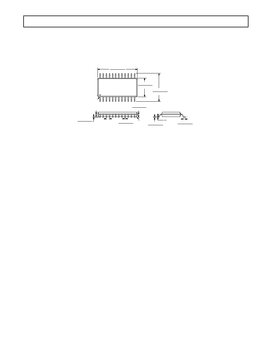
REV. 0
ADT7463
49
OUTLINE DIMENSIONS
24-Lead SOIC, 0.025 Lead Pitch [QSOP]
(RQ-24)
Dimensions shown in millimeters and inches
24
13
12
1
8.74 (0.3341)
8.56 (0.3370)
6.20 (0.2441)
5.79 (0.2280)
PIN 1
3.99 (0.1571)
3.81 (0.1500)
SEATING
PLANE
0.25 (0.0098)
0.10 (0.0039)
0.30 (0.0118)
0.20 (0.0079)
0.64 (0.0252)
BSC
1.50 (0.0591)
MAX
1.75 (0.0689)
1.35 (0.0531)
0.20 (0.0079)
0.18 (0.0071)
1.27 (0.0500)
0.41 (0.0161)
8
0
CONTROLLING DIMENSIONS ARE IN MILLIMETERS; INCH DIMENSIONS
(IN PARENTHESES) ARE ROUNDED-OFF MILLIMETER EQUIVALENTS FOR
REFERENCE ONLY AND ARE NOT APPROPRIATE FOR USE IN DESIGN

50

51

C03196011/02(0)
PRINTED IN U.S.A.
52

This datasheet has been download from:
www.datasheetcatalog.com
Datasheets for electronics components.
Document Outline