 | ÐлекÑÑоннÑй компоненÑ: ADT7516 | СкаÑаÑÑ:  PDF PDF  ZIP ZIP |
Äîêóìåíòàöèÿ è îïèñàíèÿ www.docs.chipfind.ru

SPI/I
2
C Compatible, Temperature Sensor,
4-Channel ADC and Quad Voltage Output DAC
ADT7516/ADT7517/ADT7519
Rev. A
Information furnished by Analog Devices is believed to be accurate and reliable.
However, no responsibility is assumed by Analog Devices for its use, nor for any
infringements of patents or other rights of third parties that may result from its use.
Specifications subject to change without notice. No license is granted by implication
or otherwise under any patent or patent rights of Analog Devices. Trademarks and
registered trademarks are the property of their respective owners.
One Technology Way, P.O. Box 9106, Norwood, MA 02062-9106, U.S.A.
Tel: 781.329.4700
www.analog.com
Fax: 781.326.8703
© 2004 Analog Devices, Inc. All rights reserved.
FEATURES
ADT7516--four 12-bit DACs
ADT7517--four 10-bit DACs
ADT7519--four 8-bit DACs
Buffered voltage output
Guaranteed monotonic by design over all codes
10-bit temperature-to-digital converter
10-bit 4-channel ADC
DC input bandwidth
Input range: 0 V to 2.28 V
Temperature range: 40°C to +120°C
Temperature sensor accuracy of typ: ±0.5°C
Supply range: 2.7 V to 5.5 V
DAC output range: 0 V to 2 V
REF
Power-down current: 1 µA
Internal 2.28 V
REF
option
Double-buffered input logic
Buffered reference input
Power-on reset to 0 V DAC output
Simultaneous update of outputs (LDAC function)
On-chip rail-to-rail output buffer amplifier
SPI
®
, I
2
C
®
, QSPITM, MICROWIRETM, and DSP compatible
4-wire serial interface
SMBus packet error checking (PEC) compatible
16-lead QSOP package
APPLICATIONS
Portable battery-powered instruments
Personal computers
Smart battery chargers
Telecommunications systems
Electronic text equipment
Domestic appliances
Process control
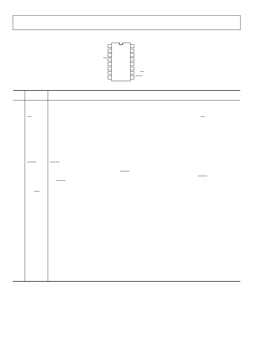
PIN CONFIGURATION
ADT7516/
ADT7517/
ADT7519
TOP VIEW
(Not to Scale)
V
OUT
-B
1
V
OUT
-C
16
V
OUT
-A
2
V
OUT
-D
15
V
REF
-IN
3
AIN4
14
CS
4
SCL/SCLK
13
GND
5
SDA/DIN
12
V
DD
6
DOUT/ADD
11
D+/AIN1
7
INT/INT
10
D/AIN2
8
LDAC/AIN3
9
02883-A
-
006
Figure 1.
GENERAL DESCRIPTION
The ADT7516/ADT7517/ADT7519
1
combine a 10-bit temp-
erature-to-digital converter, a 10-bit 4-channel ADC, and a
quad 12-/10-/8-bit DAC, respectively, in a 16-lead QSOP
package. The parts also include a band gap temperature sensor
and a 10-bit ADC to monitor and digitize the temperature
reading to a resolution of 0.25°C.
The ADT7516/ADT7517/ ADT7519 operate from a single 2.7 V
to 5.5 V supply. The input voltage range on the ADC channels is
0 V to 2.28 V, and the input bandwidth is dc. The reference for
the ADC channels is derived internally. The output voltage of
the DAC ranges from 0 V to V
DD
, with an output voltage settling
time of 7 ms typical.
The ADT7516/ADT7517/ADT7519 provide two serial interface
options: a 4-wire serial interface that is compatible with SPI,
QSPI, MICROWIRE, and DSP interface standards, and a 2-wire
SMBus/I
2
C interface. They feature a standby mode that is
controlled through the serial interface.
The reference for the four DACs is derived either internally or
from a reference pin. The outputs of all DACs may be updated
simultaneously using the software LDAC function or the
external LDAC pin. The ADT7516/ADT7517/ADT7519
incorporate a power-on reset circuit, which ensures that the
DAC output powers up to 0 V and remains there until a valid
write takes place.
The ADT7516/ADT7517/ADT7519's wide supply voltage range,
low supply current, and SPI/I
2
C compatible interface make
them ideal for a variety of applications, including personal
computers, office equipment, and domestic appliances.
1
Protected by the following U.S. Patent Numbers: 6,169,442; 5,867,012;
5,764174. Other patents pending.

ADT7516/ADT7517/ADT7519
Rev. A | Page 2 of 44
TABLE OF CONTENTS
Specifications..................................................................................... 3
DAC AC Characteristics.............................................................. 6
Functional Block Diagram .............................................................. 8
Absolute Maximum Ratings............................................................ 9
ESD Caution.................................................................................. 9
Pin Configuration and Functional Descriptions........................ 10
Terminology .................................................................................... 11
Typical Performance Characteristics ........................................... 13
Theory of Operation ...................................................................... 19
Power-Up Calibration................................................................ 19
Conversion Speed....................................................................... 19
Function Description--Voltage Output.................................. 20
Functional Description--Analog Inputs................................. 23
ADC Transfer Function............................................................. 23
Functional Description--Measurement.................................. 25
ADT7516/ADT7517/ADT7519 Registers............................... 28
Serial Interface ............................................................................ 37
SMBus Alert Response............................................................... 43
Outline Dimensions ....................................................................... 44
Ordering Guide .......................................................................... 44
REVISION HISTORY
8/04--Data Sheet Changed from Rev. 0 to Rev. A
Updated Format...................................................................... Universal
Deleted ADT7518
Added ADT7519..................................................................... Universal
Change to Internal V
REF
Value..............................................................5
Change to Equation.............................................................................26
7/03--Initial Version: Rev. 0

ADT7516/ADT7517/ADT7519
Rev. A | Page 3 of 44
SPECIFICATIONS
Table 1. Temperature range is as follows: A version: 40°C to +120°C. V
DD
= 2.7 V to 5.5 V, GND = 0 V, REF
IN
= 2.25 V, unless
otherwise noted.
Parameter
1
Min
Typ
Max
Unit
Conditions/Comments
DAC DC PERFORMANCE
2, 3
ADT7519
Resolution
8
Bits
Relative Accuracy
±0.15
±1
LSB
Differential Nonlinearity
±0.02
±0.25
LSB
Guaranteed monotonic over all codes.
ADT7517
Resolution
10
Bits
Relative Accuracy
±0.5
±4
LSB
Differential Nonlinearity
±0.05
±0.5
LSB
Guaranteed monotonic over all codes.
ADT7516
Resolution
12
Bits
Relative Accuracy
±2
±16
LSB
Differential Nonlinearity
±0.02
±0.9
LSB
Guaranteed monotonic over all codes.
Offset Error
±0.4
±2
% of FSR
Gain Error
±0.3
±2
% of FSR
Lower Deadband
20
65
mV
Lower deadband exists only if offset error is
negative. See Figure 8.
Upper Deadband
60
100
mV
Upper deadband exists if V
REF
= V
DD
and off-set
plus gain error is positive. See Figure 9.
Offset Error Drift
4
12
ppm of FSR/°C
Gain Error Drift
4
5
ppm of FSR/°C
DC Power Supply Rejection
Ratio
4
60
dB
V
DD
= ±10%.
DC Crosstalk
4
200
µV
See Figure 5.
ADC DC ACCURACY
Max V
DD
= 5 V.
Resolution
10 Bits
Total Unadjusted Error (TUE)
2
3
% of FSR
Offset Error
±0.5
% of FSR
Gain Error
±2
% of FSR
ADC
BANDWIDTH
DC Hz
ANALOG
INPUTS
Input Voltage Range
0
2.28
V
AIN1 to AIN4. C4 = 0 in Control Configuration 3.
0
V
DD
V
AIN1 to AIN4. C4 = 0 in Control Configuration 3.
DC Leakage Current
±1
µA
Input Capacitance
5
20
pF
Input Resistance
10
M
THERMAL CHARACTERISTICS
INTERNAL TEMPERATURE SENSOR
Internal reference used. Averaging on.
Accuracy @ V
DD
= 3.3 V ±10%
±1.5
°C
T
A
= 85°C.
±0.5
±3
°C
T
A
= 0°C to +85°C.
±2
±5
°C
T
A
= 40°C to +120°C.
Accuracy @ V
DD
= 5 V ±5%
±2
±3
°C
T
A
= 0°C to +85°C.
±3
±5
°C
T
A
= 40°C to +120°C.
Resolution
10
Bits
Equivalent to 0.25°C.
Long-Term Drift
0.25
°C
Drift over 10 years if part is operated at 55°C.

ADT7516/ADT7517/ADT7519
Rev. A | Page 4 of 44
Parameter
1
Min
Typ
Max
Unit
Conditions/Comments
THERMAL CHARACTERISTICS
EXTERNAL TEMPERATURE SENSOR
External transistor = 2N3906.
Accuracy @ V
DD
= 3.3 V ±10%
±1.5
°C
T
A
= 85°C.
±3
°C
T
A
= 0°C +85°C.
±5
°C
T
A
= 40°C to +120°C.
Accuracy @ V
DD
= 5 V ±5%
±2
±3
°C
T
A
= 0°C +85°C.
±3
±5
°C
T
A
= 40°C to +120°C.
Resolution
10 Bits
Equivalent
to
0.25°C.
Output Source Current
180
µA
High Level.
11
µA
Low
Level.
Thermal Voltage Output
8-Bit DAC Output
Resolution 1
°C
Scale Factor
8.97
mV/°C
0 V to V
REF
output. T
A
= 40°C to +120°C.
17.58
mV/°C
0 V to 2 V
REF
output. T
A
= 40°C to +120°C.
10-Bit DAC Output
Resolution 0.25
°C
Scale Factor
2.2
mV/°C
0 V to V
REF
output. T
A
= 40°C to +120°C.
4.39
mV/°C
0 V to 2 V
REF
output. T
A
= 40°C to +120°C.
CONVERSION
TIMES
Single
channel
mode.
Slow
ADC
V
DD
/AIN
11.4
ms
Averaging (16 samples) on.
712
µs
Averaging
off.
Internal Temperature
11.4
ms
Averaging (16 samples) on.
712
µs
Averaging
off.
External Temperature
24.22
ms
Averaging (16 samples) on.
1.51
ms
Averaging
off.
Fast
ADC
V
DD
/AIN
712
µs
Averaging (16 samples) on.
44.5
µs
Averaging
off.
Internal Temperature
2.14
ms
Averaging (16 samples) on.
134
µs
Averaging
off.
External Temperature
14.25
ms
Averaging (16 samples) on.
890
µs
Averaging
off.
ROUND ROBIN UPDATE RATE
5
Slow ADC @ 25°C
Time to complete one measurement cycle
through all channels.
Averaging On
79.8
ms
AIN1 and AIN2 are selected on Pins 7 and 8.
Averaging Off
4.99
ms
AIN1 and AIN2 are selected on Pins 7 and 8.
Averaging On
94.76
ms
D+ and D are selected on Pins 7 and 8.
Averaging Off
9.26
ms
D+ and D- are selected on Pins 7 and 8.
Fast ADC @ 25°C
Averaging On
6.41
ms
AIN1 and AIN2 are selected on Pins 7 and 8.
Averaging Off
400.84
µs
AIN1 and AIN2 are selected on Pins 7 and 8.
Averaging On
21.77
ms
D+ and D are selected on Pins 7 and 8.
Averaging Off
3.07
ms
D+ and D are selected on Pins 7 and 8.
DAC EXTERNAL REFERENCE INPUT
4
V
REF
Input Range
1
V
DD
V Buffered
reference.
V
REF
Input Impedance
>10
M
Buffered reference and power-down mode.
Reference Feedthrough
90
dB
Frequency = 10 kHz.
Channel-to-Channel Isolation
75
dB
Frequency = 10 kHz.
ADT7516/ADT7517/ADT7519
Rev. A | Page 5 of 44
Parameter
1
Min
Typ
Max
Unit
Conditions/Comments
ON-CHIP
REFERENCE
Reference Voltage
4
2.28
V
Temperature Coefficient
4
80
ppm/°C
OUTPUT CHARACTERISTICS
4
Output Voltage
6
0.001
V
DD
- 0.1
V
This is a measure of the minimum and maximum
drive capability of the output amplifier.
DC Output Impedance
0.5
Short Circuit Current
25
mA
V
DD
= 5 V.
16
mA
V
DD
= 3 V.
Power-Up Time
2.5
µs
Coming out of power-down mode. V
DD
= 5 V.
5
µs
Coming out of power-down mode. V
DD
= 3.3 V.
DIGITAL INPUTS
4
Input
Current
±1 µA
V
IN
= 0 V to V
DD.
V
IL
, Input Low Voltage
0.8
V
V
IH
, Input High Voltage
1.89
V
Pin Capacitance
3
10
pF
All digital inputs.
SCL, SDA Glitch Rejection
50
ns
Input filtering suppresses noise spikes of less
than 50 ns.
LDAC Pulse Width
20
ns
Edge triggered input.
DIGITAL
OUTPUT
Digital High Voltage, V
OH
2.4
V
I
SOURCE
= I
SINK
= 200 µA.
Output Low Voltage, V
OL
0.4 V
I
OL
= 3 mA.
Output High Current, I
OH
1
mA
V
OH
= 5 V.
Output Capacitance, C
OUT
50 pF
INT/INT Output Saturation Voltage 0.8 V
I
OUT
= 4 mA.
I
2
C TIMING CHARACTERISTICS
7,
8
Serial Clock Period, t
1
2.5
µs
Fast Mode I
2
C. See Figure 2.
Data In Setup Time to SCL High, t
2
50
ns
Data Out Stable after SCL Low, t
3
0
ns
See Figure 2.
SDA Low Setup Time to SCL
Low (Start Condition), t
4
50
ns
See Figure 2.
SDA High Hold Time after SCL
High (Stop Condition), t
5
50
ns
See Figure 2.
SDA and SCL Fall Time, t
6
90 ns
See
Figure
2.
SPI TIMING CHARACTERISTICS
4
,
9
CS to SCLK Setup Time, t
1
0
ns
See Figure 3.
SCLK High Pulse Width, t
2
50
ns
See Figure 3.
SCLK Low Pulse Width, t
3
50
ns
See Figure 3.
Data Access Time after SCLK
Falling Edge, t
4
,
10
35 ns
Data Setup Time Prior to SCLK
Rising Edge, t
5
20
ns
See Figure 3.
Data Hold Time after SCLK Rising
Edge, t
6
0
ns
See Figure 3.
CS to SCLK Hold Time, t
7
0
µs
See Figure 3.
CS to DOUT High Impedance, t
8
40
ns
See Figure 3.
ADT7516/ADT7517/ADT7519
Rev. A | Page 6 of 44
Parameter
1
Min
Typ
Max
Unit
Conditions/Comments
POWER REQUIREMENTS
V
DD
2.7
5.5
V
V
DD
Settling Time
50
ms
V
DD
settles to within 10% of its final voltage level.
I
DD
(Normal Mode)
11
3
mA
V
DD
= 3.3 V, V
IH
= V
DD
, and V
IL
= GND.
2.2
3
mA
V
DD
= 5 V, V
IH
= V
DD
, and V
IL
= GND.
I
DD
(Power-Down Mode)
10
µA
V
DD
= 3.3 V, V
IH
= V
DD
, and V
IL
= GND.
10 µA
V
DD
= 5 V, V
IH
= V
DD
, and V
IL
= GND.
Power
Dissipation
10 mW
V
DD
= 3.3 V. Normal mode.
33 µW
V
DD
= 3.3 V. Shutdown mode.
1
See the
section.
Terminology
2
DC specifications are tested with the outputs unloaded.
3
Linearity is tested using a reduced code range: ADT7516 (Code 115 to 4095); ADT7517 (Code 28 to 1023); ADT7519 (Code 8 to 255).
4
Guaranteed by design and characterization, not production tested.
5
Round robin is the continuous sequential measurement of the following channels: V
DD
, internal temperature, external temperature (AIN1, AIN2), AIN3, and AIN4.
6
For the amplifier output to reach its minimum voltage, the offset error must be negative. For the amplifier output to reach its maximum voltage (V
REF
= V
DD
), the offset
plus gain error must be positive.
7
The SDA and SCL timing is measured with the input filters turned on to meet the fast-mode I
2
C specification. Switching off the input filters improves the transfer rate
but has a negative effect on the EMC behavior of the part.
8
Guaranteed by design, not production tested.
9
All input signals are specified with tr = tf = 5 ns (10% to 90% of V
DD
), and timed from a voltage level of 1.6 V.
10
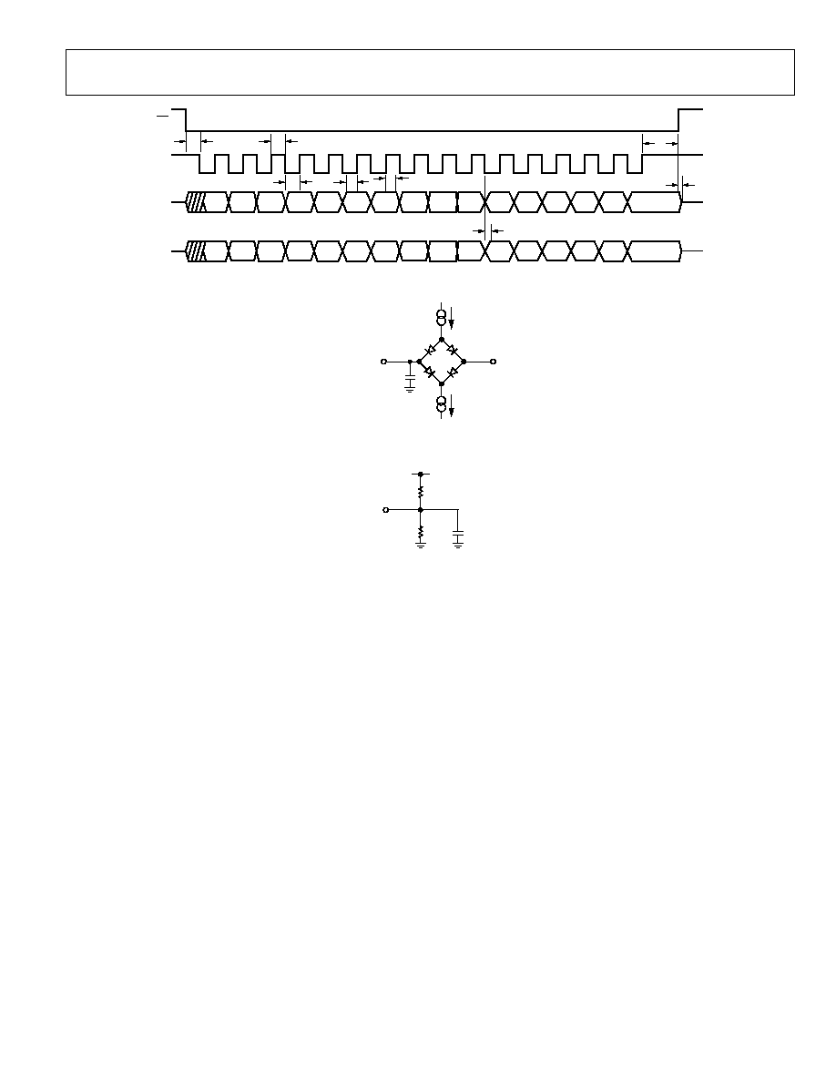
Measured with the load circuit shown in Figure 4.
11
The I
DD
specification is valid for all DAC codes and full-scale analog input voltages. Interface inactive. All DACs and ADCs active. Load currents excluded.
DAC AC CHARACTERISTICS
Table 2. V
DD
= 2.7 V to 5.5 V, R
L
= 4.7 k to GND; C
L
= 200 pF to GND; 4.7 k to V
DD
; all specifications T
MIN
to T
MAX
, unless
otherwise noted.
Parameter
1, 2
Min
Typ
3
Max
Unit
Conditions/Comments
Output Voltage Settling Time
V
REF
= V
DD
= 5 V.
ADT7519
6
8
µs
1/4 scale to 3/4 scale change (40h to C0h).
ADT7517
7
9
µs
1/4 scale to 3/4 scale change (100h to 300h).
ADT7516
8
10
µs
1/4 scale to 3/4 scale change (400h to C00h).
Slew Rate
0.7
V/µs
Major-Code Change Glitch Energy
12
nV-s
1 LSB change around major carry.
Digital Feedthrough
0.5
nV-s
Digital Crosstalk
1
nV-s
Analog Crosstalk
0.5
nV-s
DAC-to-DAC Crosstalk
3
nV-s
Multiplying Bandwidth
200
kHz
V
REF
= 2 V ±0.1 V p-p.
Total Harmonic Distortion
70
dB
V
REF
= 2.5 V ±0.1 V p-p. Frequency = 10 kHz.
1
See
section.
Terminology
2
Guaranteed by design and characterization, not production tested.
3
@ 25°C.
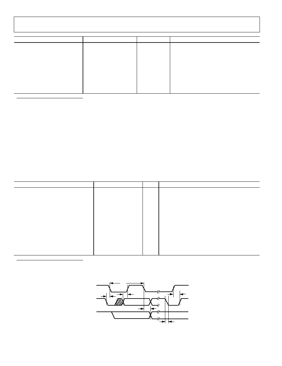
SCL
t
4
t
2
t
1
t
3
t
5
t
6
SDA
DATA IN
SDA
DATA OUT
02883-A
-
002
Figure 2. I
2
C Bus Timing Diagram
ADT7516/ADT7517/ADT7519
Rev. A | Page 7 of 44
t
1
t
2
t
3
t
5
t
6
t
4
t
7
t
8
D7
CS
SCLK
DIN
DOUT
D6
D5
D4
D3
D2
D1
D0
X
X
X
X
X
X
X
X
X
X
X
X
X
X
X
X
D7
D6
D5
D4
D3
D2
D1
D0
02883-A
-
003
Figure 3. SPI Bus Timing Diagram
200
µ
A
I
OH
1.6V
TO OUTPUT
PIN
C
L
50pF
200
µ
A
I
OL
02883-A
-
004
Figure 4. Load Circuit for Access Time and Bus Relinquish Time
4.7k
4.7k
V
DD
TO DAC
OUTPUT
200pF
02883-A
-
005
Figure 5. Load Circuit for DAC Outputs
ADT7516/ADT7517/ADT7519
Rev. A | Page 8 of 44
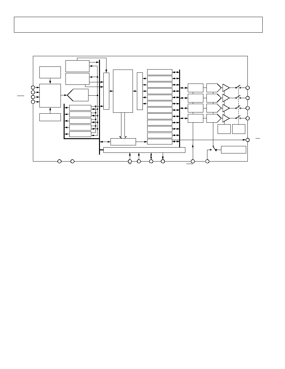
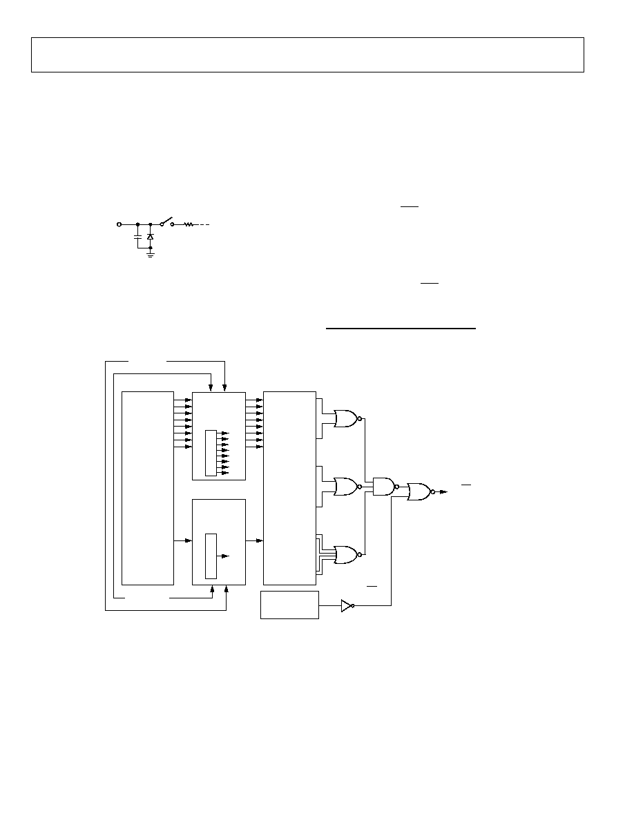
FUNCTIONAL BLOCK DIAGRAM
7
D+/AIN1
8
D/AIN2
9
LDAC/AIN3
14
AIN4
AIN4
VALUE REGISTER
AIN3
VALUE REGISTER
AIN2
VALUE REGISTER
AIN1
VALUE REGISTER
VDD
VALUE REGISTER
12
SDA
13
SCL
5
GND
6
V
DD
11
ADD
9
LDAC/AIN3
3
V
REF
-IN
4
CS
ADDRESS POINTER
REGISTER
DI
GI
TAL MUX
DI
GI
TAL MUX
T
HIGH
LIMIT
REGISTERS
LIMIT
COMPARATOR
T
LOW
LIMIT
REGISTERS
V
CC
LIMIT
REGISTERS
AIN
HIGH
LIMIT
REGISTERS
AIN
LOW
LIMIT
REGISTERS
CONTROL CONFIG. 1
REGISTER
CONTROL CONFIG. 2
REGISTER
CONTROL CONFIG. 3
REGISTER
DAC CONFIGURATION
REGISTERS
LDAC CONFIGURATION
REGISTERS
INTERRUPT MASK
REGISTERS
STATUS
REGISTERS
ON-CHIP
TEMPERATURE
SENSOR
INTERNAL
TEMPERATURE
VALUE REGISTER
EXTERNAL
TEMPERATURE
VALUE REGISTER
V
DD
SENSOR
ADT7516/ADT7517/ADT7519
ANALOG
MUX
STRING
DAC A
A-TO-D
CONVERTER
2
DAC A
REGISTERS
STRING
DAC B
1
DAC B
REGISTERS
STRING
DAC C
16
DAC C
REGISTERS
STRING
DAC D
15
V
OUT
-A
V
OUT
-B
V
OUT
-C
V
OUT
-D
INT/INT
DAC D
REGISTERS
POWER-
DOWN
LOGIC
GAIN
SELECT
LOGIC
INTERNAL
REFERENCE
SPI/SMBus INTERFACE
10
02883-A
-
001
Figure 6.
ADT7516/ADT7517/ADT7519
Rev. A | Page 9 of 44
ABSOLUTE MAXIMUM RATINGS
Table 3.
Parameter Rating
V
DD
to GND
0.3 V to +7 V
Analog Input Voltage to GND
0.3 V to V
DD
+ 0.3 V
Digital Input Voltage to GND
0.3 V to V
DD
+ 0.3 V
Digital Output Voltage to GND
0.3 V to V
DD
+ 0.3 V
Reference Input Voltage to GND
0.3 V to V
DD
+ 0.3 V
Operating Temperature Range
40°C to +120°C
Storage Temperature Range
65°C to +150°C
Junction Temperature
150°C
16-Lead QSOP Package
Power Dissipation
1
(T
J
max T
A
)/
JA
Thermal Impedance
2
JA
Junction-to-Ambient 105.44°C/W
JC
Junction-to-Case 38.8°C/W
IR Reflow Soldering
Peak Temperature
220°C (0°C/5°C)
Time at Peak Temperature
10 sec to 20 sec
Ramp-Up Rate
2°C/sec to 3°C/sec
Ramp-Down Rate
6°C/sec
Table 4. I
2
C Address Selection
ADD Pin
I
2
C Address
Low
1001 000
Float
1001 010
High
1001 011
Stresses above those listed under Absolute Maximum Ratings
may cause permanent damage to the device. This is a stress
rating only; functional operation of the device at these or any
other conditions above those indicated in the operational
section of this specification is not implied. Exposure to absolute
maximum rating conditions for extended periods may affect
device reliability.
1
Values relate to package being used on a 4-layer board.
2
Junction-to-case resistance is applicable to components featuring a
preferential flow direction, e.g., components mounted on a heat sink.
Junction-to-ambient resistance is more useful for air cooled PCB-mounted
components.
ESD CAUTION
ESD (electrostatic discharge) sensitive device. Electrostatic charges as high as 4000 V readily accumulate on
the human body and test equipment and can discharge without detection. Although this product features
proprietary ESD protection circuitry, permanent damage may occur on devices subjected to high energy
electrostatic discharges. Therefore, proper ESD precautions are recommended to avoid performance
degradation or loss of functionality.
ADT7516/ADT7517/ADT7519
Rev. A | Page 10 of 44
PIN CONFIGURATION AND FUNCTIONAL DESCRIPTIONS
ADT7516/
ADT7517/
ADT7519
TOP VIEW
(Not to Scale)
V
OUT
-B
1
V
OUT
-C
16
V
OUT
-A
2
V
OUT
-D
15
V
REF
-IN
3
AIN4
14
CS
4
SCL/SCLK
13
GND
5
SDA/DIN
12
V
DD
6
DOUT/ADD
11
D+/AIN1
7
INT/INT
10
D/AIN2
8
LDAC/AIN3
9
02883-A
-
006
Figure 7. Pin Configuration (QSOP Package)
Table 5. Pin Function Descriptions
Pin
No.
Mnemonic Description
1
V
OUT
-B
Buffered Analog Output Voltage from DAC B. The output amplifier has rail-to-rail operation.
2
V
OUT
-A
Buffered Analog Output Voltage from DAC A. The output amplifier has rail-to-rail operation.
3
V
REF
-IN
Reference Input Pin for All Four DACs. This input is buffered and has an input range from 1 V to V
DD
.
4
CS
SPI Active Low Control Input. This is the frame synchronization signal for the input data. When CS goes low, it enables
the input register, and data is transferred in on the rising edges and out on the falling edges of the subsequent serial
clocks. It is recommended that this pin be tied high to V
DD
when operating the serial interface in I
2
C mode. -
5
GND
Ground Reference Point for All Circuitry on the Part. Analog and digital ground.
6
V
DD
Positive Supply Voltage, 2.7 V to 5.5 V. The supply should be decoupled to ground.
7
D+/AIN1
D+. Positive Connection to External Temperature Sensor.
AIN1. Analog Input. Single-ended analog input channel. Input range is 0 V to 2.28 V or 0 V to V
DD
.
8
D/AIN2
D. Negative Connection to External Temperature Sensor.
AIN2. Analog Input. Single-ended analog input channel. Input range is 0 V to 2.28 V or 0 V to V
DD
.
9
LDAC/AIN3 LDAC. Active Low Control Input. Transfers the contents of the input registers to their respective DAC registers. A
falling edge on this pin forces any or all DAC registers to be updated if the input registers have new data. A minimum
pulse width of 20 ns must be applied to the LDAC pin to ensure proper loading of a DAC register. This allows simul-
taneous update of all DAC outputs. Bit C3 of the Control Configuration 3 register enables the LDAC pin. Default is with
the LDAC pin controlling the loading of the DAC registers.
AIN3. Analog Input. Single-ended analog input channel. Input range is 0 V to 2.28 V or 0 V to V
DD
.
10
INT/INT
Over Limit Interrupt. The output polarity of this pin can be set to give an active low or active high interrupt when
temperature,V
DD
, or AIN limits are exceeded. The default is active low. Open-drain output--needs a pull-up resistor.
11
DOUT/ADD SPI Serial Data Output. Logic output. Data is clocked out of any register at this pin. Data is clocked out on the falling
edge of SCLK. Open-drain output--needs a pull-up resistor.
ADD. I
2
C Serial Bus Address Selection Pin. Logic input. A low on this pin gives the address 1001 000; leaving it floating
gives the address 1001 010; and setting it high gives the address 1001 011. The I
2
C address set up by the ADD pin is
not latched by the device until after this address has been sent twice. On the eighth SCL cycle of the second valid
communication, the serial bus address is latched in. Any subsequent changes on this pin will have no effect on the I
2
C
serial bus address.
12
SDA/DIN
SDA. I
2
C Serial Data Input/Output. I
2
C serial data to be loaded into the part's registers and read from these registers is
provided on this pin. Open-drain configuration--needs a pull-up resistor.
DIN. SPI Serial Data Input. Serial data to be loaded into the part's registers is provided on this pin. Data is clocked into
a register on the rising edge of SCLK. Open-drain configuration--needs a pull-up resistor.
13
SCL/SCLK
Serial Clock Input. This is the clock input for the serial port. The serial clock is used to clock data out of any register of
the ADT7516/ADT7517/ADT7519 and also to clock data into any register that can be written to. Open-drain
configuration--needs a pull-up resistor.
14
AIN4
Analog Input. Single-ended analog input channel. Input range is 0 V to 2.28 V or 0 V to V
DD
.
15
V
OUT
-D
Buffered Analog Output Voltage from DAC D. The output amplifier has rail-to-rail operation.
16
V
OUT
-C
Buffered Analog Output Voltage from DAC C. The output amplifier has rail-to-rail operation.

ADT7516/ADT7517/ADT7519
Rev. A | Page 11 of 44
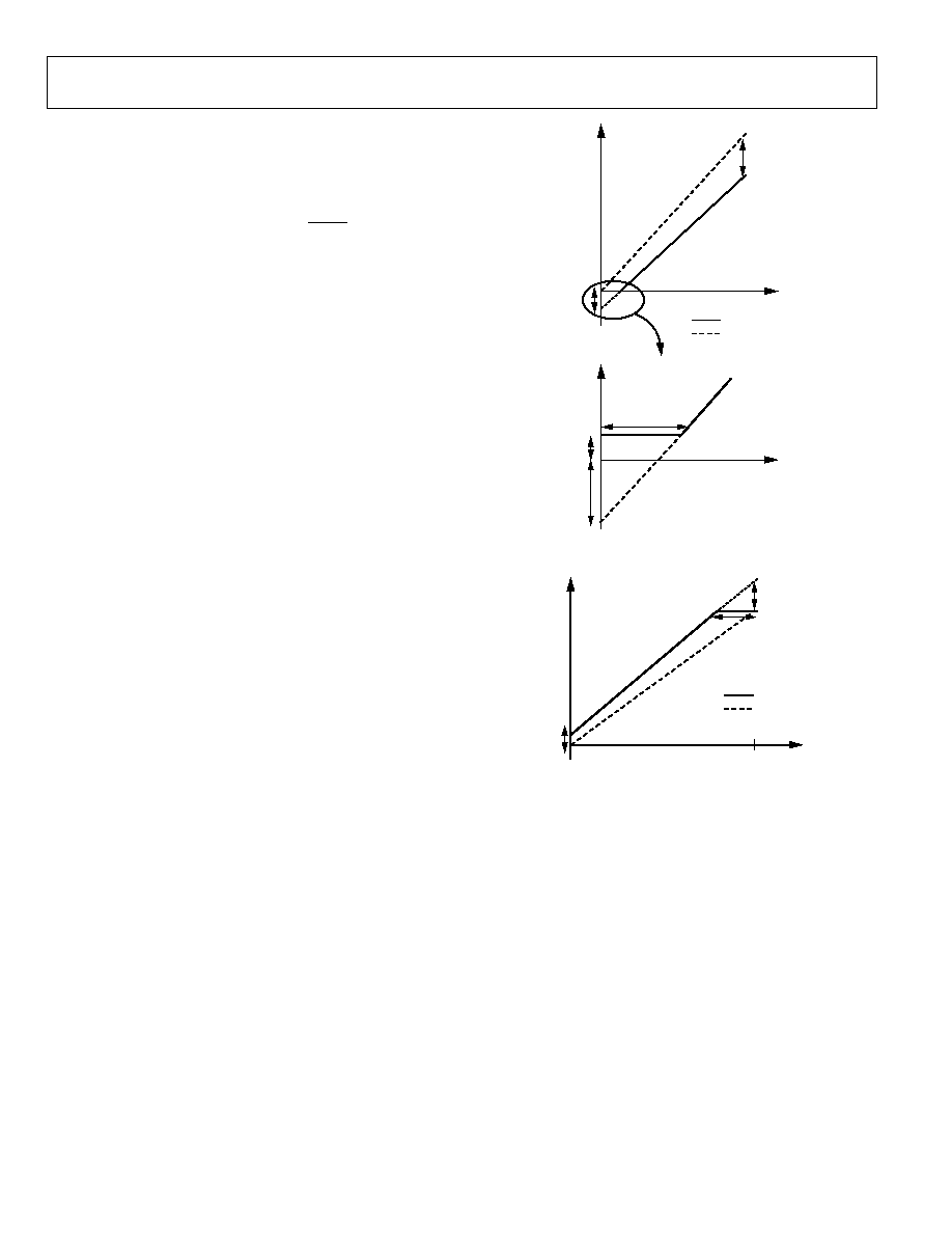
TERMINOLOGY
Relative Accuracy
Relative accuracy or integral nonlinearity (INL) is a measure of
the maximum deviation, in LSBs, from a straight line passing
through the endpoints of the transfer function. Typical INL
versus code plots can be seen in Figure 10, Figure 11, and
Figure 12.
Differential Nonlinearity
Differential nonlinearity (DNL) is the difference between the
measured change and the ideal 1 LSB change between any two
adjacent codes. A specified differential nonlinearity of ±0.9 LSB
maximum ensures monotonicity. Typical DAC DNL versus code
plots can be seen in Figure 13, Figure 14, and Figure 15.
Total Unadjusted Error (TUE)
Total unadjusted error is a comprehensive specification that
includes the sum of the relative accuracy error, gain error, and
offset error under a specified set of conditions.
Offset Error
This is a measure of the offset error of the DAC and the output
amplifier (See Figure 8 and Figure 9). It can be negative or
positive, and it is expressed in mV.
Offset Error Match
This is the difference in offset error between any two channels.
Gain Error
This is a measure of the span error of the DAC. It is the
deviation in slope of the actual DAC transfer characteristic
from the ideal expressed as a percentage of the full-scale range.
Gain Error Match
This is the difference in gain error between any two channels.
Offset Error Drift
This is a measure of the change in offset error with changes in
temperature. It is expressed in (ppm of full-scale range)/°C.
Gain Error Drift
This is a measure of the change in gain error with changes in
temperature. It is expressed in (ppm of full-scale range)/°C.
Long Term Temperature Drift
This is a measure of the change in temperature error with the
passage of time. It is expressed in °C. The concept of long-term
stability has been used for many years to describe the amount
an IC's parameter would shift during its lifetime. This is a
concept that has typically been applied to both voltage
references and monolithic temperature sensors. Unfortunately,
integrated circuits cannot be evaluated at room temperature
(25°C) for 10 years or so to determine this shift. Manufacturers
perform accelerated lifetime testing of integrated circuits by
operating ICs at elevated temperatures (between 125°C and
150°C) over a shorter period (typically between 500 and 1000
hours). As a result, the lifetime of an integrated circuit is
significantly accelerated due to the increase in rates of reaction
within the semiconductor material.
DC Power Supply Rejection Ratio (PSRR)
This indicates how the output of the DAC is affected by changes
in the supply voltage. PSRR is the ratio of the change in V
OUT
to
a change in V
DD
for full-scale output of the DAC. It is measured
in dB. V
REF
is held at 2 V and V
DD
is varied ±10%.
DC Crosstalk
This is the dc change in the output level of one DAC in response
to a change in the output of another DAC. It is measured with a
full-scale output change on one DAC while monitoring another
DAC. It is expressed in µV.
Reference Feedthrough
This is the ratio of the amplitude of the signal at the DAC
output to the reference input when the DAC output is not being
updated (i.e., LDAC is high). It is expressed in dB.
Channel-to-Channel Isolation
This is the ratio of the amplitude of the signal at the output of
one DAC to a sine wave on the reference input of another DAC.
It is measured in dB.
Major-Code Transition Glitch Energy
Major-code transition glitch energy is the energy of the impulse
injected into the analog output when the code in the DAC
register changes state. It is normally specified as the area of the
glitch in nV-s and is measured when the digital code is changed
by 1 LSB at the major carry transition (011 . . . 11 to 100 . . . 00 or
100 . . . 00 to 011 . . . 11).
Digital Feedthrough
Digital feedthrough is a measure of the impulse injected into
the analog output of a DAC from the digital input pins of the
device but is measured when the DAC is not being written to. It
is specified in nV-s and is measured with a full-scale change on
the digital input pins, i.e., from all 0s to all 1s or vice versa.
Digital Crosstalk
This is the glitch impulse transferred to the output of one DAC
at midscale in response to a full-scale code change (all 0s to all
1s and vice versa) in the input register of another DAC. It is
measured in standalone mode and is expressed in nV-s.
Analog Crosstalk
This is the glitch impulse transferred to the output of one DAC
due to a change in the output of another DAC. It is measured by
loading one of the input registers with a full-scale code change
(all 0s to all 1s and vice versa) while keeping LDAC high. Then
pulse LDAC low and monitor the output of the DAC whose
digital code was not changed. The area of the glitch is expressed
in nV-s.
ADT7516/ADT7517/ADT7519
Rev. A | Page 12 of 44
DAC-to-DAC Crosstalk
This is the glitch impulse transferred to the output of one DAC
due to a digital code change and subsequent output change of
another DAC. This includes both digital and analog crosstalk. It
is measured by loading one of the DACs with a full-scale code
change (all 0s to all 1s and vice versa) with LDAC low and
monitoring the output of another DAC. The energy of the glitch
is expressed in nV-s.
Multiplying Bandwidth
The amplifiers within the DAC have a finite bandwidth. The
multiplying bandwidth is a measure of this. A sine wave on the
reference (with full-scale code loaded to the DAC) appears on
the output. The multiplying bandwidth is the frequency at
which the output amplitude falls to 3 dB below the input.
Total Harmonic Distortion
This is the difference between an ideal sine wave and its
attenuated version using the DAC. The sine wave is used as the
reference for the DAC, and the THD is a measure of the
harmonics present on the DAC output, expressed in dB.
Round Robin
This term is used to describe the ADT7516/ADT7517/
ADT7519 cycling through the available measurement channels
in sequence, taking a measurement on each channel.
DAC Output Settling Time
This is the time required, following a prescribed data change, for
the output of a DAC to reach and remain within ±0.5 LSB of the
final value. A typical prescribed change is from 1/4 scale to
3/4 scale.
AMPLIFIER
FOOTROOM
LOWER
DEADBAND
CODES
NEGATIVE
OFFSET
ERROR
GAIN ERROR
+
OFFSET ERROR
ACTUAL
OUTPUT
VOLTAGE
NEGATIVE
OFFSET
ERROR
DAC CODE
IDEAL
02883-A
-
007
Figure 8. DAC Transfer Function with Negative Offset
ACTUAL
GAIN ERROR
+
OFFSET ERROR
UPPER
DEADBAND
CODES
OUTPUT
VOLTAGE
POSITIVE
OFFSET
ERROR
DAC CODE
FULL SCALE
IDEAL
02883-A
-
008
Figure 9. DAC Transfer Function with Positive Offset (V
REF
= V
DD
)
ADT7516/ADT7517/ADT7519
Rev. A | Page 13 of 44
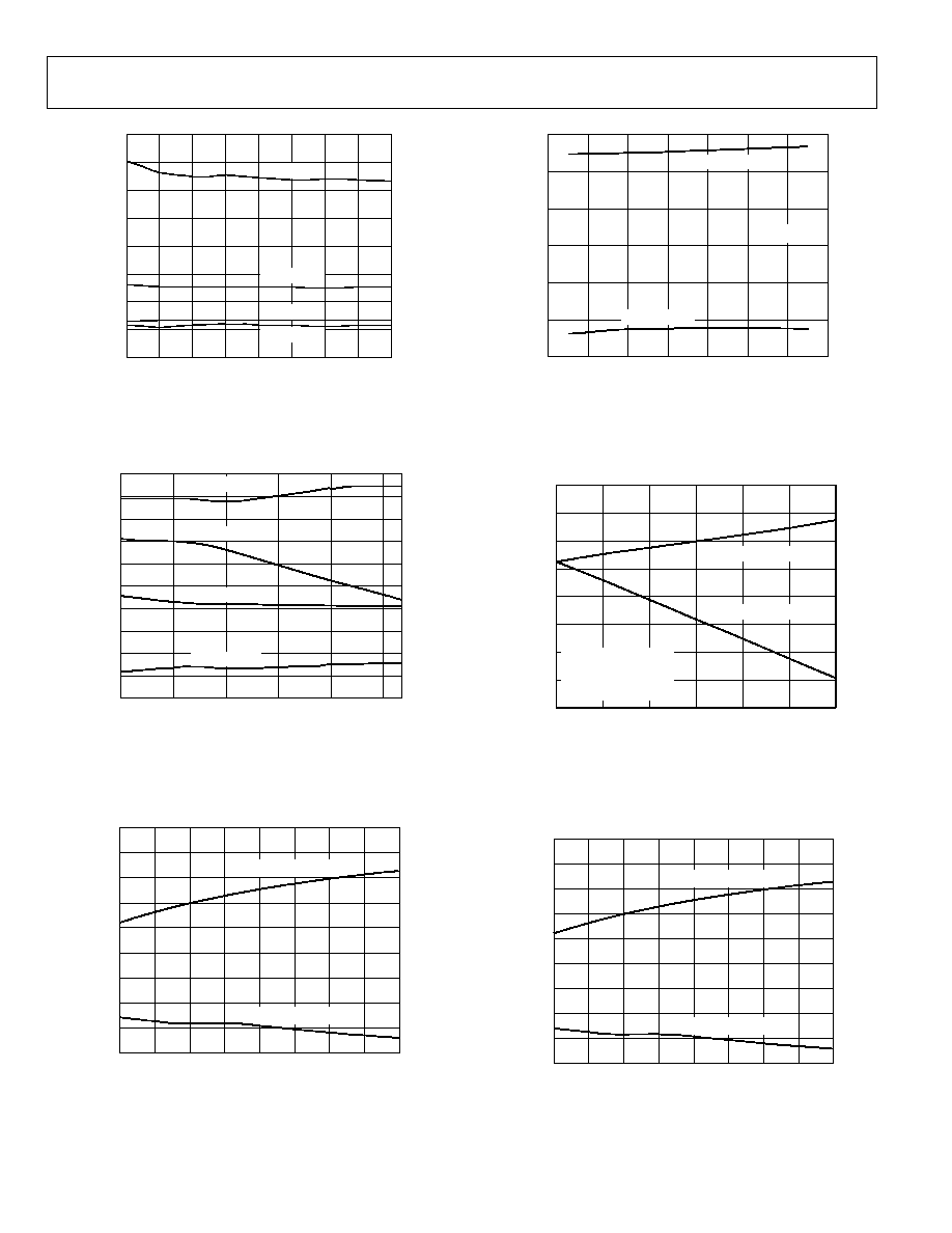
TYPICAL PERFORMANCE CHARACTERISTICS
0.20
0.15
0.10
0.05
0
0.05
INL E
RROR (LS
B
)
0.10
0.15
0.20
0
50
100
150
200
250
DAC CODE
02883-A
-
009
Figure 10. ADT7519 Typical DAC INL Plot
0.6
0
200
400
600
DAC CODE
INL E
RROR (LS
B
)
800
1000
0.6
0.4
0.2
0
0.2
0.4
02883-A
-
010
Figure 11. ADT7517 Typical DAC INL Plot
2000
1500
500
1000
0
2500
3000
3500 4000
DAC CODE
2.5
2.0
1.5
1.0
0.5
0
0.5
1.0
1.5
2.0
2.5
I
N
L E
RROR (LS
B
)
02883-A
-
011
Figure 12. ADT7516 Typical DAC INL Plot
0.10
0.08
0.06
0.04
0.02
0
0.02
0.04
0.06
0.08
0.10
DNL E
RROR (LS
B
)
0
50
100
150
200
250
DAC CODE
02883-A
-
012
Figure 13. ADT7519 Typical DAC DNL Plot
0.3
0.2
0.1
0
0.1
0.2
0.3
DNL E
RROR (LS
B
)
0
200
400
600
800
1000
DAC CODE
02883-A
-
013
Figure 14. ADT7517 Typical DAC DNL Plot
2000
1500
500
1000
0
2500
3000
3500 4000
DAC CODE
1.0
0.8
0.6
0.4
0.2
0
0.2
0.4
0.6
0.8
1.0
DNL E
RROR (LS
B
)
02883-A
-
014
Figure 15. ADT7516 Typical DAC DNL Plot
ADT7516/ADT7517/ADT7519
Rev. A | Page 14 of 44
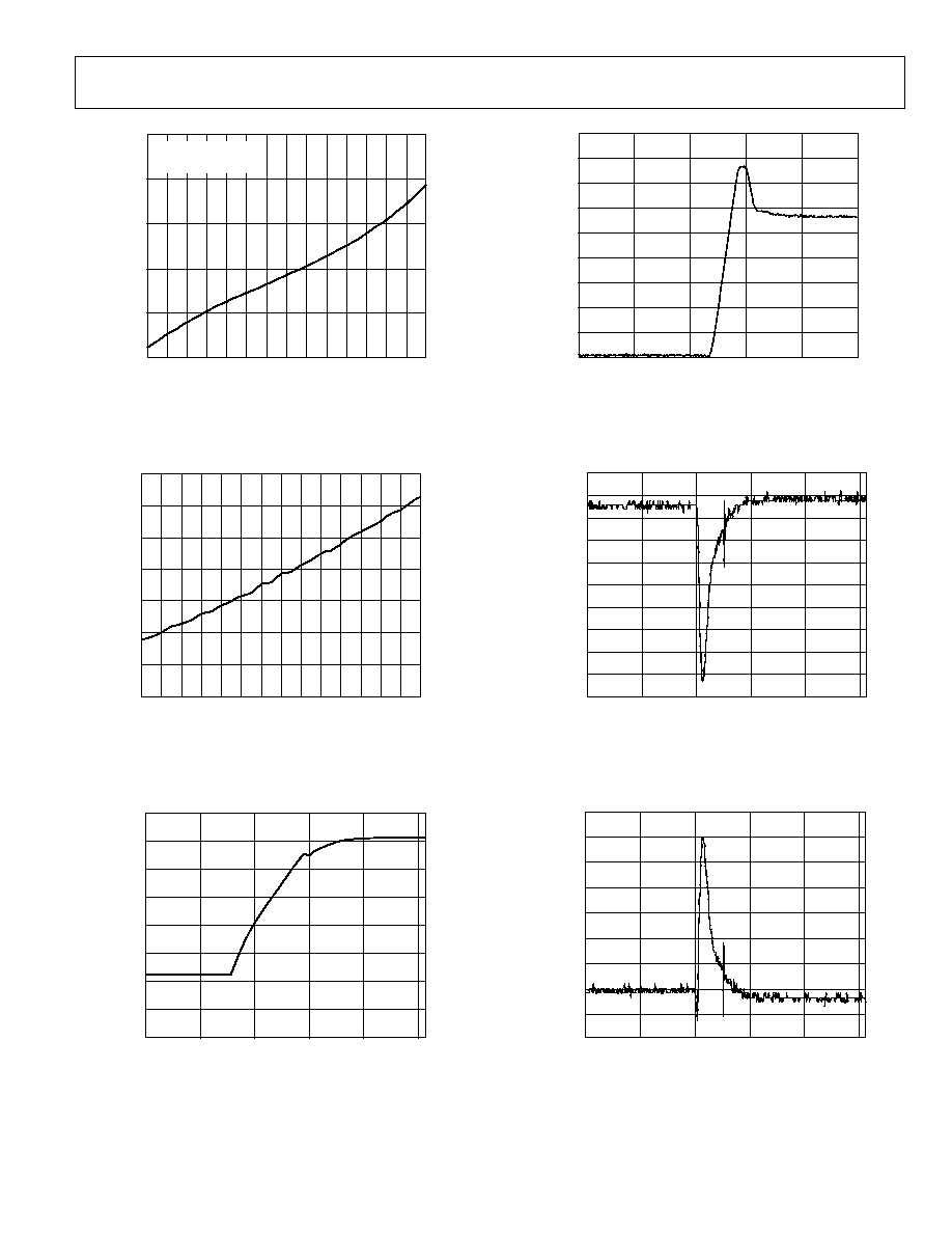
0.30
1.0
1.5
2.0
2.5
3.0
3.5
4.0
4.5
5.0
V
REF
(V)
E
RROR (LS
B
)
0.10
0.05
0
0.05
0.10
0.15
0.20
0.25
INL WCP
DNL WCP
DNL WCN
INL WCN
02883-A
-
015
Figure 16. ADT7519 DAC INL and DNL Error vs. V
REF
0.14
40
110
80
50
20
10
TEMPERATURE (
°
C)
E
RROR (LS
B
)
0.06
0.04
0.02
0
0.02
0.04
0.06
0.08
0.10
0.12
DNL WCN
INL WCP
INL WCN
DNL WCP
02883-A
-
016
Figure 17. ADT7519 DAC INL Error and DNL Error vs. Temperature
0
40
120
100
80
60
40
20
0
20
TEMPERATURE (
°
C)
E
RROR (LS
B
)
1.8
1.6
1.4
1.2
1.0
0.8
0.6
0.4
0.2
OFFSET ERROR
GAIN ERROR
02883-A
-
017
Figure 18. DAC Offset Error and Gain Error vs. Temperature
E
RROR (LS
B
)
20
15
10
5
0
5
10
2.7
3.3
3.6
4.0
V
DD
(V)
4.5
5.0
5.5
OFFSET ERROR
GAIN ERROR
V
REF
= 2.25V
02883-A
-
018
Figure 19. DAC Offset Error and Gain Error vs. V
DD
SOURCE CURRENT
SINK CURRENT
2.505
DAC OUTP
UT (V
)
2.465
2.470
2.475
2.480
2.485
2.490
2.495
2.500
0
1
2
3
CURRENT (mA)
4
5
6
V
DD
= 5V
V
REF
= 5V
DAC OUTPUT
LOADED TO MIDSCALE
0
2883-A
-
019
Figure 20. DAC V
OUT
Source and Sink Current Capability
0
40
120
100
80
60
40
20
0
20
TEMPERATURE (
°
C)
E
RROR (LS
B
)
1.8
1.6
1.4
1.2
1.0
0.8
0.6
0.4
0.2
OFFSET ERROR
GAIN ERROR
02883-A
-
017
Figure 21. Supply Current vs. DAC Code
ADT7516/ADT7517/ADT7519
Rev. A | Page 15 of 44
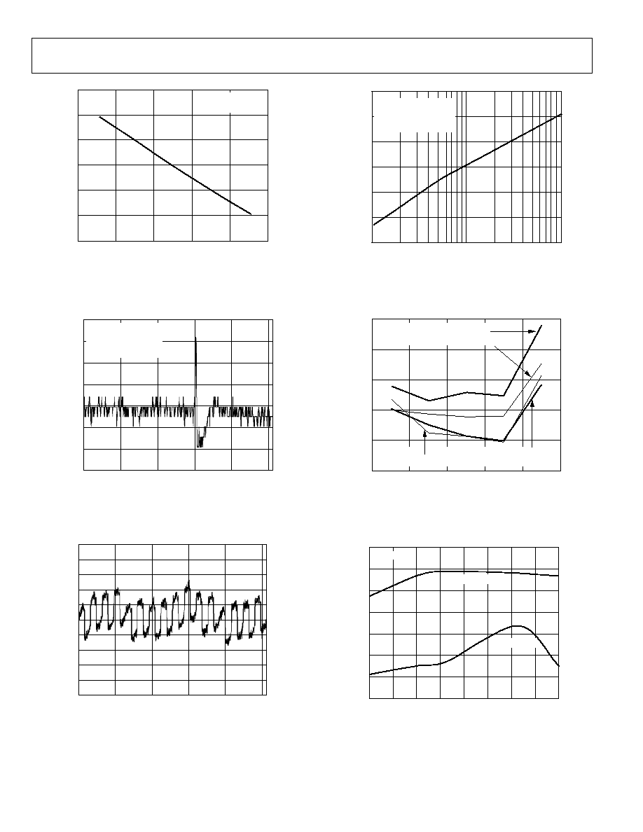
02883-A
-
021
2.00
2.7
3.1
3.5
3.9
4.3
4.7
5.1
2.9
3.3
3.7
4.1
4.5
4.9
5.3 5.5
V
CC
(V)
I
CC
(mA)
1.75
1.80
1.85
1.90
1.95
ADC OFF
DAC OUTPUTS AT 0V
Figure 22. Supply Current vs. Supply Voltage @ 25°C
02883-A
-
022
7
2.7 2.9 3.1 3.3 3.5 3.7 3.9 4.1 4.3 4.5 4.7 4.9 5.1 5.3 5.5
V
CC
(V)
I
CC
(mA)
0
1
2
3
4
5
6
Figure 23. Power-Down Current vs. Supply Voltage @ 25°C
4.0
0
2
4
6
8
1
TIME (
µ
s)
DAC OUTP
UT (V
)
0
0.5
1.0
1.5
2.0
2.5
3.0
3.5
0
02883-A
-
023
Figure 24. DAC Half-Scale Settling (1/4 to 3/4 Scale Code Change)
1.8
DAC OUTP
UT (V
)
0.8
1.0
1.2
1.4
1.6
0.6
0
2
4
TIME (
µ
s)
6
8
0.4
0.2
0
10
02883-A
-
024
Figure 25. Exiting Power-Down to Midscale
0.4700
0
2
4
6
8
10
TIME (
µ
s)
DAC OUTP
UT (V
)
0.4650
0.4655
0.4660
0.4665
0.4670
0.4675
0.4680
0.4685
0.4690
0.4695
02883-A
-
025
Figure 26. ADT7516 DAC Major Code Transition Glitch Energy;
011...11 to 100...00
0.4730
0
2
4
6
8
10
TIME (
µ
s)
DAC OUTP
UT (V
)
0.4685
0.4690
0.4695
0.4700
0.4705
0.4710
0.4715
0.4720
0.4725
02883-A
-
026
Figure 27. ADT7516 DAC Major Code Transition Glitch Energy;
100...00 to 011...11
ADT7516/ADT7517/ADT7519
Rev. A | Page 16 of 44
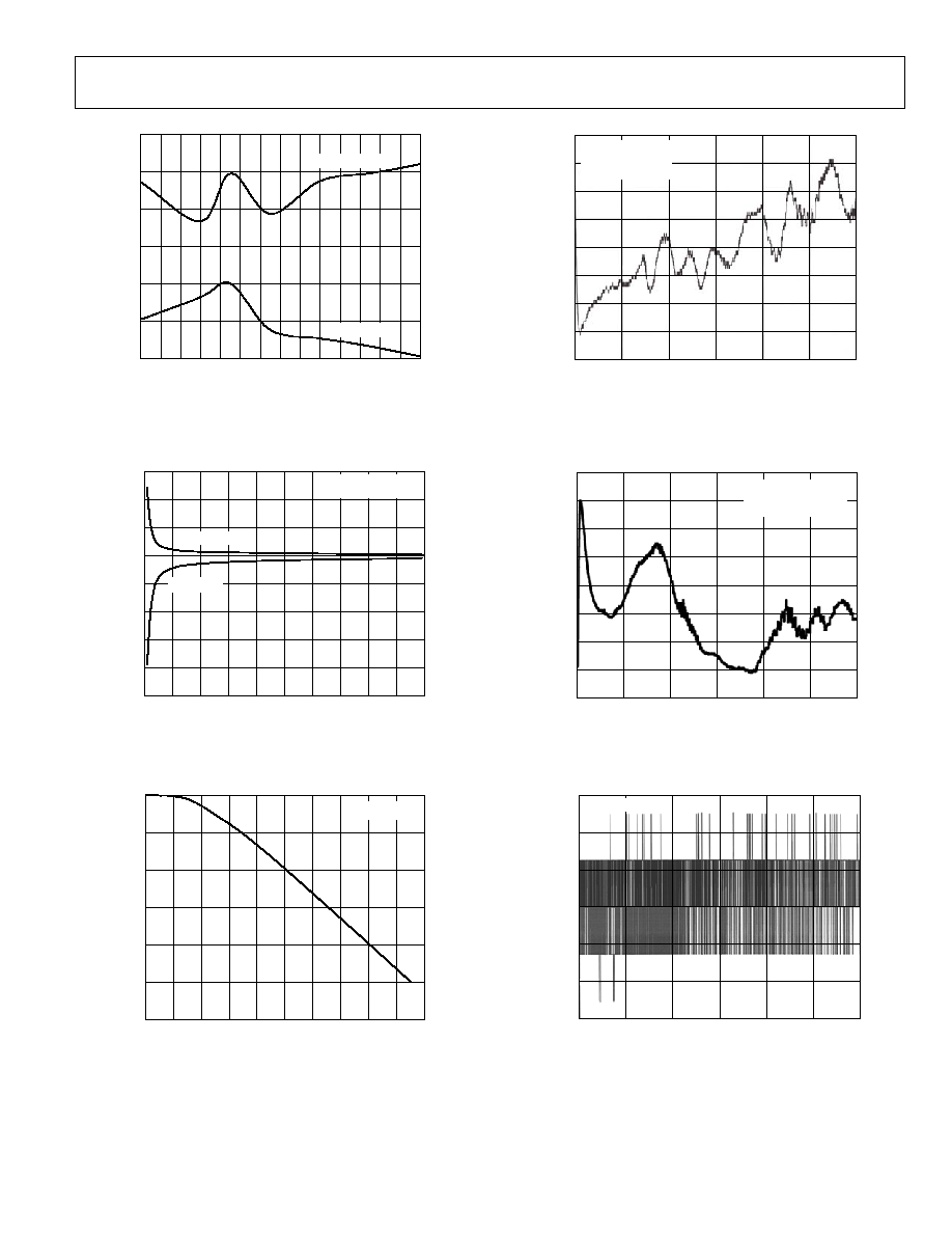
0
FULL-S
CALE
E
RROR (mV
)
12
10
8
6
4
2
1
2
3
V
REF
(V)
4
5
V
DD
= 5V
T
A
= 25
°
C
02
883-A
-
027
Figure 28. DAC Full-Scale Error vs. V
REF
2.329
0
1
2
3
4
TIME (
µ
s)
2.322
2.323
2.324
2.325
2.326
2.327
2.328
5
V
DD
= 5V
V
REF
= 5V
DAC OUTPUT LOADED
TO MIDSCALE
02883-A
-
028
DAC OUTP
UT (V
)
Figure 29. DAC-to-DAC Crosstalk
02883-A
-
029
1.0
0
200
400
600
800
1000
ADC CODE
INL E
RROR (LS
B
)
1.0
0.8
0.6
0.4
0.2
0
0.2
0.4
0.6
0.8
Figure 30. ADC INL with Ref = V
DD
(3.3 V)
02883-A
-
030
10
AC P
S
RR (dB)
60
50
40
30
20
0
1
10
100
FREQUENCY (kHz)
±100mV RIPPLE ON V
CC
V
REF
= 2.25V
V
DD
= 3.3V
TEMPERATURE = 25
°
C
Figure 31. PSRR vs. Supply Ripple Frequency
02883-A
-
031
TEMPERATURE (
°
C)
30
0
40
85
120
1.5
TE
MP
E
RATURE
E
RROR (
°
C)
1.0
0.5
0
0.5
1.0
EXTERNAL TEMPERATURE @ 3.3V
INTERNAL TEMPERATURE @ 5V
INTERNAL TEMPERATURE @ 3.3V
EXTERNAL TEMPERATURE @ 5V
Figure 32. Internal Temperature Error @ 3.3 V and 5 V
02883-A
-
032
E
RROR (LS
B
)
1
0
1
2
3
2
3
4
V
DD
= 3.3V
40
20
0
TEMPERATURE (
°
C)
20
40
60
80
100
120
GAIN ERROR
OFFSET ERROR
Figure 33. ADC Offset Error and Gain Error vs. Temperature
ADT7516/ADT7517/ADT7519
Rev. A | Page 17 of 44
02883-A
-
033
V
DD
(V)
E
RROR (LS
B
)
2.7
3.1
3.5
3.9
4.3
4.7
5.1
5.5
3
2
1
0
1
2
3
OFFSET ERROR
GAIN ERROR
Figure 34. ADC Offset Error and Gain Error vs. V
DD
02883-A
-
034
15
TE
MP
E
RATURE
E
RROR (
°
C)
10
5
0
5
10
15
20
25
0
10
20
PCB LEAKAGE RESISTANCE (M
)
30
40
50
60
70
80
90
100
V
DD
= 3.3V
TEMPERATURE = 25
°
C
D+ TO GND
D+ TO V
CC
Figure 35. External Temperature Error vs. PCB Leakage Resistance
02883-A
-
035
TE
MP
E
RATURE
E
RROR (
°
C)
60
50
40
30
20
10
0
V
DD
= 3.3V
0
5
10
15
20
25
CAPACITANCE (nF)
30
35
40
45
50
Figure 36. External Temperature Error vs. Capacitance between D+ and D
02883-A
-
036
10
TE
MP
E
RATURE
E
RROR (
°
C)
0
2
4
6
8
2
4
6
NOISE FREQUENCY (Hz)
V
DD
= 3.3V
COMMON-MODE
VOLTAGE = 100mV
1
100
200
300
400
500
600
Figure 37. External Temperature Error vs. Common-Mode Noise Frequency
02883-A
-
037
70
TE
MP
E
RATURE
E
RROR (
°
C)
20
30
40
50
60
10
0
10
1
100
200
NOISE FREQUENCY (MHz)
300
400
500
600
V
DD
= 3.3V
DIFFERENTIAL-MODE
VOLTAGE = 100mV
Figure 38. External Temperature Error vs. Differential-Mode Noise Frequency
02883-A
-
038
NOISE FREQUENCY (Hz)
±
250mV
V
DD
= 3.3V
1
100
200
300
400
500
600
0.6
TEMPERATURE ERROR (
°
C)
0.4
0.2
0
0.2
0.4
0.6
Figure 39. Internal Temperature Error vs. Power Supply Noise Frequency
ADT7516/ADT7517/ADT7519
Rev. A | Page 18 of 44
02883-A
-
039
140
TE
MP
E
RATURE
(
°
C)
40
60
80
100
120
20
0
10
20
TIME (s)
30
40
50
0
60
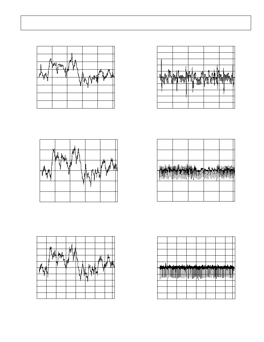
EXTERNAL TEMPERATURE
TEMPERATURE OF
ENVIRONMENT
CHANGED HERE
INTERNAL TEMPERATURE
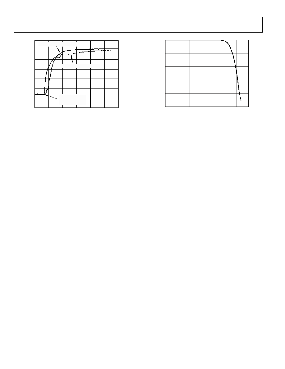
Figure 40. Temperature Sensor Response to Thermal Shock
0
ATTE
NUATION (dB)
25
20
15
10
5
1
10
100
1k
10k
100k
1M
10M
FREQUENCY (Hz)
02883-A
-
040
Figure 41. DAC Multiplying Bandwidth (Small Signal Frequency Response)

ADT7516/ADT7517/ADT7519
Rev. A | Page 19 of 44
THEORY OF OPERATION
Directly after the power-up calibration routine, the ADT7516/
ADT7517/ADT7519 go into idle mode. In this mode, the
devices are not performing any measurements and are fully
powered up. All four DAC outputs are at 0 V.
To begin monitoring, write to the Control Configuration 1
register (Address 18h) and set Bit C0 = 1. The ADT7516/
ADT7517/ADT7519 go into their power-up default measure-
ment mode, which is round robin. The devices proceed to take
measurements on the V
DD
channel, internal temperature sensor
channel, external temperature sensor channel, or AIN1 and
AIN2, AIN3, and finally AIN4. Once they finish taking
measurements on the AIN4 channel, the devices immediately
loop back to start taking measurements on the V
DD
channel and
repeats the same cycle as before. This loop continues until the
monitoring is stopped by resetting Bit C0 of the Control
Configuration 1 register to 0.
It is also possible to continue monitoring as well as switching to
single-channel mode by writing to the Control Configuration 2
register (Address 19h) and setting Bit C4 = 1. Further explana-
tion of the single-channel and round robin measurement modes
is given in later sections. All measurement channels have
averaging enabled on them on power-up. Averaging forces the
devices to take an average of 16 readings before giving a final
measured result. To disable averaging and consequently
decrease the conversion time by a factor of 16, set Bit C5 = 1 in
the Control Configuration 2 register.
There are four single-ended analog input channels on the
ADT7516/ADT7517/ADT7519: AIN1 to AIN4. AIN1 and AIN2
are multiplexed with the external temperature sensor terminals
D+ and D. Bits C1 and C2 of the Control Configuration 1
register (Address 18h) are used to select between AIN1/AIN2
and the external temperature sensor. The input range on the
analog input channels is dependent on whether the ADC
reference used is the internal V
REF
or V
DD
. To meet linearity
specifications, it is recommended that the maximum V
DD
value
is 5 V. Bit C4 of the Control Configuration 3 register is used to
select between the internal reference or V
DD
as the analog inputs'
ADC reference.
Controlling the DAC outputs can be done by writing to the
DACs' MSB and LSB registers (Addresses 10h to 17h). The
power-up default setting is to have a low going pulse on the
LDAC pin (Pin 9) controlling the updating of the DAC outputs
from the DAC registers. Alternatively, one can configure the
updating of the DAC outputs to be controlled by means other
than the LDAC pin by setting Bit C3 = 1 of the Control
Configuration 3 register (Address 1Ah). The DAC Configur-
ation register (Address 1Bh) and the LDAC Configuration
register (Address 1Ch) can now be used to control the DAC
updating. These two registers also control the output range of
the DACs and selecting between the internal or external refer-
ence. DAC A and DAC B outputs can be configured to give a
voltage output proportional to the temperature of the internal
and external temperature sensors, respectively.
The dual serial interface defaults to the I
2
C protocol on power-
up. To select and lock in the SPI protocol, follow the selection
process as described in the Serial Interface Selection section.
The I
2
C protocol cannot be locked in, while the SPI protocol
is automatically locked in on selection. The interface can be
switched back to be I
2
C on selection when the device is powered
off and on. When using I
2
C, the CS pin should be tied to either
V
DD
or GND.
There are a number of different operating modes on the
ADT7516/ADT7517/ADT7519 devices and all of them can be
controlled by the configuration registers. These features consist
of enabling and disabling interrupts, polarity of the INT/INT
pin, enabling and disabling the averaging on the measurement
channels SMBus timeout and software reset.
POWER-UP CALIBRATION
It is recommended that no communication to the part be ini-
tiated until approximately 5 ms after V
DD
has settled to within
10% of its final value. It is generally accepted that most systems
take a maximum of 50 ms to power up. Power-up time is
directly related to the amount of decoupling on the voltage
supply line.
During the 5 ms after V
DD
has settled, the part is performing a
calibration routine. Any communication to the device during
calibration will interrupt this routine, and could cause erro-
neous temperature measurements. If it is not possible to have
V
DD
at its nominal value by the time 50 ms has elapsed or if
communication to the device has started prior to V
DD
settling, it
is recommended that a measurement be taken on the V
DD
chan-
nel before a temperature measurement is taken. The V
DD
measurement is used to calibrate out any temperature measure-
ment error due to different supply voltage values.
CONVERSION SPEED
The internal oscillator circuit used by the ADC has the capa-
bility to output two different clock frequencies. This means that
the ADC is capable of running at two different speeds when
doing a conversion on a measurement channel. Thus, the time
taken to perform a conversion on a channel can be reduced by
setting Bit C0 of the Control Configuration 3 register (Address
1Ah). This increases the ADC clock speed from 1.4 kHz to
22 kHz. At the higher clock speed, the analog filters on the D+
and D input pins (external temperature sensor) are switched
off. This is why the power-up default setting is to have the ADC
working at the slow speed. The typical times for fast and slow
ADC speeds are given in the specifications.
ADT7516/ADT7517/ADT7519
Rev. A | Page 20 of 44
The ADT7516/ADT7517/ADT7519 power up with averaging
on. This means every channel is measured 16 times and
internally averaged to reduce noise. The conversion time can
also be sped up by turning off the averaging. This is done by
setting Bit C5 of the Control Configuration 2 register
(Address 19h) to 1.
FUNCTION DESCRIPTION--VOLTAGE OUTPUT
Digital-to-Analog Converters
The ADT7516/ADT7517/ADT7519 have four resistor string
DACs fabricated on a CMOS process with resolutions of 12, 10,
and 8 bits, respectively. They contain four output buffer ampli-
fiers and are written to via I
2
C serial interface or SPI serial inter-
face. See the Serial Interface section for more information.
The ADT7516/ADT7517/ADT7519 operate from a single sup-
ply of 2.7 V to 5.5 V, and the output buffer amplifiers provide
rail-to-rail output swing with a slew rate of 0.7 V/µs. All four
DACs share a common reference input, V
REF
-IN. The reference
input is buffered to draw virtually no current from the reference
source because it offers the source a high impedance input. The
devices have a power-down mode in which all DACs may be
turned off completely with a high impedance output.
Each DAC output will not be updated until it receives the
LDAC command. Therefore, while the DAC registers would
have been written to with a new value, this value will not be
represented by a voltage output until the DACs have received
the LDAC command. Reading back from any DAC register
prior to issuing an LDAC command will result in the digital
value that corresponds to the DAC output voltage. Thus, the
digital value written to the DAC register cannot be read back
until after the LDAC command has been initiated. This LDAC
command can be given by either pulling the LDAC pin low
(falling edge loads DACs), setting up Bits D4 and D5 of the
DAC configuration register (Address 1Bh), or using the LDAC
register (Address 1Ch).
When using the LDAC pin to control the DAC register loading,
the low going pulse width should be 20 ns minimum. The
LDAC pin has to go high and low again before the DAC
registers can be reloaded.
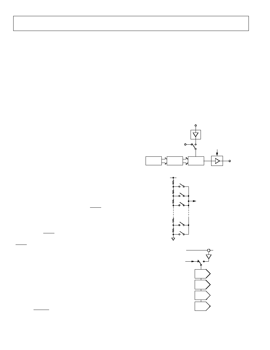
Digital-to-Analog Section
The architecture of one DAC channel consists of a resistor
string DAC followed by an output buffer amplifier. The voltage
at the V
REF
-IN pin or the on-chip reference of 2.28 V provides
the reference voltage for the corresponding DAC. Figure 42
shows a block diagram of the DAC architecture. Since the input
coding to the DAC is straight binary, the ideal output voltage is
given by
N
REF
OUT
D
V
V
2
×
=
where:
D = decimal equivalent of the binary code that is loaded to the
DAC register:
0 to 255 for ADT7519 (8 bits)
0 to 1023 for ADT7517 (10 bits)
0 to 4095 for ADT7516 (12 bits)
N = DAC resolution
Resistor String
The resistor string section is shown in Figure 43. It is simply a
string of resistors, each of approximately 603 . The digital
code loaded to the DAC register determines at which node on
the string the voltage is tapped off to be fed into the output
amplifier. The voltage is tapped off by closing one of the
switches connecting the string to the amplifier. Because it is a
string of resistors, it is guaranteed monotonic.
INPUT
REGISTER
DAC
REGISTER
RESISTOR
STRING
V
OUT
-A
OUTPUT BUFFER
AMPLIFIER
GAIN MODE
(GAIN = 1 OR 2)
REFERENCE
BUFFER
INT V
REF
V
REF
-IN
02883-A
-
041
Figure 42. Single DAC Channel Architecture
R
R
R
R
R
TO OUTPUT
AMPLIFIER
02883-A
-
042
Figure 43. Resistor String
STRING
DAC A
2.28V
INTERNAL V
REF
V
REF
-IN
STRING
DAC B
STRING
DAC C
STRING
DAC D
02883-A
-
043
Figure 44. DAC Reference Buffer Circuit
ADT7516/ADT7517/ADT7519
Rev. A | Page 21 of 44
DAC Reference Inputs
There is an input reference pin for the DACs. This reference
input is buffered (see Figure 44).
The advantage with the buffered input is the high impedance it
presents to the voltage source driving it. The user can have an
external reference voltage as low as 1 V and as high as V
DD
. The
restriction of 1 V is due to the footroom of the reference buffer.
The LDAC configuration register controls the option to select
between internal and external voltage references. The default
setting is for external reference selected.
Output Amplifier
The output buffer amplifier can generate output voltages to
within 1 mV of either rail. Its actual range depends on the value
of V
REF
, gain, and offset error.
If a gain of 1 is selected (Bits 0 to 3 of the DAC configuration
register = 0), the output range is 0.001 V to V
REF
.
If a gain of 2 is selected (Bits 0 to 3 of the DAC configuration
register = 1), the output range is 0.001 V to 2 V
REF
. Because
of clamping, however, the maximum output is limited to
V
DD
0.001 V.
The output amplifier can drive a load of 4.7 k to GND or V
DD
,
in parallel with 200 pF to GND or V
DD
(see Figure 5). The
source and sink capabilities of the output amplifier can be seen
in the plot of Figure 20.
The slew rate is 0.7 V/µs with a half-scale settling time to
±0.5 LSB (at 8 bits) of 6 µs.
Thermal Voltage Output
The ADT7516/ADT7517/ADT7519 can output voltages that are
proportional to temperature. DAC A output can be configured
to represent the temperature of the internal sensor while DAC B
output can be configured to represent the external temperature
sensor. Bits C5 and C6 of the Control Configuration 3 register
select the temperature proportional output voltage. Each time a
temperature measurement is taken, the DAC output is updated.
The output resolution for the ADT7519 is 8 bits with 1°C
change corresponding to 1 LSB change. The output resolution
for the ADT7516 and ADT7517 are capable of 10 bits with
0.25°C change corresponding to 1 LSB change. The default
output resolution for the ADT7516 and ADT7517 is 8 bits. To
increase this to 10 bits, set C1 = 1 in the Control Configuration
3 register. The default output range is 0 V to V
REF
and this can be
increased to 0 V to 2 V
REF
. Increasing the output voltage span to
2 V
REF
can be done by setting D0 = 1 for DAC A (internal temp-
erature sensor) and D1 = 1 for DAC B (external temperature
sensor) in the DAC configuration register (Address 1Bh).
The output voltage is capable of tracking a maximum temp-
erature range of 128°C to +127°C, but the default setting is
40°C to +127°C. If the output voltage range is 0 V to V
REF
-IN
(V
REF
-IN = 2.25 V), then this corresponds to 0 V representing
40°C, and 1.48 V representing +127°C. This, of course, will
give an upper deadband between 1.48 V and V
REF
.
The internal and external analog temperature offset registers
can be used to vary this upper deadband and, consequently, the
temperature that 0 V corresponds to. Table 6 and Table 7 give
examples of how this is done using a DAC output voltage span
of V
REF
and 2 V
REF
, respectively. Simply write in the temperature
value, in twos complement format, at which 0 V is to start. For
example, if using the DAC A output and 0 V to start at 40°C,
program D8h into the internal analog temperature offset reg-
ister (Address 21h). This is an 8-bit register and has a temp-
erature offset resolution of only 1°C for all device models. Use
the formulas following the tables to determine the value to
program into the offset registers.
Table 6. Thermal Voltage Output (0 V to V
REF
)
O/P Voltage (V)
Default °C
Max °C
Sample °C
0
40
128
0
0.5
+17
71
+56
1
+73
15
+113
1.12
+87
1
+127
1.47
+127
+39
UDB
1.5
UDB
+42
UDB
2
UDB
+99
UDB
2.25
UDB
+127
UDB
Upper deadband has been reached. DAC output is not capable of
increasing. See Fig
.
ure 9
C1
D+
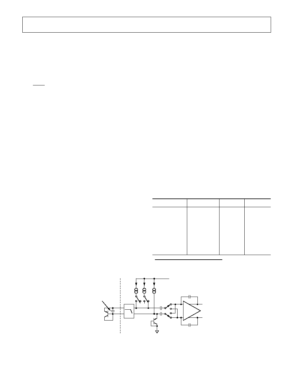
LOW-PASS
FILTER
f
C
= 65kHz
BIAS
DIODE
V
DD
TO ADC
V
OUT+
V
OUT
REMOTE
SENSING
TRANSISTOR
(2N3906)
OPTIONAL CAPACITOR, UP TO
3nF MAX. CAN BE ADDED TO
IMPROVE HIGH FREQUENCY
NOISE REJECTION IN NOISY
ENVIRONMENTS
D
I
N
×
I
I
BIAS
02883-A
-
044
Figure 45. Signal Conditioning for External Diode Temperature Sensor
ADT7516/ADT7517/ADT7519
Rev. A | Page 22 of 44
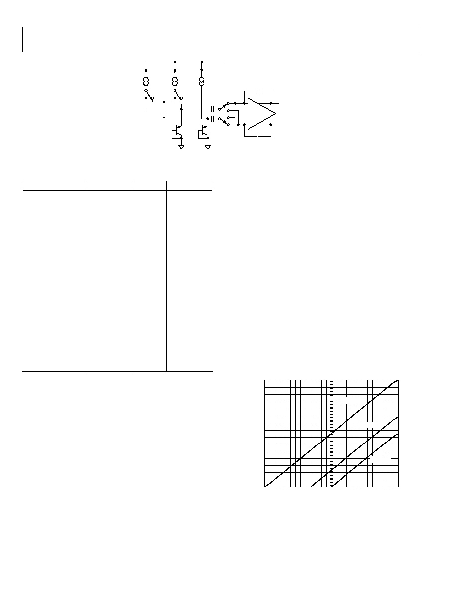
BIAS
DIODE
INTERNAL
SENSE
TRANSISTOR
V
DD
TO ADC
V
OUT+
V
OUT
I
N
×
I
I
BIAS
02883-A
-
045
Figure 46. Top Level Structure of Internal Temperature Sensor
Table 7. Thermal Voltage Output (0 V to 2V
REF
)
O/P Voltage (V)
Default °C
Max °C
Sample °C
0
40
128
0
0.25
26
114
+14
0.5
+12
100
+28
0.75
+3
85
+43
1
+17
71
+57
1.12
+23
65
+63
1.47
+43
45
+83
1.5
+45
43
+85
2
+73
15
+113
2.25
+88
0
+127
2.5
+102
+14
UDB
2.75
+116
+28
UDB
3
UDB
+42
UDB
3.25
UDB
+56
UDB
3.5
UDB
+70
UDB
3.75
UDB
+85
UDB
4
UDB
+99
UDB
4.25
UDB
+113
UDB
4.5
UDB
+127
UDB
Negative temperatures:
( )
(
)
128
0
+
=
Temp
V
d
Code
Register
Offset
where:
D7 of Offset Register Code is set to 1 for negative temperatures.
Example:
( )
(
)
58h
d
d
Code
Register
Offset
=
=
+
-
=
88
128
40
Since a negative temperature has been inserted into the
equation, DB7 (MSB) of the offset register code is set to 1.
Therefore 58h becomes D8h.
58h + DB7(1) = D8h
Positive temperatures:
Offset Register Code (d) = 0 V Temp
Example:
Offset Register Code (d) = 10d = 0Ah
The following equation is used to work out the various
temperatures for the corresponding 8-bit DAC output:
(
) (
)
Temp
V
LSB
P
O
DAC
Temp
Bit
0
1
/
8
+
÷
=
-
For example, if the output is 1.5 V, V
REF
-IN
= 2.25 V, 8-bit DAC
has an LSB size = 2.25 V/256 = 8.79 × 10
3
, and 0 V temp is at
128°C, then the resultant temperature is
(
)
(
)
C
°
+
=
-
+
×
÷
-
43
128
10
79
.
8
5
.
1
3
The following equation is used to work out the various
temperatures for the corresponding 10-bit DAC output:
10-Bit Temp = ((DAC O/P ÷ 1 LSB) × 0.25) + (0 V Temp)
For example, if the output is 0.4991 V, V
REF
-IN = 2.25 V, 10-bit
DAC has an LSB size = 2.25 V/1024 = 2.197 × 10
3
, and 0 V
temp is at 40°C, then the resulting temperature is
(((0.4991 ÷ 2.197 × 10
3
) × 0.25) + (40) = +16.75°C
Figure 47 shows a graph of the DAC output versus temperature
for a V
REF
-IN = 2.25 V.
TEMPERATURE (
°
C)
DAC OUTP
UT (V
)
0
0.15
128110 90 70 50 30 10 10
30
50
70
90 110 127
0.30
0.45
0.60
0.75
0.90
1.05
1.20
1.35
1.50
1.65
1.80
1.95
2.10
2.25
0V = 128
°
C
0V = 40
°
C
0V = 0
°
C
02883-A
-
046
Figure 47. DAC Output vs. Temperature V
REF
-IN = 2.25 V
ADT7516/ADT7517/ADT7519
Rev. A | Page 23 of 44
FUNCTIONAL DESCRIPTION--ANALOG INPUTS
Single-Ended Inputs
The ADT7516/ADT7517/ADT7519 offer four single-ended
analog input channels. The analog input range is from 0 V to
2.28 V, or 0 V to V
DD
. To maintain the linearity specification, it is
recommended that the maximum V
DD
value be set at 5 V.
Selection between the two input ranges is done by Bit C4 of the
Control Configuration 3 register (Address 1Ah). Setting this bit
to 0 sets up the analog input ADC reference to be sourced from
the internal voltage reference of 2.28 V. Setting the bit to 1 sets
up the ADC reference to be sourced from V
DD
.
The ADC resolution is 10 bits and is mostly suitable for dc input
signals. Bits C1:2 of the Control Configuration 1 register
(Address 18h) are used to set up Pins 7 and 8 as AIN1 and
AIN2. Figure 48 shows the overall view of the 4-channel analog
input path.
M
U
L
T
I
P
L
E
X
E
R
10-BIT
ADC
TO ADC
VALUE
REGISTER
AIN1
AIN2
AIN3
AIN4
02883-A
-
047
Figure 48. Quad Analog Input Path
Converter Operation
The analog input channels use a successive approximation ADC
based on a capacitor DAC. Figure 49 and Figure 50 show sim-
plified schematics of the ADC. Figure 49 shows the ADC during
acquisition phase. SW2 is closed and SW1 is in Position A. The
comparator is held in a balanced condition and the sampling
capacitor acquires the signal on AIN.
CONTROL
LOGIC
CAP DAC
ACQUISITION
PHASE
SAMPLING
CAPACITOR
COMPARATOR
INT V
REF
REF
V
DD
AIN
SW1
A
B
SW2
REF/2
02883-A
-
048
Figure 49. ADC Acquisition Phase
CONTROL
LOGIC
CAP DAC
CONVERSION
PHASE
SAMPLING
CAPACITOR
COMPARATOR
INT V
REF
REF
V
DD
AIN
SW1
A
B
SW2
REF/2
02883-A
-
049
Figure 50. ADC Conversion Phase
When the ADC eventually goes into conversion phase (see
Figure 50), SW2 opens and SW1 moves to position B, causing
the comparator to become unbalanced. The control logic and
the DAC are used to add and subtract fixed amounts of charge
from the sampling capacitor to bring the comparator back into
a balanced condition. When the comparator is rebalanced, the
conversion is complete. The control logic generates the ADC
output code. Figure 51 shows the ADC transfer function for the
analog inputs.
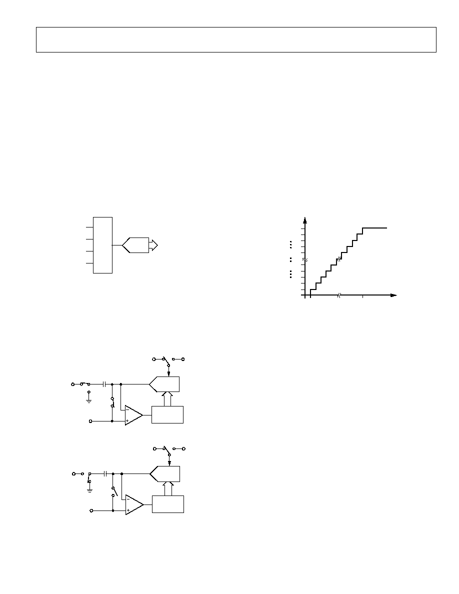
ADC TRANSFER FUNCTION
The output coding of the ADT7516/ADT7517/ADT7519 analog
inputs is straight binary. The designed code transitions occur
midway between successive integer LSB values (i.e., 1/2 LSB,
3/2 LSB). The LSB is V
DD
/1024 or internal V
REF
/1024, internal
V
REF
= 2.28 V. The ideal transfer characteristic is shown in
Figure 51.
111...111
111...110
111...000
011...111
+V
REF
1LSB
0V 1/2LSB
ANALOG INPUT
ADC CODE
1LSB = INT V
REF
/1024
1LSB = V
DD
/1024
000...010
000...001
000...000
02883-A
-
050
Figure 51. Single-Ended Transfer Function
To work out the voltage on any analog input channel, the
following method can be used:
1 LSB = reference (v)/1024
Convert value read back from AIN value register into decimal.
( )
size
LSB
d
value
AIN
voltage
AIN
×
=
d = decimal
Example:
Internal reference used. Therefore V
REF
= 2.28 V.
AIN value = 512d
3
10
226
.
2
1024
/
28
.
2
1
-
×
=
=
V
size
LSB
V
voltage
AIN
14
.
1
10
226
.
2
512
3
=
×
×
=
-
ADT7516/ADT7517/ADT7519
Rev. A | Page 24 of 44
Analog Input ESD Protection
Figure 52 shows the input structure on any of the analog input
pins that provides ESD protection. The diode provides the main
ESD protection for the analog inputs. Care must be taken that
the analog input signal never drops below the GND rail by
more than 200 mV. If this happens, the diode will become
forward-biased and start conducting current into the substrate.
The 4 pF capacitor is the typical pin capacitance and the resistor
is a lumped component made up of the on resistance of the
multiplexer switch.
4pF
AIN
100
02883-A
-
051
Figure 52. Equivalent Analog Input ESD Circuit
AIN Interrupts
The measured results from the AIN inputs are compared with
the AIN V
HIGH
(greater than comparison) and V
LOW
(less than or
equal to comparison) limits. An interrupt occurs if the AIN
inputs exceed or equal the limit registers. These voltage limits
are stored in on-chip registers. Note that the limit registers are 8
bits long while the AIN conversion result is 10 bits long. If the
voltage limits are not masked out, then any out-of-limit com-
parisons generate flags that are stored in the Interrupt Status 1
register (Address = 00h) and one or more out-of-limit results
will cause the INT/INT output to pull either high or low
depending on the output polarity setting. It is good design
practice to mask out interrupts for channels that are of no
concern to the application. Figure 53 shows the interrupt
structure for the ADT7516/ ADT7517/ADT7519. It gives a
block diagram representation of how the various measurement
channels affect the INT/INT pin.
Upper deadband has been reached. DAC output is not capable of increasing.
See
.
Figure 9
WATCHDOG
LIMIT
COMPARISONS
INTERRUPT
MASK
REGISTERS
CONTROL
CONFIGURATION
REGISTER 1
INTERRUPT
STATUS
REGISTER
(TEMP AND
AIN1 TO AIN4)
INTERRUPT
STATUS
REGISTER 2
(V
DD
)
S
T
ATUS
BITS
S
T
ATUS
BIT
READ RESET
S/W RESET
INTERNAL
TEMP
INT/INT
(LATCHED OUTPUT)
INT/INT
ENABLE BIT
EXTERNAL
TEMP
V
DD
DIODE
FAULT
AIN1AIN4
02883-A
-
052
Figure 53. ADT7516/ADT7517/ADT7519 Interrupt Structure

ADT7516/ADT7517/ADT7519
Rev. A | Page 25 of 44
FUNCTIONAL DESCRIPTION--MEASUREMENT
Temperature Sensor
The ADT7516/ADT7517/ADT7519 contain an ADC with
special input signal conditioning to enable operation with
external and on-chip diode temperature sensors. When the
ADT7516/ADT7517/ADT7519 is operating in single-channel
mode, the ADC continually processes the measurement taken
on one channel only. This channel is preselected by Bits C0:C2
in the Control Configuration 2 register (Address 19h). When in
round robin mode, the analog input multiplexer sequentially
selects the V
DD
input channel, the on-chip temperature sensor to
measure its internal temperature, either the external temper-
ature sensor or AIN1 and AIN2, AIN3, and then AIN4. These
signals are digitized by the ADC and the results are stored in the
various value registers.
The measured results from the temperature sensors are com-
pared with the internal and external T
HIGH
, T
LOW
limits. These
temperature limits are stored in on-chip registers. If the temp-
erature limits are not masked, any out-of-limit comparisons
generate flags that are stored in the Interrupt Status 1 register.
One or more out-of-limit results will cause the INT/INT output
to pull either high or low depending on the output polarity
setting.
Theoretically, the temperature measuring circuit can measure
temperatures from 128°C to +127°C with a resolution of
0.25°C. However, temperatures outside T
A
are outside the
guaranteed operating temperature range of the device. Temp-
erature measurement from 128°C to +127°C is possible using
an external sensor.
Temperature measurement is initiated by three methods. The
first method is applicable when the part is in single-channel
measurement mode. The temperature is measured 16 times and
internally averaged to reduce noise. In single-channel mode, the
part is continuously monitoring the selected channel, i.e., as
soon as one measurement is taken another one is started on the
same channel. The total time to measure a temperature channel
with the ADC operating at slow speed is typically 11.4 ms
(712 µs × 16) for the internal temperature sensor and 24.22 ms
(1.51 ms × 16) for the external temperature sensor. The new
temperature value is stored in two 8-bit registers and is ready
for reading by the I
2
C or SPI interface. The user has the option
of disabling the averaging by setting Bit 5 in the Control
Configuration 2 register (Address 19h). The ADT7516/
ADT7517/ADT7519 default on power-up with averaging
enabled.
The second method is applicable when the part is in round
robin measurement mode. The part measures both the internal
and external temperature sensors as it cycles through all pos-
sible measurement channels. The two temperature channels are
measured each time the part runs a round robin sequence. In
round robin mode, the part is continuously measuring all
channels.
Temperature measurement is also initiated after every read or
write to the part when the part is in either single-channel
measurement mode or round robin measurement mode.
Once serial communication has started, any conversion in pro-
gress stops and the ADC resets. Conversion restarts immedi-
ately after the serial communication has finished. The temp-
erature measurement proceeds normally as described above.
V
DD
Monitoring
The ADT7516/ADT7517/ADT7519 also have the ability to
monitor its own power supply. The part measures the voltage on
its V
DD
pin to a resolution of 10 bits. The resulting value is
stored in two 8-bit registers; the two LSBs are stored in register
address 03h and the eight MSBs are stored in register address
06h. This allows the option of doing just a 1-byte read if 10-bit
resolution is not important. The measured result is compared
with the V
HIGH
and V
LOW
limits. If the V
DD
interrupt is not
masked, any out-of-limit comparison generates a flag in the
Interrupt Status 2 register and one or more out-of-limit results
will cause the INT/INT output to pull either high or low,
depending on the output polarity setting.
Measuring the voltage on the V
DD
pin is regarded as monitoring
a channel along with the internal, external, and AIN channels.
The user can select the V
DD
channel for single-channel
measurement by setting Bit C4 = 1 and setting Bits C0:C2 to all
0s in the Control Configuration 2 register.
When measuring the V
DD
value, the reference for the ADC is
sourced from the internal reference. Table 8 shows the data
format. As the maximum V
DD
voltage measurable is 7 V, internal
scaling is performed on the V
DD
voltage to match the 2.28 V
internal reference value. Below is an example of how the
transfer function works.
V
DD
= 5 V
ADC Reference = 2.28 V
1
LSB = ADC Reference/2
10
=
2.28/1024
=
2.226
mV
Scale Factor = Full-scale V
CC
/ADC Reference
=
7/2.28
=
3.07
Conversion Result = V
DD
/(Scale Factor × LSB size)
= 5/(3.07 × 2.226 mV)
= 2 DCh

ADT7516/ADT7517/ADT7519
Rev. A | Page 26 of 44
Table 8. V
DD
Data Format (V
REF
= 2.28 V)
Digital Output
V
DD
Value (V)
Binary
Hex
2.7
01 1000 1011
18B
3
01 1011 0111
1B7
3.5
10 0000 0000
200
4
10 0100 1001
249
4.5
10 1001 0010
292
5
10 1101 1100
2DC
5.5
11 0010 0101
325
6
11 0110 1110
36E
6.5
11 1011 0111
3B7
7
11 1111 1111
3FF
On-Chip Reference
The ADT7516/ADT7517/ADT7519 have an on-chip 1.2 V band
gap reference, which is gained up by a switched capacitor ampli-
fier to give an output of 2.28 V. The amplifier is powered up for
the duration of the device monitoring phase and is powered
down once monitoring is disabled. This saves on current con-
sumption. The internal reference is used as the reference for the
ADC. The ADC is used for measuring V
DD
, internal temperature
sensor, external temperature sensor, and AIN inputs. The
internal reference is always used when measuring V
DD
, and the
internal and external temperature sensors. The external
reference is the default power-up reference for the DACs.
Round Robin Measurement
On power-up, the ADT7516/ADT7517/ADT7519 go into round
robin mode but monitoring is disabled. Setting Bit C0 of the
Configuration Register 1 to 1 enables conversions. It sequences
through all the available channels, taking a measurement from
each in the following order: V
DD
, internal temperature sensor,
external temperature sensor/(AIN1 and AIN2), AIN3, and
AIN4. Pin 7 and Pin 8 can be configured to be either external
temperature sensor pins or standalone analog input pins. Once
conversion is completed on the AIN4 channel, the device loops
around for another measurement cycle. This method of taking a
measurement on all the channels in one cycle is called round
robin. Setting Bit C4 of Control Configuration 2 (Address 19h)
disables the round robin mode and in turn sets up the single-
channel mode. The single-channel mode is where only one
channel, e.g., internal temperature sensor, is measured in each
conversion cycle.
The time taken to monitor all channels will normally not be of
interest, since the most recently measured value can be read at
any time. For applications where the round robin time is impor-
tant, typical times at 25°C are given in the specifications.
Single-Channel Measurement
Setting C4 of the Control Configuration 2 register enables the
single-channel mode and allows the ADT7516/ADT7517/
ADT7519 to focus on one channel only. A channel is selected by
writing to Bits C0:C2 in the Control Configuration 2 register.
For example, to select the V
DD
channel for monitoring, write to
the Control Configuration 2 register and set C4 to 1 (if not
done so already), then write all 0s to Bits C0:C2. All subsequent
conversions will be done on the V
DD
channel only. To change the
channel selection to the internal temperature channel, write to
the Control Configuration 2 register and set C0 = 1. When
measuring in single-channel mode, conversions on the channel
selected occur directly after each other. Any communication to
the ADT7516/ADT7517/ADT7519 stops the conversions, but
they are restarted once the read or write operation is completed.
Temperature Measurement Method
Internal Temperature Measurement
The ADT7516/ADT7517/ADT7519 contain an on-chip band
gap temperature sensor whose output is digitized by the on-chip
ADC. The temperature data is stored in the Internal Temper-
ature Value register. Because both positive and negative temper-
atures can be measured, the temperature data is stored in twos
complement format, as shown in Table 9. The thermal charac-
teristics of the measurement sensor could change and, therefore,
an offset is added to the measured value to enable the transfer
function to match the thermal characteristics. This offset is
added before the temperature data is stored. The offset value
used is stored in the internal temperature offset register.
External Temperature Measurement
The ADT7516/ADT7517/ADT7519 can measure the temper-
ature of one external diode sensor or diode-connected
transistor.
The forward voltage of a diode or diode-connected transistor,
operated at a constant current, exhibits a negative temperature
coefficient of about 2 mV/°C. Unfortunately, because the
absolute value of V
BE
varies from device to device, and indivi-
dual calibration is required to null this out, the technique is
unsuitable for mass production.
The technique used in the ADT7516/ADT7517/ADT7519 is to
measure the change in V
BE
when the device is operated at two
different currents. This is given by
( )
N
n
q
KT
V
BE
1
/ ×
=
where:
K is Boltzmann's constant.
q is the charge on the carrier.
T is the absolute temperature in kelvins.
N is the ratio of the two currents.
Figure 45 shows the input signal conditioning used to measure
the output of an external temperature sensor. This figure shows
the external sensor as a substrate transistor, provided for temp-
erature monitoring on some microprocessors, but it could
equally well be a discrete transistor.

ADT7516/ADT7517/ADT7519
Rev. A | Page 27 of 44
If a discrete transistor is used, the collector will not be
grounded, and should be linked to the base. If a PNP transistor
is used, the base is connected to the D input and the emitter to
the D+ input. If an NPN transistor is used, the emitter is
connected to the D input and the base to the D+ input.
A 2N3906 is recommended as the external transistor.
To prevent ground noise interfering with the measurement, the
more negative terminal of the sensor is not referenced to
ground, but is biased above ground by an internal diode at the
D input. As the sensor is operating in a noisy environment, C1
is provided as a noise filter. See the Layout Considerations
section for more information on C1.
To measure V
BE
, the sensor is switched between operating
currents of I and N × I. The resulting waveform is passed
through a low-pass filter to remove noise, then to a chopper-
stabilized amplifier that performs the functions of amplification
and rectification of the waveform to produce a dc voltage
proportional to V
BE
. This voltage is measured by the ADC to
give a temperature output in 10-bit twos complement format. To
further reduce the effects of noise, digital filtering is performed
by averaging the results of 16 measurement cycles.
Layout Considerations
Digital boards can be electrically noisy environments, and care
must be taken to protect the analog inputs from noise, particu-
larly when measuring the very small voltages from a remote
diode sensor. The following precautions should be taken:
1.
Place the ADT7516/ADT7517/ADT7519 as close as
possible to the remote sensing diode. Provided that the
worst noise sources such as clock generators, data/address
buses, and CRTs are avoided, this distance can be 4 inches
to 8 inches.
2.
Route the D+ and D tracks close together, in parallel, with
grounded guard tracks on each side. Provide a ground
plane under the tracks, if possible.
3.
Use wide tracks to minimize inductance and reduce noise
pickup. A 10 mil track minimum width and spacing is
recommended.
GND
D+
D
GND
10 MIL
10 MIL
10 MIL
10 MIL
10 MIL
10 MIL
10 MIL
02883-A
-
053
Figure 54. Arrangement of Signal Tracks
4.
Try to minimize the number of copper/solder joints, which
can cause thermocouple effects. Where copper/solder
joints are used, make sure that they are in both the D+ and
D path and at the same temperature.
Thermocouple effects should not be a major problem
because 1°C corresponds to about 240 µV, and
thermocouple voltages are about 3 µV/°C of temperature
difference. Unless there are two thermocouples with a big
temperature differential between them, thermocouple
voltages should be much less than 200 mV.
5.
Place 0.1 µF bypass and 2200 pF input filter capacitors
close to the ADT7516/ADT7517/ADT7519.
6.
If the distance to the remote sensor is more than 8 inches,
the use of twisted-pair cable is recommended. This will
work up to about 6 feet to 12 feet.
7.
For long distances (up to 100 feet), use shielded twisted-
pair cable, such as Belden #8451 microphone cable. Con-
nect the twisted pair to D+ and D. and the shield to GND
close to the ADT7516/ADT7517/ADT7519. Leave the
remote end of the shield unconnected to avoid ground
loops.
Because the measurement technique uses switched current
sources, excessive cable and/or filter capacitance can affect the
measurement. When using long cables, the filter capacitor may
be reduced or removed.
Cable resistance can also introduce errors. Series resistance of
1 introduces about 0.5°C error.
Temperature Value Format
One LSB of the ADC corresponds to 0.25°C. The ADC can
theoretically measure a temperature span of 255°C. The internal
temperature sensor is guaranteed to a low value limit of 40°C.
It is possible to measure the full temperature span using the
external temperature sensor. The temperature data format is
shown in Table 9.
The result of the internal or external temperature measure-
ments is stored in the temperature value registers, and is com-
pared with limits programmed into the internal or external high
and low registers.
ADT7516/ADT7517/ADT7519
Rev. A | Page 28 of 44
Table 9. Temperature Data Format (Internal and External
Temperature)
Temperature
Digital Output
40°C
11 0110 0000
25°C
11 1001 1100
10°C
11 1101 1000
0.25°C
11 1111 1111
0°C
00 0000 0000
+0.25°C
00 0000 0001
+10°C
00 0010 1000
+25°C
00 0110 0100
+50°C
00 1100 1000
+75°C
01 0010 1100
+100°C
01 1001 0000
+105°C
01 1010 0100
+125°C
01 1111 0100
Temperature conversion formula:
Positive Temperature = ADC Code/4
Negative Temperature = (ADC Code* 512)/4
*where DB9 is removed from the ADC code.
Interrupts
The measured results from the internal temperature sensor,
external temperature sensor, V
DD
pin, and AIN inputs are
compared with the T
HIGH
/V
HIGH
(greater than comparison) and
T
LOW
/V
LOW
(less than or equal to comparison) limits. An inter-
rupt occurs if the measurement exceeds or equals the limit
registers. These limits are stored in on-chip registers. Note that
the limit registers are 8 bits long while the conversion results are
10 bits long. If the limits are not masked, any out-of-limit com-
parisons generate flags that are stored in the Interrupt Status 1
register (Address 00h) and Interrupt Status 2 register
(Address 01h). One or more out-of-limit results will cause the
INT/INT output to pull either high or low depending on the
output polarity setting. It is good design practice to mask out
interrupts for channels that are of no concern to the application.
Figure 53 shows the interrupt structure for the ADT7516/
ADT7517/ADT7519. It gives a block diagram representation of
how the various measurement channels affect the INT/INT pin.
ADT7516/ADT7517/ADT7519 REGISTERS
The ADT7516/ADT7517/ADT7519 contain registers that are
used to store the results of external and internal temperature
measurements, V
DD
value measurements, analog input measure-
ments, high and low temperature limits, supply voltage and
analog input limits, set output DAC voltage levels, configure
multipurpose pins, and generally to control the device. A
description of these registers follows.
The register map is divided into registers of 8 bits. Each register
has its own individual address, but some consist of data that is
linked with other registers. These registers hold the 10-bit
conversion results of measurements taken on the temperature,
V
DD
, and AIN channels. For example, the eight MSBs of the V
DD
measurement are stored in register Address 06h while the two
LSBs are stored in register Address 03h. The link involved
between these types of registers is that when the LSB register is
read first, the MSB registers associated with that LSB register are
locked to prevent any updates. To unlock these MSB registers,
the user has only to read any one of them, which will have the
effect of unlocking all previously locked MSB registers. So for
the preceding example, if Register 03h was read first, MSB
Registers 06h and 07h would be locked to prevent any updates
to them. If Register 06h was read, this register and Register 07h
would be subsequently unlocked.
LOCK ASSOCIATED
MSB REGISTERS
FIRST READ
COMMAND
LSB
REGISTER
OUTPUT
DATA
02883-A
-
054
Figure 55. Phase 1 of 10-Bit Read
UNLOCK ASSOCIATED
MSB REGISTERS
SECOND READ
COMMAND
MSB
REGISTER
OUTPUT
DATA
02883-A
-
055
Figure 56. Phase 2 of 10-Bit Read
If an MSB register is read first, its corresponding LSB register is
not locked, leaving the user with the option of just reading back
8 bits (MSB) of a 10-bit conversion result. Reading an MSB
register first does not lock other MSB registers, and likewise
reading an LSB register first does not lock other LSB registers.
Table 10. ADT7516/ADT7517/ADT7519 Registers
RD/WR
Address
Name
Power-On
Default
00h
Interrupt Status 1
00h
01h
Interrupt Status 2
00h
02h
Reserved
03h
Internal Temp and V
DD
LSBs
00h
04h
External Temp and AIN1 to
AIN4 LSBs
00h
05h
Reserved
00h
06h
V
DD
MSBs
xxh
07h
Internal Temp MSBs
00h
08h
External Temp MSBs/AIN1
MSBs
00h
09h
AIN2 MSBs
00h
0Ah
AIN3 MSBs
00h
0Bh
AIN4 MSBs
00h
0Ch0Fh
Reserved
00h
10h
DAC A LSBs
(ADT7516/ADT7517 only)
00h
11h
DAC A MSBs
00h
12h
DAC B LSBs
(ADT7516/ADT7517 only)
00h
13h
DAC B MSBs
00h
14h
DAC C LSBs
(ADT7516/ADT7517 only)
00h
ADT7516/ADT7517/ADT7519
Rev. A | Page 29 of 44
RD/WR
Address
Name
Power-On
Default
15h
00h
DAC C MSBs
16h
DAC D LSBs
(ADT7516/ADT7517 only)
00h
17h
00h
DAC D MSBs
18h
Control CONFIGURATION 1
00h
19h
Control CONFIGURATION 2
00h
1Ah
Control CONFIGURATION 3
00h
1Bh
DAC CONFIGURATION
00h
1Ch
LDAC CONFIGURATION
00h
1Dh
Interrupt Mask 1
00h
1Eh
Interrupt Mask 2
00h
1Fh
Internal Temp Offset
00h
20h
External Temp Offset
00h
21h
Internal Analog Temp Offset
D8h
22h
External Analog Temp Offset
D8h
23h
V
DD
V
HIGH
Limit
C7h
24h
V
DD
V
LOW
Limit
62h
25h
Internal T
HIGH
Limit
64h
26h
Internal T
LOW
Limit
C9h
27h
External T
HIGH
/AIN1 V
HIGH
Limits
FFh
28h
l T
LOW
/AIN1 V
LOW
Limits 00h
Externa
29h2Ah
Reserved
2Bh
AIN2 V
HIGH
Limit
FFh
2Bh
AIN2 V
HIGH
Limit
FFh
2Ch
AIN2 V
LOW
Limit
00h
2Dh
AIN3 V
HIGH
Limit
FFh
2Eh
AIN3 V
LOW
Limit
00h
2Fh
AIN4 V
HIGH
Limit
FFh
30h
AIN4 V
LOW
Limit
00h
31h4Ch
Reserved
4Dh
Device ID
03h/0Bh/07h
4Eh
Manufacturer's ID
41h
4Fh
Silicon Revision
04h
50h7Eh
Reserved
00h
7Fh
SPI Lock Status
00h
80hFFh
Reserved
00h
Interrupt Status 1 Register (Read-Only) [Add. = 00h]
e
This 8-bit read-only register reflects the status of some of th
interrupts that can cause the INT/INT pin to go active. This
register is reset by a read operation, provided that any out-of-
limit event has been corrected. It is also reset by a software res
Table 11. Interrupt Status 1 Register
et.
D2
D1
D0
D7
D6
D5
D4
D3
0* 0* 0* 0* 0* 0* 0* 0*
*
Default
gs at
er-up
settin
pow
.
Table 12.
Bit Function
D0
1 when the internal temperature value exceeds T
HIGH
limit.
Any internal temperature reading greater than the set limit
will cause an out-of-limit event.
D1
1 when internal temperature value exceeds T
LOW
limit. Any
internal temperature reading less than or equal to the set
limit will cause an out-of-limit event.
D2
This status bit is linked to the configuration of Pins 7 and 8.
If configured for external temperature sensor, this bit is 1
when external temperature value exceeds T
HIGH
limit. The
default value for this limit register is 1°C, so any external
temperature reading greater than the set limit will cause
an out-of-limit event. If configured for AIN1 and AIN2, this
bit is 1 when AIN1 input voltage exceeds V
HIGH
or V
LOW
limits.
D3
1 when external temperature value exceeds T
LOW
limit. The
default value for this limit register is 0°C, so any external
temperature reading less than or equal to the set limit will
cause an out-of-limit event.
D4
1 Indicates a fault (open or short) for the external
temperature sensor.
D5
1 when AIN2 voltage is greater than its corresponding V
HIGH
limit. 1 when AIN2 voltage is less than or equal to its
corresponding V
LOW
limit.
D6
1 when AIN3 voltage is greater than its corresponding V
HIGH
limit. 1 when AIN3 voltage is less than or equal to its
corresponding V
LOW
limit.
D7
1 when AIN4 voltage is greater than its corresponding V
HIGH
limit. 1 when AIN4 voltage is less than or equal to its
corresponding V
LOW
limit.
Interrupt Status 2 Register (Read-Only) [Add. = 01h]
This 8-bit read-only register reflects the status of the V
DD
inter-
rupt that can cause the INT/INT pin to go active. This register is
reset by a read operation, provided that any out-of-limit event
has been corrected. It is also reset by a software reset.
Table 13. Interrupt Status 2 Register
D7
D6
D5
D4
D3
D2
D1
D0
N/A
N/A
N/A
0*
N/A
N/A
N/A
N/A
*
Default settings at power-up.
Table 14.
Bit Function
D4
1 when V
DD
value is greater than its corresponding V
HIGH
limit. 1 when V
DD
is less than or equal to its corresponding
V
LOW
limit.
ADT7516/ADT7517/ADT7519
Rev. A | Page 30 of 44
Internal Temperature Value/V
DD
Value Register LSBs
(Read-Only) [Add. = 03h]
This 8-bit read-only register stores the two LSBs of the 10-bit
temperature reading from the internal temperature sensor and
the two LSBs of the 10-bit supply voltage reading.
Table 15. Internal Temperature/V
DD
LSBs
D7
D6
D5
D4
D3
D2
D1
D0
N/A
N/A
N/A
N/A
V1
LSB
T1
LSB
N/A
N/A
N/A
N/A
0*
0*
0*
0*
*
Default settings at power-up.
Table 16.
Bit
Function
D0
LSB of Internal Temperature Value.
D1
B1 of Internal Temperature Value.
D2
LSB of V
DD
Value.
D3
B1 of V
DD
Value.
External Temperature Value and Analog Inputs 1 to 4
Register LSBs (Read-Only) [Add. = 04h]
This is an 8-bit read-only register. Bits D2:D7 store the two LSBs
of the analog inputs AIN2AIN4. Bits D0:D1 store the two LSBs
of either the external temperature value or AIN1 input value.
The type of input for D0 and D1 is selected by Bits C1:C2 of the
Control Configuration Register 1.
Table 17. External Temperature and AIN1 to AIN4 LSBs
D7
D6
D5
D4
D3
D2
D1
D0
A4
A4
LSB
A3
A3
LSB
A2
A2
LSB
T/A
T/A
LSB
0*
0*
0*
0*
0*
0*
0*
0*
*Default settings at power-up.
Table 18.
Bit
Function
D0
LSB of External Temperature Value or AIN1 Value.
D1
Bit 1 of External Temperature Value or AIN1 Value.
D2
LSB of AIN2 Value.
D3
Bit 1 of AIN2 Value.
D4
LSB of AIN3 Value.
D5
Bit 1 of AIN3 Value.
D6
LSB of AIN4 Value.
D7
Bit 1 of AIN4 Value.
V
DD
Value Register MSBs (Read-Only) [Add. = 6h]
This 8-bit read-only register stores the supply voltage value. The
eight MSBs of the 10-bit value are stored in this register.
Table 19. V
DD
Value MSBs
D7
D6
D5
D4
D3
D2
D1
D0
V9
V8
V7
V6
V5
V4
V3
V2
x* x* x* x* x* x* x* x*
*Loaded with V
DD
value after power-up.
Internal Temperature Value Register MSBs (Read-Only)
[Add. = 07h]
This 8-bit read-only register stores the internal temperature
value from the internal temperature sensor in twos complement
format. The eight MSBs of the 10-bit value are stored in this
register.
Table 20. Internal Temperature Value MSBs
D7
D6
D5
D4
D3
D2
D1
D0
T9
T8
T7
T6
T5
T4
T3
T2
0*
0*
0*
0*
0*
0*
0*
0*
*Default settings at power-up.
External Temperature Value or Analog Input AIN1
Register MSBs (Read-Only) [Add. = 08h]
This 8-bit read-only register stores, if selected, the external
temperature value or the analog input AIN1 value. Selection is
done in the Control Configuration 1 register. The external
temperature value is stored in twos complement format. The
eight MSBs of the 10-bit value are stored in this register.
Table 21. External Temperature Value/Analog Inputs MSBs
D7
D6
D5
D4
D3
D2
D1
D0
T/A9
T/A8
T/A7
T/A6
T/A5
T/A4
T/A3
T/A2
0*
0*
0*
0*
0*
0*
0*
0*
*Default settings at power-up.
AIN2 Register MSBs (Read) [Add. = 09h]
This 8-bit read register contains the eight MSBs of the AIN2
analog input voltage word. The value in this register is com-
bined with Bits D2:3 of the external temperature value and
Analog Inputs 1 to 4 register LSBs, Address 04h, to give the full
10-bit conversion result of the analog value on the AIN2 pin.
Table 22. AIN2 MSBs
D7
D6
D5
D4
D3
D2
D1
D0
MSB
A8
A7
A6
A5
A4
A3
A2
0*
0* 0*
0* 0* 0* 0* 0*
*Default settings at power-up.
AIN3 Register MSBs (Read) [Add. = 0Ah]
This 8-bit read register contains the eight MSBs of the AIN3
analog input voltage word. The value in this register is com-
bined with Bits D4:5 of the external temperature value and
Analog Inputs 1 to 4 register LSBs, Address 04h, to give the full
10-bit conversion result of the analog value on the AIN3 pin.
Table 23. AIN3 MSBs
D7
D6
D5
D4
D3
D2
D1
D0
MSB
A8
A7
A6
A5
A4
A3
A2
0*
0*
0*
0*
0*
0*
0*
0*
*Default settings at power-up.
ADT7516/ADT7517/ADT7519
Rev. A | Page 31 of 44
AIN4 Register MSBs (Read) [Add. = 0Bh]
This 8-bit read register contains the eight MSBs of the AIN4
analog input voltage word. The value in this register is com-
bined with Bits D6:7 of the external temperature value and
Analog Inputs 1 to 4 register LSBs, Address 04h, to give the full
10-bit conversion result of the analog value on the AIN4 pin.
Table 24. AIN4 MSBs
D7
D6
D5
D4
D3
D2
D1
D0
MSB
A8
A7
A6
A5
A4
A3
A2
0*
0*
0*
0*
0*
0*
0*
0*
*Default settings at power-up.
DAC A Register LSBs (Read/Write) [Add. = 10h]
This 8-bit read/write register contains the 4/2 LSBs of the
ADT7516/ADT7517 DAC A word, respectively. The value in
this register is combined with the value in the DAC A register
MSBs and converted to an analog voltage on the V
OUT
-A pin. On
power-up, the voltage output on the V
OUT
-A pin is 0 V.
Table 25. DAC A (ADT7516) LSBs
D7
D6
D5
D4
D3
D2
D1
D0
B3
B2
B1
LSB
N/A
N/A
N/A
N/A
0*
0*
0*
0*
N/A
N/A
N/A
N/A
*Default settings at power-up.
Table 26. DAC A (ADT7517) LSBs
D7
D6
D5
D4
D3
D2
D1
D0
B1
LSB
N/A
N/A
N/A
N/A
N/A
N/A
0*
0*
N/A
N/A
N/A
N/A
N/A
N/A
*Default settings at power-up.
DAC A Register MSBs (Read/Write) [Add. = 11h]
This 8-bit read/write register contains the eight MSBs of the
DAC A word. The value in this register is combined with the
value in the DAC A register LSBs and converted to an analog
voltage on the V
OUT
-A pin. On power-up, the voltage output on
the V
OUT
-A pin is 0 V.
Table 27. DAC A MSBs
D7
D6
D5
D4
D3
D2
D1
D0
MSB
B8
B7
B6
B5
B4
B3
B2
0*
0*
0*
0*
0*
0*
0*
0*
*Default settings at power-up.
DAC B Register LSBs (Read/Write) [Add. = 12h]
This 8-bit read/write register contains the 4/2 LSBs of the
ADT7516/ADT7517 DAC B word, respectively. The value in
this register is combined with the value in the DAC B register
MSBs and converted to an analog voltage on the V
OUT
-B pin. On
power-up, the voltage output on the V
OUT
-B pin is 0 V.
Table 28. DAC B (ADT7516) LSBs
D7
D6
D5
D4
D3
D2
D1
D0
B3
B2
B1
LSB
N/A
N/A
N/A
N/A
0*
0*
0*
0*
N/A
N/A
N/A
N/A
*Default settings at power-up.
Table 29. DAC B (ADT7517) LSBs
D7
D6
D5
D4
D3
D2
D1
D0
B1
LSB
N/A
N/A
N/A
N/A
N/A
N/A
0*
0*
N/A
N/A
N/A
N/A
N/A
N/A
*Default settings at power-up.
DAC B Register MSBs (Read/Write) [Add. = 13h]
This 8-bit read/write register contains the eight MSBs of the
DAC B word. The value combines with the value in the DAC B
register LSBs and converts to an analog voltage on the V
OUT
-B
pin. On power-up, the voltage output on the V
OUT
-B pin is 0 V.
Table 30. DAC B MSBs
D7
D6
D5
D4
D3
D2
D1
D0
MSB
B8
B7
B6
B5
B4
B3
B2
0*
0*
0*
0*
0*
0*
0*
0*
*Default settings at power-up.
DAC C Register LSBs (Read/Write) [Add. = 14h]
This 8-bit read/write register contains the 4/2 LSBs of the
ADT7516/ADT7517 DAC C word, respectively. The value in
this register is combined with the value in the DAC C register
MSBs and converted to an analog voltage on the V
OUT
-C pin. On
power-up, the voltage output on the V
OUT
-C pin is 0 V.
Table 31. DAC C (ADT7516) LSBs
D7
D6
D5
D4
D3
D2
D1
D0
B3
B2
B1
LSB
N/A
N/A
N/A
N/A
0*
0*
0*
0*
N/A
N/A
N/A
N/A
*Default settings at power-up.
Table 32. DAC C (ADT7517) LSBs
D7
D6
D5
D4
D3
D2
D1
D0
B1
LSB
N/A
N/A
N/A
N/A
N/A
N/A
0*
0*
N/A
N/A
N/A
N/A
N/A
N/A
*Default settings at power-up.
DAC C Register MSBs (Read/Write) [Add. = 15h]
This 8-bit read/write register contains the eight MSBs of the
DAC C word. The value in this register is combined with the
value in the DAC C register LSBs and converted to an analog
voltage on the V
OUT
-C pin. On power-up, the voltage output on
the V
OUT
-C pin is 0 V.
Table 33. DAC C MSBs
D7
D6
D5
D4
D3
D2
D1
D0
MSB
B8
B7
B6
B5
B4
B3
B2
0*
0*
0*
0*
0*
0*
0*
0*
*Default settings at power-up.
ADT7516/ADT7517/ADT7519
Rev. A | Page 32 of 44
DAC D Register LSBs (Read/Write) [Add. = 16h]
This 8-bit read/write register contains the 4/2 LSBs of the
ADT7516/ADT7517 DAC D word, respectively. The value in
this register is combined with the value in the DAC D register
MSBs and converted to an analog voltage on the V
OUT
-D pin.
On power-up, the voltage output on the V
OUT
-D pin is 0 V.
Table 34. DAC D (ADT7516) LSBs
D7
D6
D5
D4
D3
D2
D1
D0
B3
B2
B1
LSB
N/A
N/A
N/A
N/A
0*
0*
0*
0*
N/A
N/A
N/A
N/A
*Default settings at power-up.
Table 35. DAC D (ADT7517) LSBs
D7
D6
D5
D4
D3
D2
D1
D0
B1
LSB
N/A
N/A
N/A
N/A
N/A
N/A
0*
0*
N/A
N/A
N/A
N/A
N/A
N/A
*Default settings at power-up.
DAC D Register MSBs (Read/Write) [Add. = 17h]
This 8-bit read/write register contains the eight MSBs of the
DAC D word. The register value combines with the value in the
DAC D register LSBs and converts to an analog voltage on the
V
OUT
-D pin. On power-up, the voltage output on the V
OUT
-D pin
is 0 V.
Table 36. DAC D MSBs
D7
D6
D5
D4
D3
D2
D1
D0
MSB
B8
B7
B6
B5
B4
B3
B2
0*
0*
0*
0*
0*
0*
0*
0*
*Default settings at power-up.
Control Configuration 1 Register (Read/Write)
[Add. = 18h]
This configuration register is an 8-bit read/write register that is
used to set up some of the operating modes of the ADT7516/
ADT7517/ADT7519.
Table 37. Control Configuration 1
D7
D6
D5
D4
D3
D2
D1
D0
PD
C6
C5
C4
C3
C2
C1
C0
0*
0*
0*
0*
0*
0*
0*
0*
*Default settings at power-up.
Table 38.
Bit
Function
C0
This bit enables/disables conversions in round robin
and single-channel mode. ADT7516/ADT7517/ADT7519
powers up in round robin mode but monitoring is not
initiated until this bit is set. The default = 0.
0 = Stop monitoring.
1 = Start monitoring.
C2:C1
Selects between the two different analog inputs on Pins
7 and 8. ADT7516/ADT7517/ADT7519 powers up with
AIN1 and AIN2 selected.
00 = AIN1 and AIN2 selected.
01 = Undefined.
10 = External TDM selected.
11 = Undefined.
C3
Selects between digital (LDAC) and analog inputs (AIN3)
on Pin 9. When AIN3 is selected, Bit C3 of the Control
Configuration 3 register is masked and has no effect
until LDAC is selected as the input on Pin 9.
0 = LDAC selected.
1 = AIN3 selected.
C4
Reserved. Write 0 only.
C5
0 = Enable INT/INT output.
1 = Disable INT/INT output.
C6
Configures INT/INT output polarity.
0 = Active low.
1 = Active high.
PD
Power-Down Bit. Setting this bit to 1 puts the
ADT7516/ADT7517/ADT7519 into standby mode. In this
mode, both ADC and DACs are fully powered down, but
the serial interface is still operational. To power up the
part again, just write 0 to this bit.
Control Configuration 2 Register (Read/Write)
[Add. = 19h]
This configuration register is an 8-bit read/write register that is
used to set up some of the operating modes of the ADT7516/
ADT7517/ADT7519.
Table 39. Control Configuration 2
D7
D6
D5
D4
D3
D2
D1
D0
C7
C6
C5
C4
C3
C2
C1
C0
0*
0*
0*
0*
0*
0*
0*
0*
*Default settings at power-up.
ADT7516/ADT7517/ADT7519
Rev. A | Page 33 of 44
Table 40.
Bit
Function
C2:0 In single-channel mode, these bits select between V
DD
,
the internal temperature sensor, external temperature
sensor/AIN1, AIN2, AIN3, and AIN4 for conversion. The
default is V
DD
.
000 = V
DD
.
001 = Internal temperature sensor.
010 = External temperature sensor/AIN1. (Bits C1:C2 of
the Control Configuration 1 register affect this selection).
011 = AIN2.
100 = AIN3.
101 = AIN4.
110111 = Reserved.
C3
Reserved.
C4
Selects between single-channel and round robin conver-
sion cycle. The default is round robin.
0 = Round robin.
1 = Single channel.
C5
Default condition is to average every measurement on all
channels 16 times. This bit disables this averaging.
Channels affected are temperature, analog inputs, and
V
DD
.
0 = Enable averaging.
1 = Disable averaging.
C6
SMBus timeout on the serial clock puts a 25 ms limit on
the pulse width of the clock, ensuring that a fault on the
master SCL does not lock up the SDA line.
0 = Disable SMBus timeout.
1 = Enable SMBus timeout.
C7
Software Reset. Setting this bit to 1 causes a software
reset. All registers and DAC outputs will reset to their
default settings.
Control Configuration 3 Register (Read/Write) [Add. =
1Ah]
This configuration register is an 8-bit read/write register that is
used to set up some of the operating modes of the ADT7516/
ADT7517/ADT7519.
Table 41. Control Configuration 3
D7
D6
D5
D4
D3
D2
D1
D0
C7
C6
C5
C4
C3
C2
C1
C0
0*
0*
0*
0*
0*
0*
0*
0*
*Default settings at power-up.
Table 42.
Bit Function
C0
Selects between fast and slow ADC conversion speeds.
0 = ADC clock at 1.4 kHz.
1 = ADC clock at 22.5 kHz. D+ and D analog filters are
disabled.
C1
On the ADT7516 and ADT7517, this bit selects between 8-
bit and 10-bit DAC output resolution on the thermal
voltage output feature. The default is 8 bits. This bit has no
effect on the ADT7519 output because this part has only
an 8-bit DAC. For the ADT7519, write 0 to this bit.
Bit Function
0 = 8-bit resolution.
1 = 10-bit resolution.
C2
Reserved. Write 0 only.
C3
0 = LDAC pin controls updating of DAC outputs.
1 = DAC configuration register and LDAC configu ration
register control updating of DAC outputs.
C4
Selects the ADC reference to be either internal V
REF
or V
DD
for analog inputs.
0 = Internal V
REF.
1 = V
DD
.
C5
Setting this bit selects DAC A voltage output to be
proportional to the internal temperature measurement.
C6
Setting this bit selects DAC B voltage output to be
proportional to the external temperature measurement.
C7
Reserved. Write 0 only.
DAC Configuration Register (Read/Write) [Add. = 1Bh]
This configuration register is an 8-bit read/write register that is
used to control the output ranges of all four DACs and also to
control the loading of the DAC registers if the LDAC pin is
disabled (Bit C3 = 1, Control Configuration 3 register).
Table 43. DAC Configuration
D7
D6
D5
D4
D3
D2
D1
D0
D7
D6
D5
D4
D3
D2
D1
D0
0*
0*
0*
0*
0*
0*
0*
0*
*Default settings at power-up.
Table 44.
Bit
Function
D0
Selects the output range of DAC A.
0 = 0 V to V
REF
.
1 = 0 V to 2V
REF
.
D1
Selects the output range of DAC B.
0 = 0 V to V
REF
.
1 = 0 V to 2V
REF
.
D2
Selects the output range of DAC C.
0 = 0 V to V
REF
.
1 = 0 V to 2V
REF
.
D3
Selects the output range of DAC D.
0 = 0 V to V
REF
.
1 = 0 V to 2V
REF
.
D5:D
4
00 = MSB write to any DAC register generates LDAC
command that updates that DAC only.
01 = MSB write to DAC B or DAC D register generates
LDAC command that updates DACs A, B or DACs C, D,
respectively.
10 = MSB write to DAC D register generates LDAC
command that updates all four DACs.
11 = LDAC command generated from LDAC register.
D6:D7
Reserved. Write 0s only.
ADT7516/ADT7517/ADT7519
Rev. A | Page 34 of 44
LDAC Configuration Register (Write-Only) [Add. = 1Ch]
This configuration register is an 8-bit write register that is used
to control the updating of the quad DAC outputs if the LDAC
pin is disabled and Bits D4:D5 of the DAC configuration reg-
ister are both set to 1. Also selects either the internal or external
V
REF
for all four DACs. Bits D0:D3 in this register are self-clear-
ing, i.e., reading back from this register will always give 0s for
these bits.
Table 45. LDAC Configuration
D7
D6
D5
D4
D3
D2
D1
D0
D7
D6
D5
D4
D3
D2
D1
D0
0*
0*
0*
0*
0*
0*
0*
0*
*Default settings at power-up.
Table 46.
Bit
Function
D0
Writing a 1 to this bit will generate the LDAC command
to update DAC A output only.
D1
Writing a 1 to this bit will generate the LDAC command
to update DAC B output only.
D2
Writing a 1 to this bit will generate the LDAC command
to update DAC C output only.
D3
Writing a 1 to this bit will generate the LDAC command
to update DAC D output only.
D4
Selects either internal V
REF
or external V
REF
for DACs A
and B.
0 = External V
REF
1 = Internal V
REF
.
D5
Selects either internal V
REF
or external V
REF
for DACs C
and D.
0 = External V
REF
1 = Internal V
REF
D6:D7 Reserved. Write 0s only.
Interrupt Mask 1 Register (Read/Write) [Add. = 1Dh]
This mask register is an 8-bit read/write register that can be
used to mask any interrupts that can cause the INT/INT pin to
go active.
Table 47. Interrupt Mask 1
D7
D6
D5
D4
D3
D2
D1
D0
D7
D6
D5
D4
D3
D2
D1
D0
0*
0*
0*
0*
0*
0*
0*
0*
*Default settings at power-up.
Table 48.
Bit Function
D0
0 = Enable internal T
HIGH
interrupt.
1 = Disable internal T
HIGH
interrupt.
D1
0 = Enable internal T
LOW
interrupt.
1 = Disable internal T
LOW
interrupt.
D2
0 = Enable external T
HIGH
interrupt or AIN1 interrupt.
1 = Disable external T
HIGH
interrupt or AIN1 interrupt.
D3
0 = Enable external T
LOW
interrupt.
1 = Disable external T
LOW
interrupt.
D4
0 = Enable external temperature fault interrupt.
1 = Disable external temperature fault interrupt.
D5
0 = Enable AIN2 interrupt.
1 = Disable AIN2 interrupt.
D6
0 = Enable AIN3 interrupt.
1 = Disable AIN3 interrupt.
D7
0 = Enable AIN4 interrupt.
1 = Disable AIN4 interrupt.
Interrupt Mask 2 Register (Read/Write) [Add. = 1Eh]
This mask register is an 8-bit read/write register that can be
used to mask any interrupts that can cause the INT/INT pin to
go active.
Table 49. Interrupt Mask 2
D7
D6
D5
D4
D3
D2
D1
D0
D7
D6
D5
D4
D3
D2
D1
D0
0*
0*
0*
0*
0*
0*
0*
0*
*Default settings at power-up.
Table 50.
Bit
Function
D0:D3
Reserved. Write 0s only.
D4
0 = Enable V
DD
interrupts.
1 = Disable V
DD
interrupts.
D5:D7
Reserved. Write 0s only.
Internal Temperature Offset Register (Read/Write)
[Add. = 1Fh]
This register contains the offset value for the internal temp-
erature channel. A twos complement number can be written to
this register which is then added to the measured result before it
is stored or compared to limits. In this way, a one-point cali-
bration can be done whereby the whole transfer function of the
channel can be moved up or down. From a software point of
view, this may be a very simple method to vary the charac-
teristics of the measurement channel if the thermal charac-
teristics change. Because it is an 8-bit register, the temperature
resolution is 1°C.
Table 51. Internal Temperature Offset
D7
D6
D5
D4
D3
D2
D1
D0
D7
D6
D5
D4
D3
D2
D1
D0
0*
0*
0*
0*
0*
0*
0*
0*
ADT7516/ADT7517/ADT7519
Rev. A | Page 35 of 44
External Temperature Offset Register (Read/Write)
[Add. = 20h]
This register contains the offset value for the external temp-
erature channel. A twos complement number can be written to
this register, which is then added to the measured result before
it is stored or compared to limits. In this way, a one-point cali-
bration can be done whereby the whole transfer function of the
channel can be moved up or down. From a software point of
view, this may be a very simple method to vary the charac-
teristics of the measurement channel if the thermal charac-
teristics change. Because it is an 8-bit register, the temperature
resolution is 1°C.
Table 52. External Temperature Offset
D7
D6
D5
D4
D3
D2
D1
D0
D7
D6
D5
D4
D3
D2
D1
D0
0*
0*
0*
0*
0*
0*
0*
0*
*
Default settings at power-up.
Internal Analog Temperature Offset Register
(Read/Write) [Add. = 21h]
This register contains the offset value for the internal thermal
voltage output. A twos complement number can be written to
this register, which is then added to the measured result before
it is converted by DAC A. Varying the value in this register has
the effect of varying the temperature span. For example, the
output voltage can represent a temperature span of 128°C to
+127°C or even 0°C to +127°C. In essence, this register changes
the position of 0 V on the temperature scale. Temperatures
other than 128°C to +127°C will produce an upper deadband
on the DAC A output. Because it is an 8-bit register, the
temperature resolution is 1°C. The default value is 40°C.
Table 53. Internal Analog Temperature Offset
D7
D6
D5
D4
D3
D2
D1
D0
D7
D6
D5
D4
D3
D2
D1
D0
1*
1*
0*
1*
1*
0*
0*
0*
*Default settings at power-up.
External Analog Temperature Offset Register
(Read/Write) [Add. = 22h]
This register contains the offset value for the external thermal
voltage output. A twos complement number can be written to
this register which is then added to the measured result before it
is converted by DAC B. Varying the value in this register has the
effect of varying the temperature span. For example, the output
voltage can represent a temperature span of 128°C to +127°C
or even 0°C to +127°C. In essence, this register changes the
position of 0 V on the temperature scale. Temperatures other
than 128°C to +127°C will produce an upper deadband on the
DAC B output. Because it is an 8-bit register, the temperature
resolution is 1°C. The default value is 40°C.
Table 54. External Analog Temperature Offset
D7
D6
D5
D4
D3
D2
D1
D0
D7
D6
D5
D4
D3
D2
D1
D0
1*
1*
0*
1*
1*
0*
0*
0*
*Default settings at power-up.
V
DD
V
HIGH
Limit Register (Read/Write) [Add. = 23h]
This limit register is an 8-bit read/write register that stores the
V
DD
upper limit, which will cause an interrupt and activate the
INT/INT output (if enabled). For this to happen, the measured
V
DD
value has to be greater than the value in this register. The
default value is 5.46 V.
Table 55. V
DD
V
HIGH
Limit
D7
D6
D5
D4
D3
D2
D1
D0
D7
D6
D5
D4
D3
D2
D1
D0
1*
1*
0*
0*
0*
1*
1*
1*
*Default settings at power-up.
V
DD
V
LOW
Limit Register (Read/Write) [Add. = 24h]
This limit register is an 8-bit read/write register that stores the
V
DD
lower limit, which will cause an interrupt and activate the
INT/INT output (if enabled). For this to happen, the measured
V
DD
value has to be less than or equal to the value in this
register. The default value is 2.7 V.
Table 56. V
DD
V
LOW
Limit
D7
D6
D5
D4
D3
D2
D1
D0
D7
D6
D5
D4
D3
D2
D1
D0
0*
1*
1*
0*
0*
0*
1*
0*
*Default settings at power-up.
Internal T
HIGH
Limit Register (Read/Write) [Add. = 25h]
This limit register is an 8-bit read/write register that stores the
twos complement of the internal temperature upper limit,
which will cause an interrupt and activate the INT/INT output
(if enabled). For this to happen, the measured internal temp-
erature value has to be greater than the value in this register.
Because it is an 8-bit register, the temperature resolution is 1°C.
The default value is +100°C.
Table 57. Internal T
HIGH
Limit
D7
D6
D5
D4
D3
D2
D1
D0
D7
D6
D5
D4
D3
D2
D1
D0
0*
1*
1*
0*
0*
1*
0*
0*
*Default settings at power-up.
ADT7516/ADT7517/ADT7519
Rev. A | Page 36 of 44
Internal T
LOW
Limit Register (Read/Write) [Add. = 26h]
This limit register is an 8-bit read/write register that stores the
twos complement of the internal temperature lower limit, which
will cause an interrupt and activate the INT/INT output (if
enabled). For this to happen, the measured internal temperature
value has to be more negative than or equal to the value in this
register. Because it is an 8-bit register, the temperature reso-
lution is 1°C. The default value is 55°C.
Table 58. Internal T
LOW
Limit
D7
D6
D5
D4
D3
D2
D1
D0
D7
D6
D5
D4
D3
D2
D1
D0
1*
1*
0*
0*
1*
0*
0*
1*
External T
HIGH
/AIN1 V
HIGH
Limit Register (Read/Write)
[Add. = 27h]
If Pins 7 and 8 are configured for the external temperature
sensor, this limit register is an 8-bit read/write register that
stores the twos complement of the external temperature upper
limit, which will cause an interrupt and activate the INT/INT
output (if enabled). For this to happen, the measured external
temperature value has to be greater than the value in this reg-
ister. Because it is an 8-bit register, the temperature resolution is
1°C. The default value is 1°C.
If Pins 7 and 8 are configured for AIN1 and AIN2 inputs, this
limit register is an 8-bit read/write register that stores the AIN1
input upper limit, which will cause an interrupt and activate the
INT/INT output (if enabled). For this to happen, the measured
AIN1 value has to be greater than the value in this register.
Because it is an 8-bit register, the resolution is four times less
than the resolution of the 10-bit ADC. Because the power-up
default settings for Pins 7 and 8 are AIN1 and AIN2 inputs, the
default value for this limit register is full-scale voltage.
Table 59. AIN1 V
HIGH
Limit
D7
D6
D5
D4
D3
D2
D1
D0
D7
D6
D5
D4
D3
D2
D1
D0
1*
1*
1*
1*
1*
1*
1*
1*
*Default settings at power-up.
External T
LOW
/AIN1 V
LOW
Limit Register (Read/Write)
[Add. = 28h]
If Pins 7 and 8 are configured for the external temperature
sensor, this limit register is an 8-bit read/write register that
stores the twos complement of the external temperature lower
limit, which will cause an interrupt and activate the INT/INT
output (if enabled). For this to happen, the measured external
temperature value has to be more negative than or equal to the
value in this register. Because it is an 8-bit register, the temp-
erature resolution is 1°C. The default value is 0°C.
If Pins 7 and 8 are configured for AIN1 and AIN2 inputs, this
limit register is an 8-bit read/write register that stores the AIN1
input lower limit, which will cause an interrupt and activate the
INT/INT output (if enabled). For this to happen, the measured
AIN1 value has to be less than or equal to the value in this reg-
ister. As it is an 8-bit register, the resolution is four times less
than the resolution of the 10-bit ADC. Because the power-up
default settings for Pins 7 and 8 are AIN1 and AIN2 inputs, the
default value for this limit register is 0 V.
Table 60. AIN1 V
LOW
Limit
D7
D6
D5
D4
D3
D2
D1
D0
D7
D6
D5
D4
D3
D2
D1
D0
0*
0*
0*
0*
0*
0*
0*
0*
*Default settings at power-up.
AIN2 V
HIGH
Limit Register (Read/Write) [Add. = 2Bh]
This limit register is an 8-bit read/write register that stores the
AIN2 input upper limit, which will cause an interrupt and acti-
vate the INT/INT output (if enabled). For this to happen, the
measured AIN2 value has to be greater than the value in this
register. Because it is an 8-bit register, the resolution is four
times less than the resolution of the 10-bit ADC. The default
value is full-scale voltage.
Table 61. AIN2 V
HIGH
Limit
D7
D6
D5
D4
D3
D2
D1
D0
D7
D6
D5
D4
D3
D2
D1
D0
1*
1*
1*
1*
1*
1*
1*
1*
*Default settings at power-up.
AIN2 V
LOW
Limit Register (Read/Write) [Add. = 2Ch]
This limit register is an 8-bit read/write register that stores the
AIN2 input lower limit, which will cause an interrupt and acti-
vate the INT/INT output (if enabled). For this to happen, the
measured AIN2 value has to be less than or equal to the value in
this register. Because it is an 8-bit register, the resolution is four
times less than the resolution of the 10-bit ADC. The default
value is 0 V.
Table 62. AIN2 V
LOW
Limit
D7
D6
D5
D4
D3
D2
D1
D0
D7
D6
D5
D4
D3
D2
D1
D0
0*
0*
0*
0*
0*
0*
0*
0*
AIN3 V
HIGH
Limit Register (Read/Write) [Add. = 2Dh]
This limit register is an 8-bit read/write register that stores the
AIN3 input upper limit, which will cause an interrupt and acti-
vate the INT/INT output (if enabled). For this to happen, the
measured AIN3 value has to be greater than the value in this
register. Because it is an 8-bit register, the resolution is four
times less than the resolution of the 10-bit ADC. The default
value is full-scale voltage.
Table 63. AIN3 V
HIGH
Limit
D7
D6
D5
D4
D3
D2
D1
D0
D7
D6
D5
D4
D3
D2
D1
D0
1*
1*
1*
1*
1*
1*
1*
1*
*Default settings at power-up.
ADT7516/ADT7517/ADT7519
Rev. A | Page 37 of 44
AIN3 V
LOW
Limit Register (Read/Write) [Add. = 2Eh]
This limit register is an 8-bit read/write register that stores the
AIN3 input lower limit, which will cause an interrupt and
activate the INT/INT output (if enabled). For this to happen,
the measured AIN3 value has to be less than or equal to the
value in this register. Because it is an 8-bit register, the reso-
lution is four times less than the resolution of the 10-bit ADC.
The default value is 0 V.
Table 64. AIN3 V
LOW
Limit
D7
D6
D5
D4
D3
D2
D1
D0
D7
D6
D5
D4
D3
D2
D1
D0
0*
0*
0*
0*
0*
0*
0*
0*
*Default settings at power-up.
AIN4 V
HIGH
Limit Register (Read/Write) [Add. = 2Fh]
This limit register is an 8-bit read/write register that stores the
AIN4 input upper limit, which will cause an interrupt and acti-
vate the INT/INT output (if enabled). For this to happen, the
measured AIN4 value has to be greater than the value in this
register. Because it is an 8-bit register, the resolution is four
times less than the resolution of the 10-bit ADC. The default
value is full-scale voltage.
Table 65. AIN4 V
HIGH
Limit
D7
D6
D5
D4
D3
D2
D1
D0
D7
D6
D5
D4
D3
D2
D1
D0
1*
1*
1*
1*
1*
1*
1*
1*
*Default settings at power-up.
AIN4 V
LOW
Limit Register (Read/Write) [Add. = 30h]
This limit register is an 8-bit read/write register that stores the
AIN4 input lower limit, which will cause an interrupt and
activate the INT/INT output (if enabled). For this to happen,
the measured AIN4 value has to be less than or equal to the
value in this register. Because it is an 8-bit register, the reso-
lution is four times less than the resolution of the 10-bit ADC.
The default value is 0 V.
Table 66. AIN4 V
LOW
Limit
D7
D6
D5
D4
D3
D2
D1
D0
D7
D6
D5
D4
D3
D2
D1
D0
0*
0*
0*
0*
0*
0*
0*
0*
*Default settings at power-up.
Device ID Register (Read-Only) [Add. = 4Dh]
This 8-bit read-only register indicates which part the device is
in the model range. ADT7516 = 03h, ADT7517 = 07h, and
ADT7519 = 0Bh.
Manufacturer's ID Register (Read-Only) [Add. = 4Eh]
This register contains the manufacturer's identification number.
ADI's ID number is 41h.
Silicon Revision Register (Read-Only) [Add. = 4Fh]
This register is divided into the four LSBs representing the
stepping and the four MSBs representing the version. The
stepping contains the manufacturer's code for minor revisions
or steppings to the silicon. The version is the ADT7516/
ADT7517/ADT7519 version number.
SPI Lock Status Register (Read-Only) [Add. = 7Fh]
Bit D0 (LSB) of this read-only register indicates whether or not
the SPI interface is locked. Writing to this register will cause the
device to malfunction. The default value is 00h.
0 = I
2
C interface.
1 = SPI interface selected and locked.
SERIAL INTERFACE
There are two serial interfaces that can be used on this part: I
2
C
and SPI. The device will power up with the serial interface in
I
2
C mode, but it is not locked into this mode. To stay in I
2
C
mode, it is recommended that the user tie the CS line to either
V
CC
or GND. It is not possible to lock the I
2
C mode, but it is
possible to select and lock the SPI mode.
To select and lock the interface into the SPI mode, a number of
pulses must be sent down the CS line (Pin 4). The following
section describes how this is done.
Once the SPI communication protocol has been locked in, it
cannot be unlocked while the device is still powered up. Bit D0
of the SPI lock status register (Address 7Fh) is set to 1 when a
successful SPI interface lock has been accomplished. To reset
the serial interface, the user must power down the part and
power it up again. A software reset does not reset the serial
interface.
Serial Interface Selection
The CS line controls the selection between I
2
C and SPI.
Figure 59 shows the selection process necessary to lock the SPI
interface mode.
To communicate to the ADT7516/ADT7517/ADT7519 using
the SPI protocol, send three pulses down the CS line as shown
in Figure 59. On the third rising edge (marked as C in
Figure 59), the part selects and locks the SPI interface. The user
is now limited to communicating to the device using the SPI
protocol.
As per most SPI standards, the CS line must be low during
every SPI communication to the ADT7516/ADT7517/
ADT7519 and high all other times. Typical examples of how to
connect the dual interface as I
2
C or SPI is shown in Figure 57
and Figure 58. The following sections describe in detail how to
use the I
2
C and SPI protocols associated with the ADT7516/
ADT7517/ADT7519.
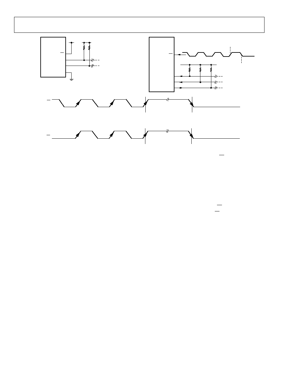
ADT7516/ADT7517/ADT7519
Rev. A | Page 38 of 44
ADT7516/
ADT7517/
ADT7519
CS
SDA
SCL
ADD
V
DD
V
DD
I
2
C ADDRESS = 1001 000
10k
10k
02883-A
-
057
Figure 57. Typical I
2
C Interface Connection
ADT7516/
ADT7517/
ADT7519
SCLK
DOUT
CS
V
DD
LOCK AND
SELECT SPI
SPI FRAMING
EDGE
820
820
820
DIN
02883-A
-
058
Figure 58. Typical SPI Interface Connection
A
B
CS
(START HIGH)
SPI LOCKED ON
THIRD RISING EDGE
C
SPI FRAMING
EDGE
02883-A
-
056
A
B
CS
(START LOW)
SPI LOCKED ON
THIRD RISING EDGE
C
SPI FRAMING
EDGE
Figure 59. Serial Interface--Selecting and Locking SPI Protocol
I
2
C Serial Interface
Like all I2C compatible devices, the ADT7516/ADT7517/
ADT7519 have a 7-bit serial address. The four MSBs of this
address for the ADT7516/ADT7517/ADT7519 are set to 1001.
The three LSBs are set by Pin 11, ADD. The ADD pin can be
configured three ways to give three different address options:
low, floating, and high. Setting the ADD pin low gives a serial
bus address of 1001 000, leaving it floating gives the address
1001 010, and setting it high gives the address 1001 011. The
recommended pull-up resistor value is 10 k.
There is an enable/disable bit for the SMBus timeout. When this
is enabled, the SMBus will time out after 25 ms of no activity. To
enable it, set Bit 6 of the Control Configuration 2 register. The
power-on default is with the SMBus timeout disabled.
The ADT7516/ADT7517/ADT7519 support SMBus packet
error checking (PEC), but its use is optional. It is triggered by
supplying the extra clocks for the PEC byte. The PEC is
calculated using CRC-8. The frame clock sequence (FCS)
conforms to CRC-8 by the polynominal
( )
1
1
2
8
+
+
+
=
x
x
x
x
C
Consult the SMBus specification (www.smbus.org) for more
information.
The serial bus protocol operates as follows:
1.
The master initiates a data transfer by establishing a start
condition, defined as a high to low transition on the serial
data line SDA while the serial clock line SCL remains high.
This indicates that an address/data stream will follow. All
slave peripherals connected to the serial bus respond to the
start condition and shift in the next eight bits, consisting of
a 7-bit address (MSB first) plus a R/W bit, which
determines the direction of the data transfer, i.e., whether
data will be written to or read from the slave device.
The peripheral whose address corresponds to the
transmitted address responds by pulling the data line low
during the low period before the ninth clock pulse, known
as the Acknowledge Bit. All other devices on the bus now
remain idle while the selected device waits for data to be
read from or written to it. If the R/W bit is 0 the master will
write to the slave device. If the R/W bit is 1, the master will
read from the slave device.
2.
Data is sent over the serial bus in sequences of nine clock
pulses: eight bits of data followed by an acknowledge bit
from the receiver of data. Transitions on the data line must
occur during the low period of the clock signal and remain
stable during the high period, because a low to high tran-
sition when the clock is high may be interpreted as a stop
signal.
3.
When all data bytes have been read or written, stop
conditions are established. In write mode, the master will
pull the data line high during the 10th clock pulse to assert
a stop condition. In read mode, the master device will pull
the data line high during the low period before the ninth
clock pulse. This is known as No Acknowledge. The master
will then take the data line low during the low period
before the 10th clock pulse, and then high during the 10th
clock pulse to assert a stop condition.
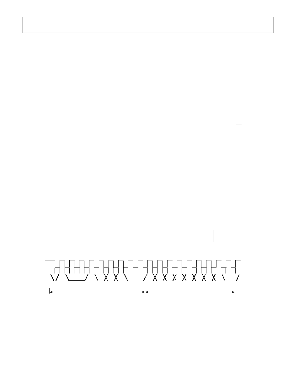
ADT7516/ADT7517/ADT7519
Rev. A | Page 39 of 44
Any number of bytes of data can be transferred over the serial
bus in one operation, but it is not possible to mix read and write
in one operation because the type of operation is determined at
the beginning and cannot subsequently be changed without
starting a new operation.
The I
2
C address set up by the ADD pin is not latched by the
device until after this address has been sent twice. On the eighth
SCL cycle of the second valid communication, the serial bus
address is latched in. This is the SCL cycle directly after the
device has seen its own I
2
C serial bus address. Any subsequent
changes on this pin will have no effect on the I
2
C serial bus
address.
Writing to the ADT7516/ADT7517/ADT7519
Depending on the register being written to, there are two
different writes for the ADT7516/ADT7517/ADT7519. It is not
possible to do a block write to this part, i.e., no I
2
C auto-
increment.
Writing to the Address Pointer Register for a
Subsequent Read
To read data from a particular register, the address pointer
register must contain the address of that register. If it does not,
the correct address must be written to the address pointer
register by performing a single-byte write operation, as shown
in Figure 60. The write operation consists of the serial bus
address followed by the address pointer byte. No data is written
to any of the data registers. A read operation is then performed
to read the register.
Writing Data to a Register
All registers are 8-bit registers, so only one byte of data can be
written to each register. Writing a single byte of data to one of
these read/write registers consists of the serial bus address, the
data register address written to the address pointer register,
followed by the data byte written to the selected data register.
This is illustrated in Figure 61. To write to a different register,
another start or repeated start is required. If more than one byte
of data is sent in one communication operation, the addressed
register will be repeatedly loaded until the last data byte has
been sent.
Reading Data from the ADT7516/ADT7517/ADT7519
Reading data from the ADT7516/ADT7517/ADT7519 is done
in a 1-byte operation. Reading back the contents of a register is
shown in Figure 62. The register address had previously been
set up by a single-byte write operation to the address pointer
register. To read from another register, write to the address
pointer register again to set up the relevant register address.
Thus, block reads are not possible, i.e., no I
2
C auto-increment.
SPI Serial Interface
The SPI serial interface of the ADT7516/ADT7517/ADT7519
consists of four wires: CS, SCLK, DIN, and DOUT. The CS is
used to select the device when more than one device is con-
nected to the serial clock and data lines. The CS is also used to
distinguish between any two separate serial communications
(see Figure 67 for a graphical explanation). The SCLK is used to
clock data in and out of the part. The D
IN
line is used to write to
the registers, and the DOUT line is used to read data back from
the registers. The recommended pull-up resistor value is
between 500 and 820 .
The part operates in slave mode and requires an externally
applied serial clock to the SCLK input. The serial interface is
designed to allow the part to be interfaced to systems that
provide a serial clock that is synchronized to the serial data.
There are two types of serial operations, read and write. Com-
mand words are used to distinguish read operations from write
operations. These command words are given in Table 67.
Address auto-increment is possible in SPI mode.
Table 67. SPI Command Words
Write
Read
90h (1001 0000)
91h (1001 0001)
0
1
R/W
SCL
SDA
FRAME 1
SERIAL BUS ADDRESS BYTE
FRAME 2
ADDRESS POINTER REGISTER BYTE
ACK. BY
ADT7516/ADT7517/ADT7519
ACK. BY
ADT7516/ADT7517/ADT7519
STOP BY
MASTER
START BY
MASTER
0
0
1
A2
A1
A
P7
P6
P5
P4
P3
P2
P1
P0
9
1
9
1
02883-A
-
059
Figure 60. I
2
C--Writing to the Address Pointer Register to Select a Register for a Subsequent Read Operation
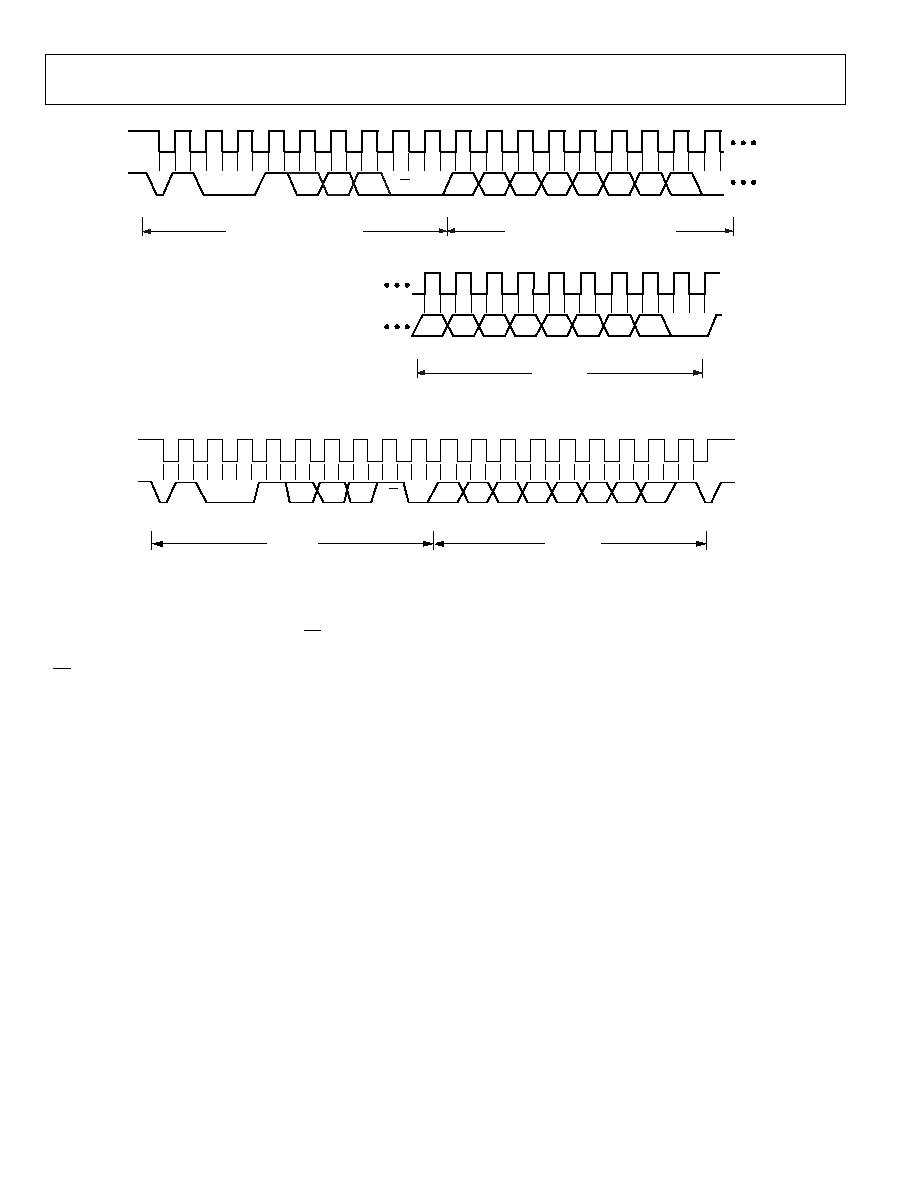
ADT7516/ADT7517/ADT7519
Rev. A | Page 40 of 44
FRAME 1
SERIAL BUS ADDRESS BYTE
FRAME 2
ADDRESS POINTER REGISTER BYTE
ACK. BY
ADT7516/ADT7517/ADT7519
ACK. BY
ADT7516/ADT7517/ADT7519
ACK. BY
ADT7516/ADT7517/ADT7519
STOP BY
MASTER
FRAME 3
DATA BYTE
SDA (CONTINUED)
SCL (CONTINUED)
SCL
SDA
START BY
MASTER
1
0
0
1
A2
A1
A0
P7
P6
P5
P4
P3
P2
P1
P0
9
D 7
D 6
D5
D 4
D3
D2
D1
D0
R/W
1
9
1
9
1
02883-A
-
060
Figure 61. I
2
C--Writing to the Address Pointer Register Followed by a Single Byte of Data to the Selected Register
1
SDA
START BY
MASTER
STOP BY
MASTER
NO ACK. BY
MASTER
ACK. BY
ADT7616/ADT7517/ADT7519
SCL
9
0
0
1
A2
A1
A0
R/W
D7
D6
D5
D4
D3
D2
D1
D0
FRAME 1
SERIAL BUS ADDRESS BYTE
FRAME 2
SINGLE DATA BYTE FROM ADT7516/ADT7517/ADT7519
1
9
1
02883-A
-
061
Figure 62. I
2
C--Reading a Single Byte of Data from a Selected Register
Write Operation
Figure 63 shows the timing diagram for a write operation to the
ADT7516/ADT7517/ADT7519. Data is clocked into the reg-
isters on the rising edge of SCLK. When the CS line is high, the
DIN and DOUT lines are in three-state mode. Only when the
CS goes from a high to a low does the part accept any data on
the DIN line. In SPI mode, the address pointer register is cap-
able of auto-incrementing to the next register in the register
map without having to load the address pointer register each
time. In Figure 63, the register address portion gives the first
register that will be written to. Subsequent data bytes will be
written into sequential writable registers. Thus, after each data
byte has been written into a register, the address pointer register
auto-increments its value to the next available register. The
address pointer register will auto-increment from 00h to 3Fh
and will loop back to start again at 00h when it reaches 3Fh.
Read Operation
Figure 64 to Figure 66 show the timing diagrams necessary to
accomplish correct read operations. To read back from a reg-
ister, first write to the address pointer register with the address
of the register to be read from. This operation is shown in
Figure 64. Figure 65 shows the procedure for reading back a
single byte of data. The read command is first sent to the part
during the first eight clock cycles. During the following eight
clock cycles, the data contained in the register selected by the
address pointer register is output onto the D
OUT
line. Data is
output onto the D
OUT
line on the falling edge of SCLK. Figure 66
shows the procedure when reading data from two sequential
registers. Multiple data reads are possible in the SPI interface
mode as the address pointer register is auto-incremental. The
address pointer register will auto-increment from 00h to 3Fh
and will loop back to start again at 00h when it reaches 3Fh
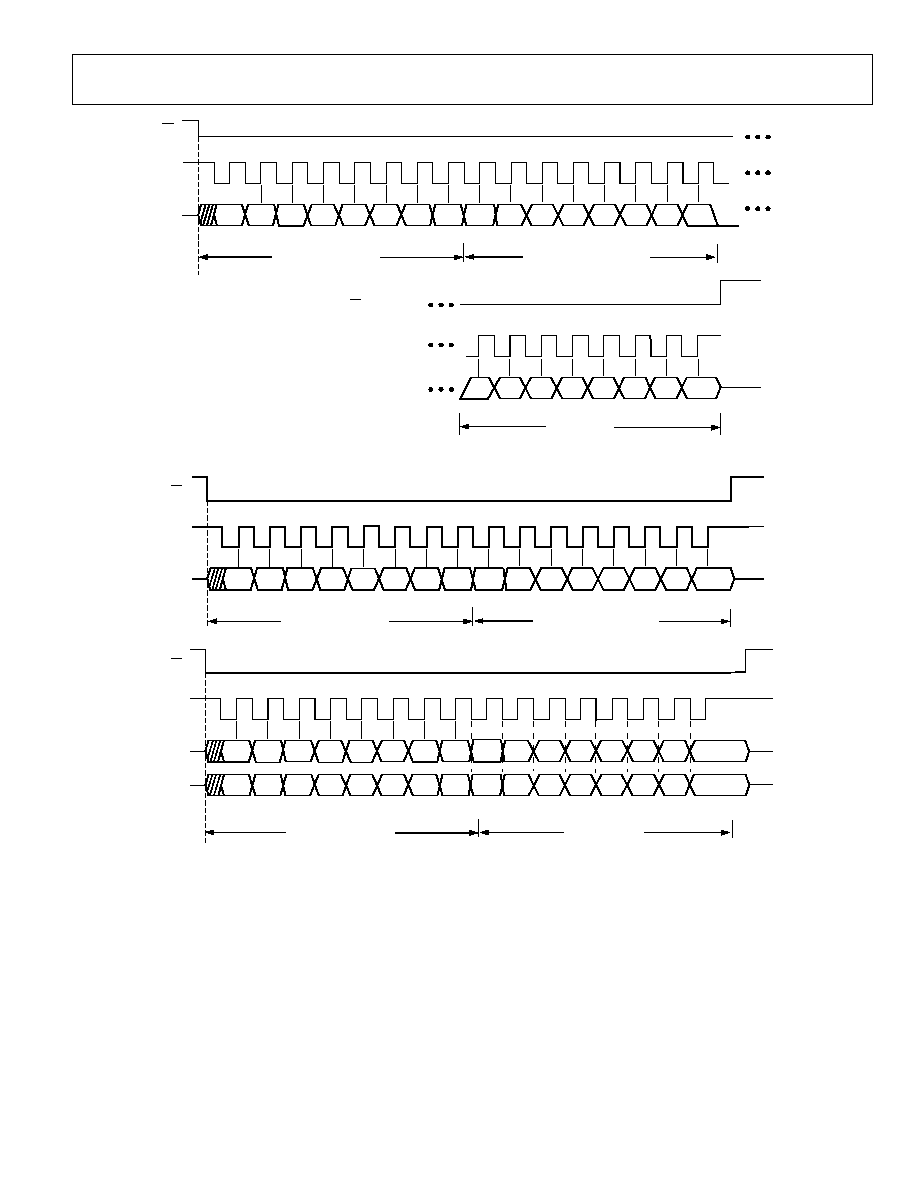
ADT7516/ADT7517/ADT7519
Rev. A | Page 41 of 44
D7
D6
D5
D4
D3
D2
D1
D6
D5
D4
D3
D2
D1
D0
D0
D7
1
8
1
8
CS
SCLK
DIN
STOP
D7
D6
D5
D4
D3
D2
D1
D0
1
8
CS (CONTINUED)
SCLK (CONTINUED)
DATA BYTE
REGISTER ADDRESS
WRITE COMMAND
DIN (CONTINUED)
02883-A
-
062
START
Figure 63. SPI--Writing to the Address Pointer Register Followed by a Single Byte of Data to the Selected Register
D7
DIN
D6
D5
D4
D3
D2
D1
D6
D5
D4
D3
D2
D1
D0
D0
D7
SCLK
1
8
1
8
CS
STOP
02883-A
-
063
WRITE COMMAND
START
REGISTER ADDRESS
Figure 64. SPI--Writing to the Address Pointer Register to Select a Register for a Subsequent Read Operation
D7
D6
D5
D4
D3
D2
D1
X
X
X
X
X
X
X
D0
X
CS
SCLK
DIN
DOUT
1
8
1
8
X
X
X
X
X
X
X
D6
D5
D4
D3
D2
D1
D0
X
D7
STOP
02883-A
-
064
DATA BYTE 1
READ COMMAND
START
Figure 65. SPI--Reading a Single Byte of Data From a Selected Register
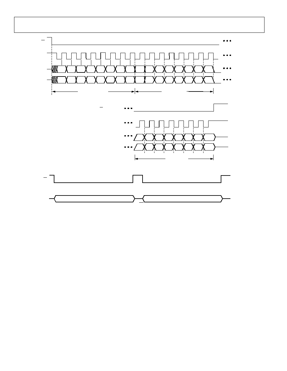
ADT7516/ADT7517/ADT7519
Rev. A | Page 42 of 44
D7
D6
D5
D4
D3
D2
D1
X
X
X
X
X
X
X
D0
X
CS
SCLK
DIN
DOUT
1
8
1
8
X
X
X
X
X
X
X
D6
D5
D4
D3
D2
D1
D0
X
D7
CS (CONTINUED)
SCLK (CONTINUED)
DIN (CONTINUED)
DOUT (CONTINUED)
STOP
X
X
X
X
X
X
X
X
1
8
D7
D6
D5
D4
D3
D2
D1
D0
02883-A
-
065
START
READ COMMAND
DATA BYTE 1
DATA BYTE 2
Figure 66. SPI--Reading Two Bytes of Data from Two Sequential Registers
CS
SPI
READ OPERATION
WRITE OPERATION
02883-A
-
066
Figure 67. SPI--Correct Use of CS during SPI Communication
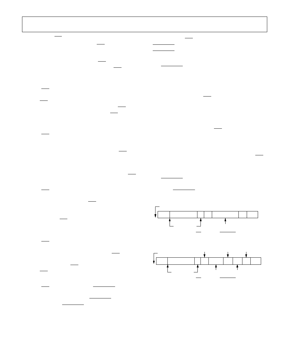
ADT7516/ADT7517/ADT7519
Rev. A | Page 43 of 44
SMBus/SPI INT/INT
The ADT7516/ADT7517/ADT7519 INT/INT outputs are an
interrupt line for devices that want to trade their ability to
master for an extra pin. The ADT7516/ADT7517/ADT7519 are
slave devices and use the SMBus/SPI INT/INT to signal the host
device that it wants to talk to. The SMBus/SPI INT/INT on the
ADT7516/ADT7517/ADT7519 is used as an over/under limit
indicator.
The INT/INT pin has an open-drain configuration that allows
the outputs of several devices to be wired-AND together when
the INT/INT pin is active low. Use C6 of the Control Config-
uration 1 register to set the active polarity of the INT/INT out-
put. The power-up default is active low. The INT/INT output
can be disabled or enabled by setting C5 of the Control Config-
uration 1 register to 1 or 0, respectively.
The INT/INT output becomes active when either the internal
temperature value, the external temperature value, V
DD
value, or
any of the AIN input values exceed the values in their corres-
ponding T
HIGH
/V
HIGH
or T
LOW
/V
LOW
registers. The INT/INT out-
put goes inactive again when a conversion result has the mea-
sured value back within the trip limits and when the status reg-
ister associated with the out-of-limit event is read. The two
interrupt status registers show which event caused the INT/INT
pin to go active.
The INT/INT output requires an external pull-up resistor. This
can be connected to a voltage different from V
DD
, provided the
maximum voltage rating of the INT/INT output pin is not
exceeded. The value of the pull-up resistor depends on the
application but should be large enough to avoid excessive sink
currents at the INT/INT output, which can heat the chip and
affect the temperature reading.
SMBUS ALERT RESPONSE
The INT/INT pin behaves the same way as an SMBus alert pin
when the SMBus/I
2
C interface is selected. It is an open-drain
output and requires a pull-up to V
DD
. Several INT/INT outputs
can be wire-AND together, so that the common line will go low
if one or more of the INT/INT outputs goes low. The polarity of
the INT/INT pin must be set active low for a number of outputs
to be wired-AND together.
The INT/INT output can operate as an SMBALERT function.
Slave devices on the SMBus can not normally signal to the
master that they want to talk, but the SMBALERT function
allows them to do so. SMBALERT is used in conjunction with
the SMBus general call address.
One or more INT/INT outputs can be connected to a common
SMBALERT line connected to the master. When the
SMBALERT line is pulled low by one of the devices, the
following procedure occurs as shown in Figure 68.
1.
SMBALERT pulled low.
2.
Master initiates a read operation and sends the alert res-
ponse address (ARA = 0001 100). This is a general call
address that must not be used as a specific device address.
3.
The devices whose INT/INT output is low responds to the
alert response address and the master reads its device
address. As the device address is seven bits long, an LSB of
1 is added. The address of the device is now known and it
can be interrogated in the usual way.
4.
If more than one device's INT/INT output is low, the one
with the lowest device address will have priority in accor-
dance with normal SMBus specifications.
5.
Once the ADT7516/ADT7517/ADT7519 have responded
to the alert response address, they will reset their INT/INT
output, provided that the condition that caused the out-of-
limit event no longer exists and that the status register
associated with the out-of-limit event is read. If the
SMBALERT line remains low, the master will send the
ARA again. It will continue to do this until all devices
whose SMBALERT outputs were low have responded.
MASTER
RECEIVES
SMBALERT
START ALERT RESPONSE
ADDRESS
RD ACK DEVICE ADDRESS
MASTER SENDS
ARA AND READ
COMMAND
DEVICE SENDS
ITS ADDRESS
NO
ACK STOP
02883-A
-
067
Figure 68. INT/INT Responds to SMBALERT ARA
MASTER
RECEIVES
SMBALERT
START ALERT RESPONSE
ADDRESS
RD ACK
DEVICE
ADDRESS
MASTER SENDS
ARA AND READ
COMMAND
DEVICE SENDS
ITS ADDRESS
DEVICE ACK
ACK
PEC
NO
ACK STOP
MASTER
ACK
MASTER
NACK
DEVICE SENDS
ITS PEC DATA
02883-
A-
068
Figure 69. INT/INT Responds to SMBALERT ARA
with Packet Error Checking (PEC)
ADT7516/ADT7517/ADT7519
Rev. A | Page 44 of 44
OUTLINE DIMENSIONS
16
9
8
1
PIN 1
SEATING
PLANE
0.010
0.004
0.012
0.008
0.025
BSC
0.010
0.006
0.050
0.016
8°
0°
COPLANARITY
0.004
0.065
0.049
0.069
0.053
0.154
BSC
0.236
BSC
COMPLIANT TO JEDEC STANDARDS MO-137AB
0.193
BSC
Figure 70. 16-Lead Shrink Small Outline Package [QSOP]
(RQ-16)
Dimensions in Inches
ORDERING GUIDE
Model
Temperature Range
DAC Resolution
Package Description
Minimum
Quantities/Reel
ADT7519ARQ
40°C to +120°C
8 Bits
16-Lead QSOP
N/A
ADT7519ARQ-REEL
40°C to +120°C
8 Bits
16-Lead QSOP
2500
ADT7519ARQ-REEL7
40°C to +120°C
8 Bits
16-Lead QSOP
1000
ADT7519ARQZ
1
40°C to +120°C
8 Bits
16-Lead QSOP
N/A
ADT7519ARQZ
1
-REEL
40°C to +120°C
8 Bits
16-Lead QSOP
2500
ADT7519ARQZ
1
-REEL7
40°C to +120°C
8 Bits
16-Lead QSOP
1000
ADT7517ARQ
40°C to +120°C
10 Bits
16-Lead QSOP
N/A
ADT7517ARQ-REEL
40°C to +120°C
10 Bits
16-Lead QSOP
2500
ADT7517ARQ-REEL7
40°C to +120°C
10 Bits
16-Lead QSOP
1000
ADT7516ARQ
40°C to +120°C
12 Bits
16-Lead QSOP
N/A
ADT7516ARQ-REEL
40°C to +120°C
12 Bits
16-Lead QSOP
2500
ADT7516ARQ-REEL7
40°C to +120°C
12 Bits
16-Lead QSOP
1000
1
Z = Pb-free part.
Purchase of licensed I
2
C components of Analog Devices or one of its sublicensed Associated Companies conveys a license for the purchaser under the Philips I
2
C
Patent Rights to use these components in an I
2
C system, provided that the system conforms to the I
2
C Standard Specification as defined by Philips.
© 2004 Analog Devices, Inc. All rights reserved. Trademarks and
registered trademarks are the property of their respective owners.
C02883-0-8/04(A)
Document Outline
- FEATURES
- APPLICATIONS
- PIN CONFIGURATION
- GENERAL DESCRIPTION
- þÿ
- þÿ
- þÿ
- þÿ
- þÿ
- þÿ
- þÿ
- þÿ