
050-7624 Rev A 11-2005
APT150GN60J
TYPICAL PERFORMANCE CURVES
MAXIMUM RATINGS
All Ratings: T
C
= 25∞C unless otherwise specified.
STATIC ELECTRICAL CHARACTERISTICS
Characteristic / Test Conditions
Collector-Emitter Breakdown Voltage (V
GE
= 0V, I
C
= 4mA)
Gate Threshold Voltage (V
CE
= V
GE
, I
C
= 2400µA, T
j
= 25∞C)
Collector-Emitter On Voltage (V
GE
= 15V, I
C
= 150A, T
j
= 25∞C)
Collector-Emitter On Voltage (V
GE
= 15V, I
C
= 150A, T
j
= 125∞C)
Collector Cut-off Current (V
CE
= 600V, V
GE
= 0V, T
j
= 25∞C)
2
Collector Cut-off Current (V
CE
= 600V, V
GE
= 0V, T
j
= 125∞C)
2
Gate-Emitter Leakage Current (V
GE
= ±20V)
Intergrated Gate Resistor
Symbol
V
(BR)CES
V
GE(TH)
V
CE(ON)
I
CES
I
GES
R
G(int)
Units
Volts
µA
nA
Symbol
V
CES
V
GE
I
C1
I
C2
I
CM
SSOA
P
D
T
J
,T
STG
T
L
APT150GN60J
600
±30
220
123
450
450A @ 600V
536
-55 to 175
300
UNIT
Volts
Amps
Watts
∞C
Parameter
Collector-Emitter Voltage
Gate-Emitter Voltage
Continuous Collector Current @ T
C
= 25∞C
Continuous Collector Current @ T
C
= 110∞C
Pulsed Collector Current
1
Switching Safe Operating Area @ T
J
= 175∞C
Total Power Dissipation
Operating and Storage Junction Temperature Range
Max. Lead Temp. for Soldering: 0.063" from Case for 10 Sec.
APT Website - http://www.advancedpower.com
CAUTION: These Devices are Sensitive to Electrostatic Discharge. Proper Handling Procedures Should Be Followed.
Utilizing the latest Field Stop and Trench Gate technologies, these IGBT's have ultra
low V
CE(ON)
and are ideal for low frequency applications that require absolute minimum
conduction loss. Easy paralleling is a result of very tight parameter distribution and
a slightly positive V
CE(ON)
temperature coefficient. A built-in gate resistor ensures
extremely reliable operation, even in the event of a short circuit fault. Low gate charge
simplifies gate drive design and minimizes losses.
∑
600V Field Stop
∑ Trench Gate: Low V
CE(on)
∑ Easy Paralleling
∑ Intergrated Gate Resistor: Low EMI, High Reliability
Applications: Welding, Inductive Heating, Solar Inverters, SMPS, Motor drives, UPS
MIN
TYP
MAX
600
5.0
5.8
6.5
1.05
1.45
1.85
1.65
25
TBD
600
2
Æ
G
C
E
600V
APT150GN60J
SO
T-2
27
ISOTOP
Æ
file # E145592
"UL Recognized"
G
E
E
C

050-7624 Rev A 11-2005
APT150GN60J
1
Repetitive Rating: Pulse width limited by maximum junction temperature.
2
For Combi devices, I
ces
includes both IGBT and FRED leakages
3
See MIL-STD-750 Method 3471.
4
E
on1
is the clamped inductive turn-on energy of the IGBT only, without the effect of a commutating diode reverse recovery current
adding to the IGBT turn-on loss. Tested in inductive switching test circuit shown in figure 21, but with a Silicon Carbide diode.
5
E
on2
is the clamped inductive turn-on energy that includes a commutating diode reverse recovery current in the IGBT turn-on switching
loss. (See Figures 21, 22.)
6
E
off
is the clamped inductive turn-off energy measured in accordance with JEDEC standard JESD24-1. (See Figures 21, 23.)
7 R
G
is external gate resistance, not including R
G(int)
nor gate driver impedance. (MIC4452)
APT Reserves the right to change, without notice, the specifications and information contained herein.
DYNAMIC CHARACTERISTICS
Symbol
C
ies
C
oes
C
res
V
GEP
Q
g
Q
ge
Q
gc
SSOA
t
d(on)
t
r
t
d(off)
t
f
E
on1
E
on2
E
off
t
d(on)
t
r
t
d(off)
t
f
E
on1
E
on2
E
off
Test Conditions
Capacitance
V
GE
= 0V, V
CE
= 25V
f = 1 MHz
Gate Charge
V
GE
= 15V
V
CE
= 300V
I
C
= 150A
T
J
= 175∞C, R
G
= 4.3
7
, V
GE
=
15V, L = 100µH,V
CE
= 600V
Inductive Switching (25∞C)
V
CC
= 400V
V
GE
= 15V
I
C
= 150A
R
G
= 1.0
7
T
J
= +25∞C
Inductive Switching (125∞C)
V
CC
= 400V
V
GE
= 15V
I
C
= 150A
R
G
= 1.0
7
T
J
= +125∞C
Characteristic
Input Capacitance
Output Capacitance
Reverse Transfer Capacitance
Gate-to-Emitter Plateau Voltage
Total Gate Charge
3
Gate-Emitter Charge
Gate-Collector ("Miller") Charge
Switching Safe Operating Area
Turn-on Delay Time
Current Rise Time
Turn-off Delay Time
Current Fall Time
Turn-on Switching Energy
4
Turn-on Switching Energy (Diode)
5
Turn-off Switching Energy
6
Turn-on Delay Time
Current Rise Time
Turn-off Delay Time
Current Fall Time
Turn-on Switching Energy
4
4
Turn-on Switching Energy (Diode)
5
5
Turn-off Switching Energy
6
6
MIN
TYP
MAX
9200
350
300
9.5
970
65
510
450
44
110
430
60
8810
8615
4295
44
110
480
95
8880
9735
5460
UNIT
pF
V
nC
A
ns
µ
J
ns
µ
J
THERMAL AND MECHANICAL CHARACTERISTICS
UNIT
∞C/W
Volts
oz
gm
Ib∑in
N∑m
MIN
TYP
MAX
0.28
N/A
2500
1.03
29.2
10
1.1
Characteristic
Junction to Case
(IGBT)
Junction to Case
(DIODE)
RMS Voltage (
50-60Hz Sinusoidal Waveform from Terminals to Mounting Base for 1 Min.)
Package Weight
Maximum Terminal & Mounting Torque
Symbol
R
JC
R
JC
V
Isolation
W
T
Torque

050-7624 Rev A 11-2005
APT150GN60J
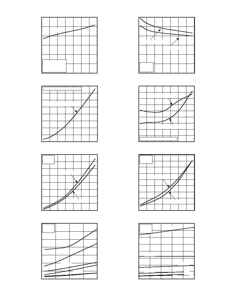
TYPICAL PERFORMANCE CURVES
V
GS(TH)
, THRESHOLD VOLTAGE
V
CE
, COLLECTOR-TO-EMITTER VOLTAGE (V)
I
C
, COLLECTOR CURRENT (A)
I
C
, COLLECTOR CURRENT (A)
(NORMALIZED)
I
C,
DC COLLECTOR CURRENT(A)
V
CE
, COLLECTOR-TO-EMITTER VOLTAGE (V)
V
GE
, GATE-TO-EMITTER VOLTAGE (V)
I
C
, COLLECTOR CURRENT (A)
250µs PULSE
TEST<0.5 % DUTY
CYCLE
350
300
250
200
150
100
50
0
350
300
250
200
150
100
50
0
4.0
3.5
3.0
2.5
2.0
1.5
1.0
0.5
0
1.15
1.10
1.05
1.00
0.95
0.90
0.85
0.80
0.75
0.70
0
0.5 1.0
1.5 2.0
2.5 3.0
3.5
0
5
10
15
20
25
30
0
2
4
6
8
10
12
14
0
200
400
600
800 1000 1200
8
10
12
14
16
0
25
50
75 100 125 150 175
-50 -25
0
25 50
75 100 125 150
-50 -25 0 25 50 75 100 125 150 175
400
350
300
250
200
150
100
50
0
16
14
12
10
8
6
4
2
0
3.0
2.5
2.0
1.5
1.0
0.5
0
300
250
200
150
100
50
0
V
CE
, COLLECTER-TO-EMITTER VOLTAGE (V)
V
CE
, COLLECTER-TO-EMITTER VOLTAGE (V)
FIGURE 1, Output Characteristics(T
J
= 25∞C)
FIGURE 2, Output Characteristics (T
J
= 125∞C)
V
GE
, GATE-TO-EMITTER VOLTAGE (V)
GATE CHARGE (nC)
FIGURE 3, Transfer Characteristics
FIGURE 4, Gate Charge
V
GE
, GATE-TO-EMITTER VOLTAGE (V)
T
J
, Junction Temperature (∞C)
FIGURE 5, On State Voltage vs Gate-to- Emitter Voltage
FIGURE 6, On State Voltage vs Junction Temperature
T
J
, JUNCTION TEMPERATURE (∞C)
T
C
, CASE TEMPERATURE (∞C)
FIGURE 7, Threshold Voltage vs. Junction Temperature
FIGURE 8, DC Collector Current vs Case Temperature
12, 13 &15V
9V
8V
7V
11V
T
J
= 125∞C
T
J
= 25∞C
T
J
= -55∞C
V
GE
= 15V.
250µs PULSE TEST
<0.5 % DUTY CYCLE
T
J
= 125∞C
T
J
= 25∞C
T
J
= -55∞C
T
J
= 175∞C
V
GE
= 15V
10V
V
CE
= 300V
V
CE
= 120V
I
C
= 150A
T
J
= 25∞C
V
CE
= 480V
T
J
= 25∞C.
250µs PULSE TEST
<0.5 % DUTY CYCLE
I
C
= 300A
I
C
= 150A
I
C
= 75A
I
C
= 300A
I
C
= 150A
I
C
= 75A
T
J
= 175∞C
050-7624 Rev A 11-2005
APT150GN60J
V
GE
=15V,T
J
=125∞C
V
GE
=15V,T
J
=25∞C
V
CE
=
400V
R
G
=
1.0
L = 100µH
SWITCHING ENERGY LOSSES (µJ)
E
ON2
, TURN ON ENERGY LOSS (µJ)
t
r,
RISE TIME (ns)
t
d(ON)
, TURN-ON DELAY TIME (ns)
SWITCHING ENERGY LOSSES (µJ)
E
OFF
, TURN OFF ENERGY LOSS (µJ)
t
f,
FALL TIME (ns)
t
d
(OFF)
, TURN-OFF DELAY TIME (ns)
I
CE
, COLLECTOR TO EMITTER CURRENT (A)
I
CE
, COLLECTOR TO EMITTER CURRENT (A)
FIGURE 9, Turn-On Delay Time vs Collector Current
FIGURE 10, Turn-Off Delay Time vs Collector Current
I
CE
, COLLECTOR TO EMITTER CURRENT (A)
I
CE
, COLLECTOR TO EMITTER CURRENT (A)
FIGURE 11, Current Rise Time vs Collector Current
FIGURE 12, Current Fall Time vs Collector Current
I
CE
, COLLECTOR TO EMITTER CURRENT (A)
I
CE
, COLLECTOR TO EMITTER CURRENT (A)
FIGURE 13, Turn-On Energy Loss vs Collector Current
FIGURE 14, Turn Off Energy Loss vs Collector Current
R
G
, GATE RESISTANCE (OHMS)
T
J
, JUNCTION TEMPERATURE (∞C)
FIGURE 15, Switching Energy Losses vs. Gate Resistance
FIGURE 16, Switching Energy Losses vs Junction Temperature
V
CE
= 400V
T
J
= 25∞C
,
or
125∞C
R
G
= 1.0
L = 100µH
60
50
40
30
20
10
0
400
350
300
250
200
150
100
50
0
40,000
35,000
30,000
25,000
20,000
15,000
10,000
5,000
0
70,000
60,000
50,000
40,000
30,000
20,000
10,000
0
600
500
400
300
200
100
0
180
160
140
120
100
80
60
40
20
0
18,000
16,000
14,000
12,000
10,000
8,000
6,000
4,000
2,000
0
40,000
35,000
30,000
25,000
20,000
15,000
10,000
5,000
0
V
GE
= 15V
T
J
=
125∞C, V
GE
=
15V
T
J
=
25∞C, V
GE
=
15V
V
CE
= 400V
V
GE
= +15V
R
G
= 1.0
30
70
110 150 190 230 270 310
30
70
110 150 190 230 270 310
30
70 110 150 190 230 270 310
30
70 110 150 190 230 270 310
30
70 110 150 190 230 270 310
30
70 110 150 190 230 270 310
0
5
10
15
20
0
25
50
75
100
125
R
G
=
1.0, L
=
100
µ
H, V
CE
=
400V
R
G
=
1.0, L
=
100
µ
H, V
CE
=
400V
T
J
=
25 or 125∞C,V
GE
=
15V
V
CE
= 400V
V
GE
= +15V
R
G
= 1.0
T
J
=
125∞C
T
J
=
25∞C
V
CE
= 400V
V
GE
= +15V
R
G
= 1.0
T
J
=
125∞C
T
J
=
25∞C
E
on2,
300A
E
off,
300A
E
on2,
150A
E
off,
150A
E
on2,
75A
E
off,
75A
V
CE
= 400V
V
GE
= +15V
T
J
= 125∞C
E
on2,
300A
E
off,
300A
E
on2,
150A
E
off,
150A
E
on2,
75A
E
off,
75A
050-7624 Rev A 11-2005
APT150GN60J
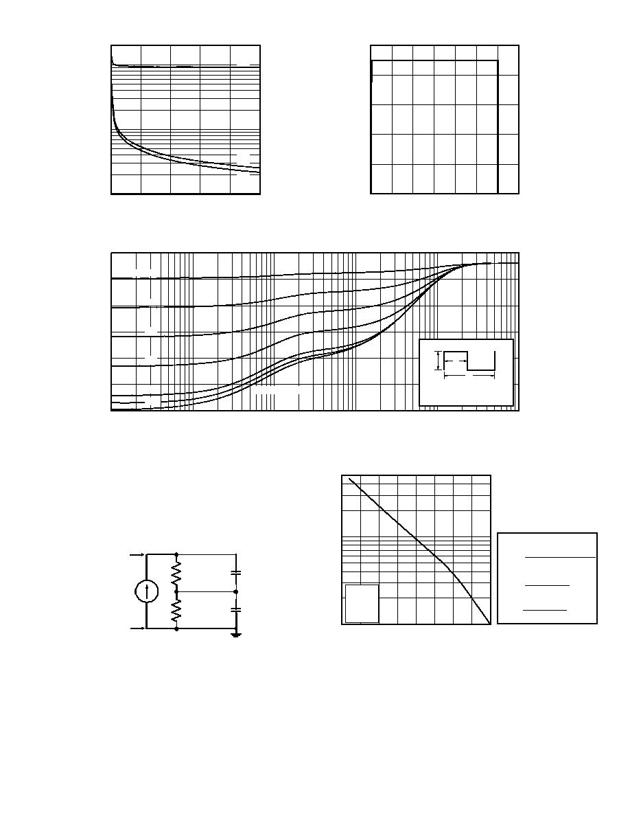
TYPICAL PERFORMANCE CURVES
0.30
0.25
0.20
0.15
0.10
0.05
0
Z
JC
, THERMAL IMPEDANCE (∞C/W)
0.3
D = 0.9
0.7
SINGLE PULSE
RECTANGULAR PULSE DURATION (SECONDS)
Figure 19a, Maximum Effective Transient Thermal Impedance, Junction-To-Case vs Pulse Duration
10
-5
10
-4
10
-3
10
-2
10
-1
1.0
20,000
10,000
500
100
50
10
500
400
300
200
100
0
C, CAPACITANCE (
P
F)
I
C
, COLLECTOR CURRENT (A)
V
CE
, COLLECTOR-TO-EMITTER VOLTAGE (VOLTS)
V
CE
, COLLECTOR TO EMITTER VOLTAGE
Figure 17, Capacitance vs Collector-To-Emitter Voltage
Figure 18,Minimim Switching Safe Operating Area
0
10
20
30
40
50
0
100 200 300 400 500 600 700
FIGURE 19b, TRANSIENT THERMAL IMPEDANCE MODEL
30 50 70 90 110 130 150 170 190
F
MAX
, OPERATING FREQUENCY (kHz)
I
C
, COLLECTOR CURRENT (A)
Figure 20, Operating Frequency vs Collector Current
T
J
= 125
∞
C
T
C
= 75
∞
C
D = 50 %
V
CE
= 400V
R
G
= 1.0
50
10
5
1
0.5
0.1
0.05
F
max
=
min (f
max
, f
max2
)
0.05
f
max1
=
t
d(on)
+ t
r
+ t
d(off)
+ t
f
P
diss
- P
cond
E
on2
+ E
off
f
max2
=
P
diss
=
T
J
- T
C
R
JC
Peak TJ = PDM x ZJC + TC
Duty Factor D =
t1
/
t2
t2
t1
P
DM
Note:
C
res
C
oes
C
ies
0.0964
0.184
0.00770
0.300
Power
(watts)
RC MODEL
Junction
temp. (∞C)
Case temperature. (∞C)
050-7624 Rev A 11-2005
APT150GN60J
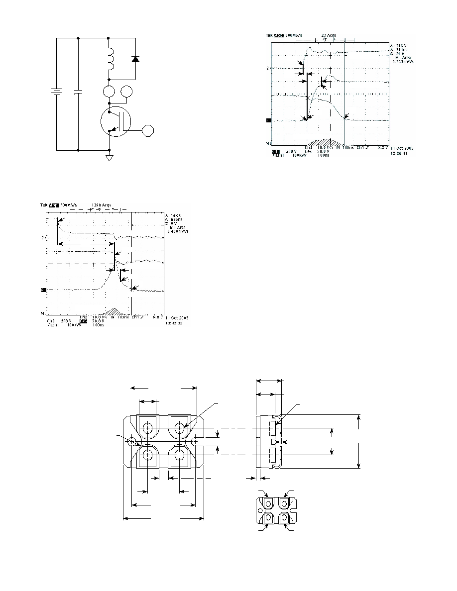
Figure 22, Turn-on Switching Waveforms and Definitions
Figure 23, Turn-off Switching Waveforms and Definitions
T
J
= 125∞C
Collector Current
Collector Voltage
Gate Voltage
Switching Energy
5%
10%
t
d(on)
90%
10%
t
r
5%
T
J
= 125∞C
Collector Voltage
Collector Current
Gate Voltage
Switching Energy
0
90%
t
d(off)
10%
t
f
90%
APT100DQ60
SOT-227 (ISOTOP
Æ)
Package Outline
APT's products are covered by one or more of U.S.patents 4,895,810 5,045,903 5,089,434 5,182,234 5,019,522
5,262,336 6,503,786 5,256,583 4,748,103 5,283,202 5,231,474 5,434,095 5,528,058 and foreign patents. US and Foreign patents pending. All Rights Reserved.
ISOTOP
Æ
is a Registered Trademark of SGS Thomson.
31.5 (1.240)
31.7 (1.248)
Dimensions in Millimeters and (Inches)
7.8 (.307)
8.2 (.322)
30.1 (1.185)
30.3 (1.193)
38.0 (1.496)
38.2 (1.504)
14.9 (.587)
15.1 (.594)
11.8 (.463)
12.2 (.480)
8.9 (.350)
9.6 (.378)
Hex Nut M4
(4 places)
0.75 (.030)
0.85 (.033)
12.6 (.496)
12.8 (.504)
25.2 (0.992)
25.4 (1.000)
1.95 (.077)
2.14 (.084)
* Emitter
Collector
Gate
*
r = 4.0 (.157)
(2 places)
4.0 (.157)
4.2 (.165)
(2 places)
W=4.1 (.161)
W=4.3 (.169)
H=4.8 (.187)
H=4.9 (.193)
(4 places)
3.3 (.129)
3.6 (.143)
* Emitter
Emitter terminals are shorted
internally. Current handling
capability is equal for either
Source terminal.
I
C
A
D.U.T.
V
CE
Figure 21, Inductive Switching Test Circuit
V
CC