050-7426 Rev B 11-2003
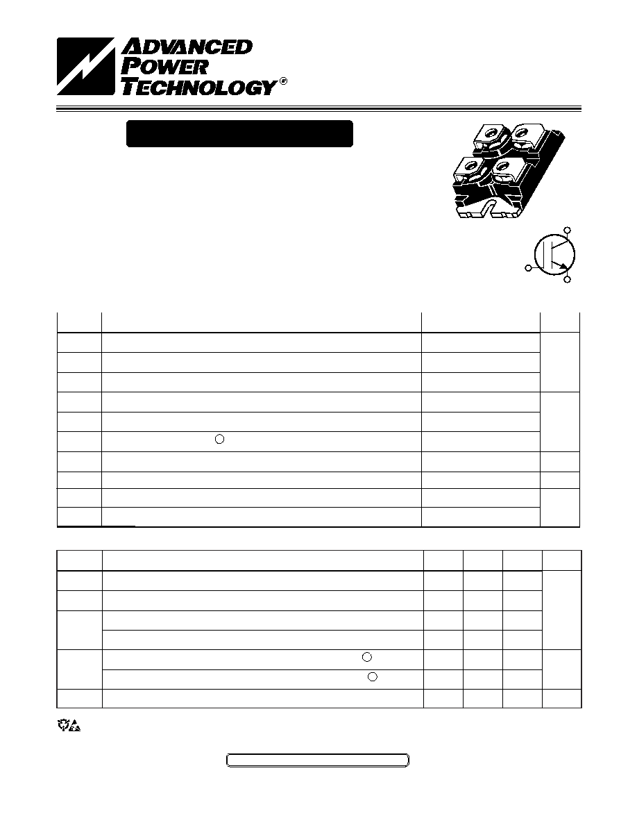
SOT-227
G
E
E
C
ISOTOP
Æ
"UL Recognized"
APT80GP60J
600V
MAXIMUM RATINGS
All Ratings: T
C
= 25∞C unless otherwise specified.
CAUTION: These Devices are Sensitive to Electrostatic Discharge. Proper Handling Procedures Should Be Followed.
APT Website - http://www.advancedpower.com
STATIC ELECTRICAL CHARACTERISTICS
MIN
TYP
MAX
600
3
4.5
6
2.2
2.7
2.1
1.0
5
±100
Symbol
BV
CES
V
GE(TH)
V
CE(ON)
I
CES
I
GES
UNIT
Volts
mA
nA
Symbol
V
CES
V
GE
V
GEM
I
C1
I
C2
I
CM
SSOA
P
D
T
J
,T
STG
T
L
APT80GP60J
600
±20
±30
151
68
330
330A @ 600V
462
-55 to 150
300
UNIT
Volts
Amps
Watts
∞C
Parameter
Collector-Emitter Voltage
Gate-Emitter Voltage
Gate-Emitter Voltage Transient
Continuous Collector Current @ T
C
= 25∞C
Continuous Collector Current @ T
C
= 110∞C
Pulsed Collector Current
1
@ T
C
= 25∞C
Switching Safe Operating Area @ T
J
= 150∞C
Total Power Dissipation
Operating and Storage Junction Temperature Range
Max. Lead Temp. for Soldering: 0.063" from Case for 10 Sec.
Characteristic / Test Conditions
Collector-Emitter Breakdown Voltage (V
GE
= 0V, I
C
= 1.0mA)
Gate Threshold Voltage (V
CE
= V
GE
, I
C
= 2.5mA, T
j
= 25∞C)
Collector-Emitter On Voltage (V
GE
= 15V, I
C
= 80A, T
j
= 25∞C)
Collector-Emitter On Voltage (V
GE
= 15V, I
C
= 80A, T
j
= 125∞C)
Collector Cut-off Current (V
CE
= 600V, V
GE
= 0V, T
j
= 25∞C)
2
Collector Cut-off Current (V
CE
= 600V, V
GE
= 0V, T
j
= 125∞C)
2
Gate-Emitter Leakage Current (V
GE
= ±20V)
The POWER MOS 7
Æ
IGBT is a new generation of high voltage power IGBTs.
Using Punch Through Technology this IGBT is ideal for many high frequency,
high voltage switching applications and has been optimized for high frequency
switchmode power supplies.
∑ Low Conduction Loss
∑ 100 kHz operation @ 400V, 39A
∑ Low Gate Charge
∑ 50 kHz operation @ 400V, 59A
∑ Ultrafast Tail Current shutoff
∑ SSOA rated
POWER MOS 7
Æ
IGBT
G
C
E
050-7426 Rev B 11-2003
APT80GP60J
DYNAMIC CHARACTERISTICS
Symbol
C
ies
C
oes
C
res
V
GEP
Q
g
Q
ge
Q
gc
SSOA
t
d(on)
t
r
t
d(off)
t
f
E
on1
E
on2
E
off
t
d(on)
t
r
t
d(off)
t
f
E
on1
E
on2
E
off
Test Conditions
Capacitance
V
GE
= 0V, V
CE
= 25V
f = 1 MHz
Gate Charge
V
GE
= 15V
V
CE
= 300V
I
C
= 80A
T
J
= 150∞C, R
G
= 5
,
V
GE
=
15V, L = 100µH,V
CE
= 600V
Inductive Switching (25∞C)
V
CC
= 400V
V
GE
= 15V
I
C
= 80A
R
G
= 5
T
J
= +25∞C
Inductive Switching (125∞C)
V
CC
= 400V
V
GE
= 15V
I
C
= 80A
R
G
= 5
T
J
= +125∞C
Characteristic
Input Capacitance
Output Capacitance
Reverse Transfer Capacitance
Gate-to-Emitter Plateau Voltage
Total Gate Charge
3
Gate-Emitter Charge
Gate-Collector ("Miller") Charge
Switching SOA
Turn-on Delay Time
Current Rise Time
Turn-off Delay Time
Current Fall Time
Turn-on Switching Energy
4
Turn-on Switching Energy (Diode)
5
Turn-off Switching Energy
6
Turn-on Delay Time
Current Rise Time
Turn-off Delay Time
Current Fall Time
Turn-on Switching Energy
4
Turn-on Switching Energy (Diode)
5
Turn-off Switching Energy
6
MIN
TYP
MAX
9840
735
40
7.5
280
65
85
330
29
40
116
78
795
1536
1199
29
40
149
84
795
2153
1690
UNIT
pF
V
nC
A
ns
µ
J
ns
µ
J
UNIT
∞C/W
gm
MIN
TYP
MAX
.27
N/A
29.2
Characteristic
Junction to Case (IGBT)
Junction to Case (DIODE)
Package Weight
Symbol
R
JC
R
JC
W
T
THERMAL AND MECHANICAL CHARACTERISTICS
1 Repetitive Rating: Pulse width limited by maximum junction temperature.
2 For Combi devices, I
ces
includes both IGBT and FRED leakages
3 See MIL-STD-750 Method 3471.
4 E
on1
is the clamped inductive turn-on-energy of the IGBT only, without the effect of a commutating diode reverse recovery current
adding to the IGBT turn-on loss. (See Figure 24.)
5 E
on2
is the clamped inductive turn-on energy that includes a commutating diode reverse recovery current in the IGBT turn-on switching
loss. A Combi device is used for the clamping diode as shown in the E
on2
test circuit. (See Figures 21, 22.)
6 E
off
is the clamped inductive turn-off energy measured in accordance with JEDEC standard JESD24-1. (See Figures 21, 23.)
APT Reserves the right to change, without notice, the specifications and information contained herein.
050-7426 Rev B 11-2003
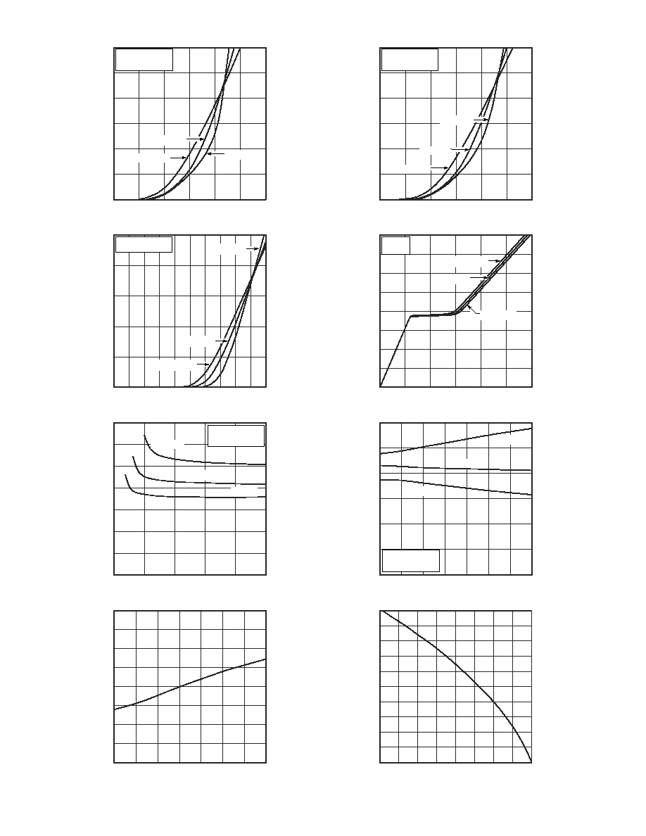
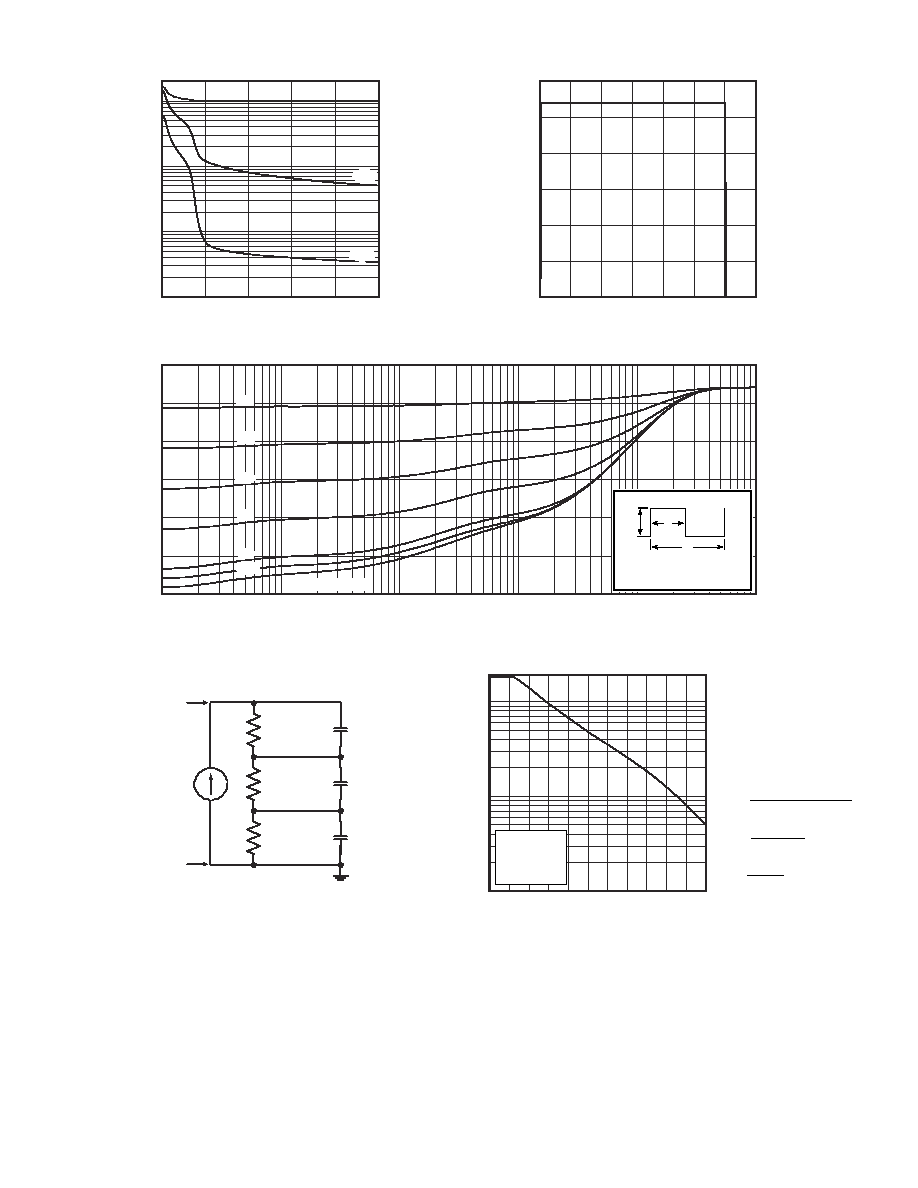
TYPICAL PERFORMANCE CURVES
APT80GP60J
V
CE
, COLLECTER-TO-EMITTER VOLTAGE (V)
V
CE
, COLLECTER-TO-EMITTER VOLTAGE (V)
FIGURE 1, Output Characteristics(V
GE
= 15V)
FIGURE 2, Output Characteristics (V
GE
= 10V)
V
GE
, GATE-TO-EMITTER VOLTAGE (V)
GATE CHARGE (nC)
FIGURE 3, Transfer Characteristics
FIGURE 4, Gate Charge
V
GE
, GATE-TO-EMITTER VOLTAGE (V)
T
J
, Junction Temperature (∞C)
FIGURE 5, On State Voltage vs Gate-to- Emitter Voltage
FIGURE 6, On State Voltage vs Junction Temperature
T
J
, JUNCTION TEMPERATURE (∞C)
T
C
, CASE TEMPERATURE (∞C)
FIGURE 7, Breakdown Voltage vs. Junction Temperature
FIGURE 8, DC Collector Current vs Case Temperature
BV
CES
, COLLECTOR-TO-EMITTER BREAKDOWN
V
CE
, COLLECTOR-TO-EMITTER VOLTAGE (V)
I
C
, COLLECTOR CURRENT (A)
I
C
, COLLECTOR CURRENT (A)
VOLTAGE (NORMALIZED)
I
C,
DC COLLECTOR CURRENT(A)
V
CE
, COLLECTOR-TO-EMITTER VOLTAGE (V)
V
GE
, GATE-TO-EMITTER VOLTAGE (V)
I
C
, COLLECTOR CURRENT (A)
0
0.5
1
1.5
2
2.5
3
0
0.5
1
1.5
2
2.5
3
0
1
2
3
4
5
6
7
8
9
10
0
50
100
150
200
250
300
6
8
10
12
14
16
-50
-25
0
25
50
75
100
125
-50
-25
0
25
50
75
100 125
-50
-25
0
25
50
75 100 125 150
TJ = 25∞C.
250µs PULSE TEST
<0.5 % DUTY CYCLE
T
C
=-55∞C
T
C
=125∞C
T
C
=25∞C
V
CE
=480V
V
CE
=300V
V
CE
=120V
VGE = 10V.
250µs PULSE TEST
<0.5 % DUTY CYCLE
VGE = 15V.
250µs PULSE TEST
<0.5 % DUTY CYCLE
VGE = 15V.
250µs PULSE TEST
<0.5 % DUTY CYCLE
IC = 80A
TJ = 25∞C
TJ = 25∞C
TJ = -55∞C
TJ = 125∞C
T
C
=-55∞C
T
C
=25∞C
T
C
=125∞C
250µs PULSE TEST
<0.5 % DUTY CYCLE
I
C=
40A
I
C=
80A
I
C=
160A
I
C=
160A
I
C=
80A
I
C=
40A
120
100
80
60
40
20
0
500
400
300
200
100
0
3.5
3
2.5
2
1.5
1
0.5
0
1.2
1.15
1.10
1.05
1.0
0.95
0.9
0.85
0.8
120
100
80
60
40
20
0
16
14
12
10
8
6
4
2
0
3
2.5
2
1.5
1
0.5
0
200
160
120
80
40
0
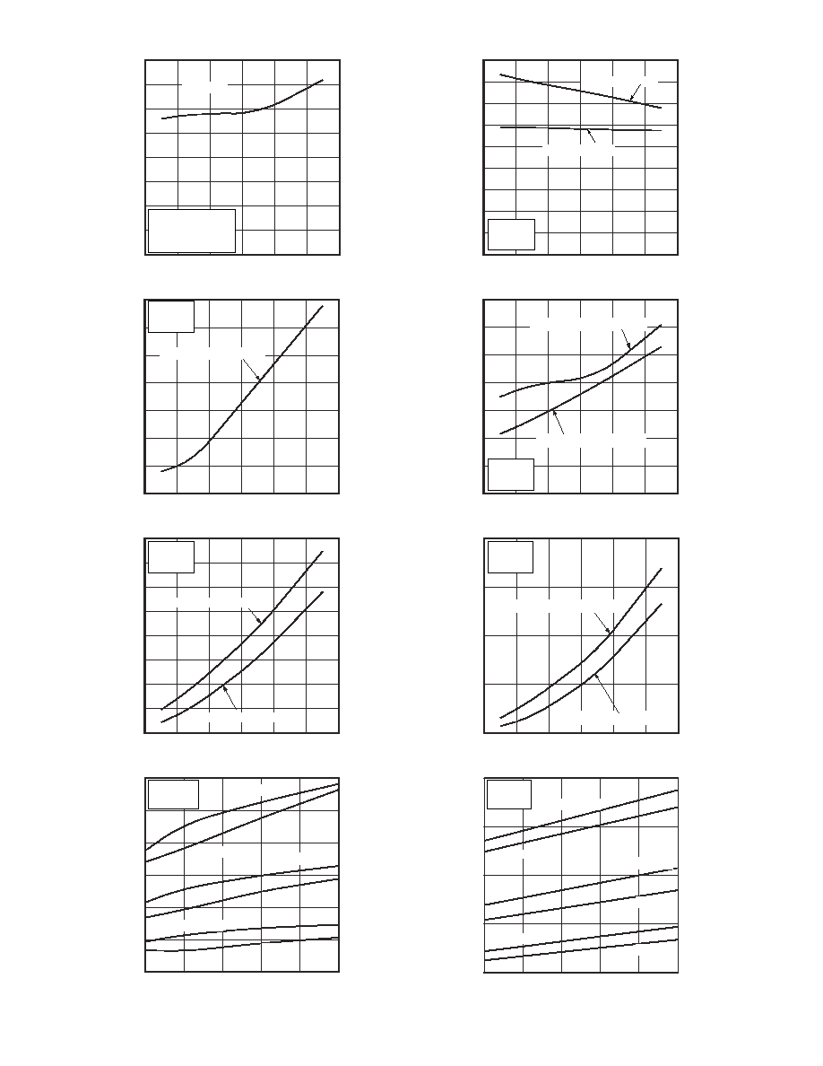
050-7426 Rev B 11-2003
APT80GP60J
T
J
=
125∞C, V
GE
=
10V
or 15V
T
J
=
25∞C, V
GE
=
10V
or 15V
V
GE
=
15V,T
J
=125∞C
V
GE
= 15V
V
GE
=
15V,T
J
=25∞C
T
J
=
25∞C, V
GE
=
10V
or 15V
I
CE
, COLLECTOR TO EMITTER CURRENT (A)
I
CE
, COLLECTOR TO EMITTER CURRENT (A)
FIGURE 9, Turn-On Delay Time vs Collector Current
FIGURE 10, Turn-Off Delay Time vs Collector Current
I
CE
, COLLECTOR TO EMITTER CURRENT (A)
I
CE
, COLLECTOR TO EMITTER CURRENT (A)
FIGURE 11, Current Rise Time vs Collector Current
FIGURE 12, Current Fall Time vs Collector Current
I
CE
, COLLECTOR TO EMITTER CURRENT (A)
I
CE
, COLLECTOR TO EMITTER CURRENT (A)
FIGURE 13, Turn-On Energy Loss vs Collector Current
FIGURE 14, Turn Off Energy Loss vs Collector Current
R
G
, GATE RESISTANCE (OHMS)
T
J
, JUNCTION TEMPERATURE (∞C)
FIGURE 15, Switching Energy Losses vs. Gate Resistance
FIGURE 16, Switching Energy Losses vs Junction Temperature
E
on2
40A
E
off
80A
E
on2
80A
E
on2
120A
E
off
120A
E
off
40A
E
on2
40A
E
off
80A
E
on2
80A
E
on2
120A
E
off
120A
E
off
40A
T
J
=
25 or 125∞C,V
GE
=
15V
SWITCHING ENERGY LOSSES (µJ)
E
ON2
, TURN ON ENERGY LOSS (µJ)
t
r,
RISE TIME (ns)
t
d(ON)
, TURN-ON DELAY TIME (ns)
SWITCHING ENERGY LOSSES (µJ)
E
OFF
, TURN OFF ENERGY LOSS (µJ)
t
f,
FALL TIME (ns)
t
d
(OFF)
, TURN-OFF DELAY TIME (ns)
T
J
=125∞C, V
GE
=15V
T
J
=
125∞C, V
GE
=
10V
or 15V
T
J
= 25∞C, V
GE
=15V
V
CE
= 400V
T
J
=
25∞C
,
T
J
=125∞C
R
G
= 5
L = 100 µH
V
CE
= 400V
R
G
=
5
L = 100 µH
10
30
50
70
90
110
130
10
30
50
70
90
110
130
10
30
50
70
90
110
130
10
30
50
70
90
110
130
10
30
50
70
90
110
130
10
30
50
70
90
110
130
5
10
15
20
25
30
0
25
50
75
100
125
VCE = 400V
VGE = +15V
RG = 5
40
35
30
25
20
15
10
5
0
70
60
50
40
30
20
10
0
4000
3500
3000
2500
2000
1500
1000
500
0
6000
5000
4000
3000
2000
1000
0
VCE = 400V
VGE = +15V
T
J
= 125∞C
V
CE
= 400V
R
G
=
5
L = 100 µH
V
CE
= 400V
R
G
=
5
L = 100 µH
180
160
140
120
100
80
60
40
20
0
140
120
100
80
60
40
20
0
4000
3000
2000
1000
0
4000
3000
2000
1000
0
V
CE
= 400V
R
G
=
5
L = 100 µH
V
CE
= 400V
R
G
=
5
L = 100 µH
050-7426 Rev B 11-2003
TYPICAL PERFORMANCE CURVES
APT80GP60J
300
2m50
200
150
100
50
0
I
C
, COLLECTOR CURRENT (A)
0
10
20
30
40
50
0
100
200
300
400
500
600
700
20,000
10,000
5,000
1,000
500
100
50
10
Cies
Coes
Cres
FIGURE 19B, TRANSIENT THERMAL IMPEDANCE MODEL
0.30
0.25
0.20
0.15
0.10
0.05
0
Note:
Duty Factor D = t1/t2
Peak TJ = PDM x Z
JC + TC
t1
t2
P
DM
Z
JC
, THERMAL IMPEDANCE (∞C/W)
0.3
0.9
0.7
0.1
0.05
0.5
SINGLE PULSE
RECTANGULAR PULSE DURATION (SECONDS)
Figure 19A, Maximum Effective Transient Thermal Impedance, Junction-To-Case vs Pulse Duration
10
-5
10
-4
10
-3
10
-2
10
-1
1.0
0.0260
0.0584
0.185
0.00119F
0.0354F
0.463F
Power
(watts)
Junction
temp (
∞
C)
RC MODEL
Case temperature(
∞
C)
190
100
50
10
1
10 20 30 40 50 60 70 80 90 100 110130
F
MAX
, OPERATING FREQUENCY (kHz)
I
C
, COLLECTOR CURRENT (A)
Figure 20, Operating Frequency vs Collector Current
TJ = 125
∞
C
TC = 75
∞
C
D = 50 %
VCE = 400V
RG = 5
max
max1
max 2
max1
d(on)
r
d(off )
f
diss
cond
max 2
on2
off
J
C
diss
JC
F
min(f
, f
)
0.05
f
t
t
t
t
P
P
f
E
E
T
T
P
R
=
=
+ +
+
-
=
+
-
=
050-7426 Rev B 11-2003
APT80GP60J
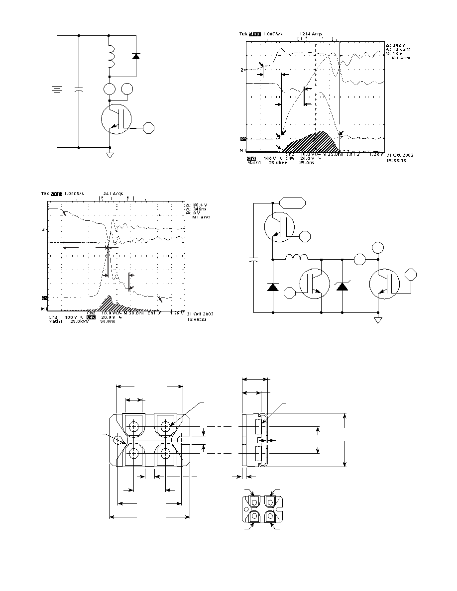
Figure 22, Turn-on Switching Waveforms and Definitions
Figure 23, Turn-off Switching Waveforms and Definitions
SOT-227 (ISOTOP
Æ
) Package Outline
31.5 (1.240)
31.7 (1.248)
Dimensions in Millimeters and (Inches)
7.8 (.307)
8.2 (.322)
30.1 (1.185)
30.3 (1.193)
38.0 (1.496)
38.2 (1.504)
14.9 (.587)
15.1 (.594)
11.8 (.463)
12.2 (.480)
8.9 (.350)
9.6 (.378)
Hex Nut M4
(4 places)
0.75 (.030)
0.85 (.033)
12.6 (.496)
12.8 (.504)
25.2 (0.992)
25.4 (1.000)
1.95 (.077)
2.14 (.084)
* Emitter
Collector
Gate
*
r = 4.0 (.157)
(2 places)
4.0 (.157)
4.2 (.165)
(2 places)
W=4.1 (.161)
W=4.3 (.169)
H=4.8 (.187)
H=4.9 (.193)
(4 places)
3.3 (.129)
3.6 (.143)
* Emitter
Emitter terminals are shorted
internally. Current handling
capability is equal for either
Source terminal.
*DRIVER SAME TYPE AS D.U.T.
I
C
V
CLAMP
100uH
V
TEST
A
A
B
D.U.T.
DRIVER*
V
CE
Figure 24, E
ON1
Test Circuit
I
C
A
D.U.T.
APT60DF60
V
CE
Figure 21, Inductive Switching Test Circuit
V
CC
T
J
= 125 C
Collector Voltage
Gate Voltage
Collector Current
90%
t
d(off)
90%
t
f
10%
0
Switching
Energy
T
J
= 125 C
10%
10%
5%
t
d(on)
90%
t
r
5 %
Switching
Energy
Collector Voltage
Collector Current
Gate Voltage
APT's products are covered by one or more of U.S.patents 4,895,810 5,045,903 5,089,434 5,182,234 5,019,522
5,262,336 6,503,786 5,256,583 4,748,103 5,283,202 5,231,474 5,434,095 5,528,058 and foreign patents. US and Foreign patents pending. All Rights Reserved.
ISOTOP
Æ
is a Registered Trademark of SGS Thomson.