
APTGF50TDU120P
A
P
T
G
F
5
0
T
D
U
120
P
≠ R
e
v 0 S
e
pt
e
m
be
r
,
2004
APT website ≠ http://www.advancedpower.com
1 - 6
Application
∑ AC Switches
∑ Switched Mode Power Supplies
∑ Uninterruptible Power Supplies
Features
∑ Non Punch Through (NPT) FAST IGBT
- Low voltage drop
- Low tail current
- Switching frequency up to 50 kHz
- Soft recovery parallel diodes
- Low diode VF
- Low leakage current
- Avalanche energy rated
- RBSOA and SCSOA rated
∑ Kelvin emitter for easy drive
∑ Very low stray inductance
-
Symmetrical design
-
Lead frames for power connections
∑ High level of integration
Benefits
∑ Outstanding performance at high frequency
operation
∑ Direct mounting to heatsink (isolated package)
∑ Low junction to case thermal resistance
∑ Solderable terminals both for power and signal for
easy PCB mounting
∑ Very low (12mm) profile
∑ Easy paralleling due to positive TC of VCEsat
∑ Each leg can be easily paralleled to achieve a dual
common source configuration of three times the
current capability
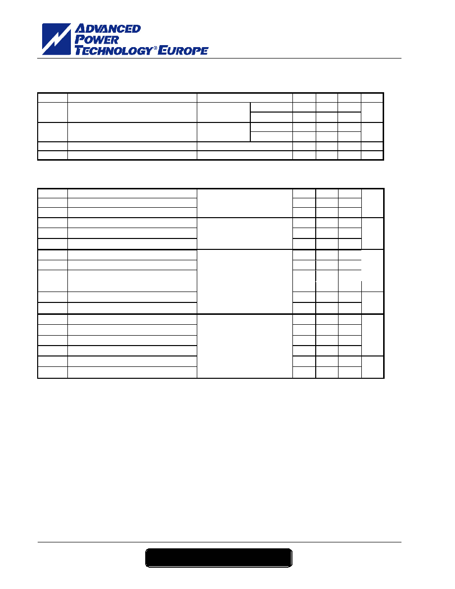
Absolute maximum ratings
These Devices are sensitive to Electrostatic Discharge. Proper Handing Procedures Should Be Followed.
E5/E6
G5
E5
E3/E4
C5
G3
C6
E6
G6
C2
E2
G2
C4
E4
G4
E1
C1
G1
E1/E2
C3
E3
E5
G5
C 5
C 3
G3
E5/E6
E3
E6
G6
C 4
C 6
E4
G4
E1
E1/E2
E3/E4
C 1
G1
G2
E2
C 2
Symbol Parameter
Max ratings
Unit
V
CES
Collector - Emitter Breakdown Voltage
1200
V
T
c
= 25∞C
75
I
C
Continuous
Collector
Current
T
c
= 80∞C
50
I
CM
Pulsed Collector Current
T
c
= 25∞C
150
A
V
GE
Gate ≠ Emitter Voltage
±20
V
P
D
Maximum Power Dissipation
T
c
= 25∞C
312 W
RBSOA Reverse Bias Safe Operating Area
T
j
= 150∞C
150A @ 1200V
V
CES
= 1200V
I
C
= 50A @ Tc = 80∞C
Triple dual Common Source
NPT IGBT Power Module
APTGF50TDU120P
A
P
T
G
F
5
0
T
D
U
120
P
≠ R
e
v 0 S
e
pt
e
m
be
r
,
2004
APT website ≠ http://www.advancedpower.com
2 - 6
All ratings @ T
j
= 25∞C unless otherwise specified
Electrical Characteristics
Symbol Characteristic
Test
Conditions
Min Typ Max Unit
BV
CES
Collector - Emitter Breakdown Voltage
V
GE
= 0V, I
C
= 500 µA
1200
V
T
j
= 25∞C
500
I
CES
Zero Gate Voltage Collector Current
V
GE
= 0V
V
CE
= 1200V
T
j
= 125∞C
2500
µA
T
j
= 25∞C
3.2
3.7
V
CE(on)
Collector Emitter on Voltage
V
GE
=15V
I
C
= 50A
T
j
= 125∞C
4.0
V
V
GE(th)
Gate
Threshold
Voltage
V
GE
= V
CE
, I
C
= 1 mA
4.5
6.5
V
I
GES
Gate ≠ Emitter Leakage Current
V
GE
= ±20 V, V
CE
= 0V
100
nA
Dynamic Characteristics
Symbol Characteristic
Test
Conditions
Min Typ Max Unit
C
ies
Input
Capacitance
3450
C
oes
Output
Capacitance
330
C
res
Reverse Transfer Capacitance
V
GE
= 0V
V
CE
= 25V
f = 1MHz
220
pF
Q
g
Total gate Charge
330
Q
ge
Gate ≠ Emitter Charge
35
Q
gc
Gate ≠ Collector Charge
V
GS
= 15V
V
Bus
= 600V
I
C
= 50A
200
nC
T
d(on)
Turn-on Delay Time
35
T
r
Rise Time
65
T
d(off)
Turn-off Delay Time
320
T
f
Fall Time
30
ns
E
on
Turn-on Switching Energy
5.4
E
off
Turn-off Switching Energy
Inductive Switching (25∞C)
V
GE
= 15V
V
Bus
= 600V
I
C
= 50A
R
G
= 5
2.3
mJ
T
d(on)
Turn-on
Delay
Time
35
T
r
Rise Time
65
T
d(off)
Turn-off Delay Time
360
T
f
Fall Time
40
ns
E
on
Turn-on Switching Energy
6.9
E
off
Turn-off Switching Energy
Inductive Switching (125∞C)
V
GE
= 15V
V
Bus
= 600V
I
C
= 50A
R
G
= 5
3.05
mJ
E
on
includes diode reverse recovery
In accordance with JEDEC standard JESD24-1
APTGF50TDU120P
A
P
T
G
F
5
0
T
D
U
120
P
≠ R
e
v 0 S
e
pt
e
m
be
r
,
2004
APT website ≠ http://www.advancedpower.com
3 - 6
Reverse diode ratings and characteristics
Symbol Characteristic
Test
Conditions
Min Typ Max Unit
V
RRM
Maximum Peak Repetitive Reverse Voltage
1200
V
T
j
= 25∞C
250
I
RM
Maximum Reverse Leakage Current
V
R
=1200V
T
j
= 125∞C
500
µA
I
F(A V)
Maximum Average Forward Current
50% duty cycle
Tc = 70∞C
60
A
I
F
= 60A
2
2.5
I
F
= 120A
2.3
V
F
Diode Forward Voltage
I
F
= 60A
T
j
= 125∞C
1.8
V
T
j
= 25∞C
400
t
rr
Reverse Recovery Time
T
j
= 125∞C
470
ns
T
j
= 25∞C
1200
Q
rr
Reverse Recovery Charge
I
F
= 60A
V
R
= 800V
di/dt =200A/µs
T
j
= 125∞C
4000
nC
Thermal and package characteristics
Symbol Characteristic
Min Typ Max Unit
IGBT 0.4
R
thJC
Junction
to
Case
Diode
0.9
∞C/W
V
ISOL
RMS Isolation Voltage, any terminal to case t =1 min, I isol<1mA, 50/60Hz
2500 V
T
J
Operating junction temperature range
-40
150
T
STG
Storage Temperature Range
-40
125
T
C
Operating Case Temperature
-40
100
∞C
Torque Mounting torque
To heatsink
M6
3
5
N.m
Wt Package
Weight
250 g
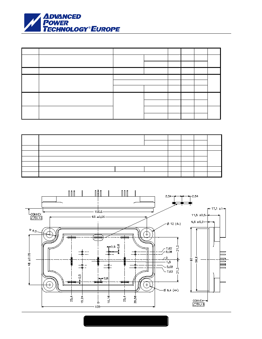
Package outline
5 places (3:1)
APTGF50TDU120P
A
P
T
G
F
5
0
T
D
U
120
P
≠ R
e
v 0 S
e
pt
e
m
be
r
,
2004
APT website ≠ http://www.advancedpower.com
4 - 6
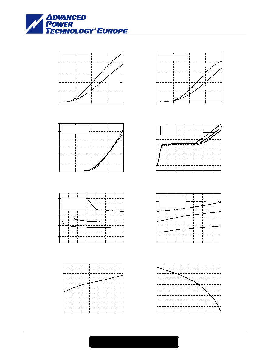
Typical Performance Curve
Output characteristics (V
GE
=15V)
T
J
=25∞C
T
J
=125∞C
0
40
80
120
160
200
0
2
4
6
8
I
c
, C
o
lle
c
t
o
r
C
u
r
r
e
n
t
(
A
)
V
CE
, Collector to Emitter Voltage (V)
250µs Pulse Test
< 0.5% Duty cycle
Output Characteristics (V
GE
=10V)
T
J
=25∞C
T
J
=125∞C
0
10
20
30
40
50
0
1
2
3
4
Ic
, Co
ll
e
c
t
o
r
Cu
r
r
e
n
t
(
A
)
V
CE
, Collector to Emitter Voltage (V)
250µs Pulse Test
< 0.5% Duty cycle
Transfer Characteristics
T
J
=25∞C
T
J
=125∞C
0
50
100
150
200
250
300
0
4
8
12
16
V
GE
, Gate to Emitter Voltage (V)
Ic
,
Co
lle
c
t
o
r
Cu
r
r
e
n
t
(
A
)
250µs Pulse Test
< 0.5% Duty cycle
Gate Charge
V
CE
=240V
V
CE
=600V
V
CE
=960V
0
2
4
6
8
10
12
14
16
18
0
50
100
150
200
250
300
350
Gate Charge (nC)
V
GE
,
G
ate
to
E
m
i
t
t
e
r
V
o
l
t
ag
e
(V
)
I
C
= 50A
T
J
= 25∞C
Ic=100A
Ic=50A
Ic=25A
0
1
2
3
4
5
6
7
8
9
9
10
11
12
13
14
15
16
V
GE
, Gate to Emitter Voltage (V)
On state Voltage vs Gate to Emitter Volt.
V
CE
,
C
o
l
l
e
c
t
o
r
to
E
m
i
t
ter
V
o
l
tag
e (V
)
T
J
= 25∞C
250µs Pulse Test
< 0.5% Duty cycle
Ic=100A
Ic=50A
Ic=25A
0
1
2
3
4
5
6
-50
-25
0
25
50
75
100
125
T
J
, Junction Temperature (∞C)
V
CE
,
C
o
l
l
ect
o
r
to
E
m
i
t
te
r
V
o
l
t
a
g
e (V
) On state Voltage vs Junction Temperature
250µs Pulse Test
< 0.5% Duty cycle
V
GE
= 15V
0.70
0.75
0.80
0.85
0.90
0.95
1.00
1.05
1.10
1.15
1.20
-50
-25
0
25
50
75
100 125
T
J
, Junction Temperature (∞C)
C
o
l
l
e
cto
r
to
E
m
i
t
t
e
r
B
r
e
akd
o
w
n
V
o
l
t
ag
e
(
N
orm
a
l
i
z
e
d)
Breakdown Voltage vs Junction Temp.
0
10
20
30
40
50
60
70
80
90
-50 -25
0
25
50
75
100 125 150
T
C
, Case Temperature (∞C)
I
c
,
DC
Co
ll
e
c
t
o
r
Cu
r
r
e
n
t
(
A
)
DC Collector Current vs Case Temperature
APTGF50TDU120P
A
P
T
G
F
5
0
T
D
U
120
P
≠ R
e
v 0 S
e
pt
e
m
be
r
,
2004
APT website ≠ http://www.advancedpower.com
5 - 6
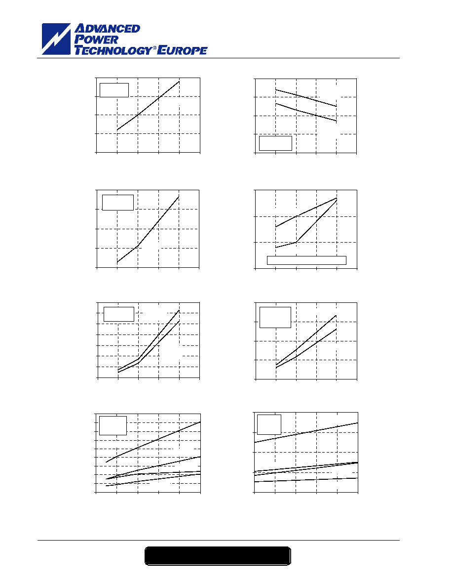
V
GE
= 15V
25
30
35
40
45
0
25
50
75
100
125
I
CE
, Collector to Emitter Current (A)
t
d
(
on)
,
Turn-
O
n
D
e
l
a
y
Ti
m
e
(
n
s
)
Turn-On Delay Time vs Collector Current
V
CE
= 600V
R
G
= 5
V
GE
=15V,
T
J
=25∞C
V
GE
=15V,
T
J
=125∞C
200
250
300
350
400
0
25
50
75
100
125
I
CE
, Collector to Emitter Current (A)
Turn-Off Delay Time vs Collector Current
t
d
(
o
f
f
)
,
Turn-
O
f
f
D
e
l
a
y
Ti
m
e
(
n
s
)
V
CE
= 600V
R
G
= 5
V
GE
=15V
20
60
100
140
180
0
25
50
75
100
125
I
CE
, Collector to Emitter Current (A)
t
r
,
R
i
se T
i
m
e
(n
s
)
Current Rise Time vs Collector Current
V
CE
= 600V
R
G
= 5
T
J
= 25∞C
T
J
= 125∞C
20
30
40
50
0
25
50
75
100
125
I
CE
, Collector to Emitter Current (A)
t
f
,
F
a
ll T
i
m
e
(
n
s
)
Current Fall Time vs Collector Current
V
CE
= 600V, V
GE
= 15V, R
G
= 5
T
J
=25∞C,
V
GE
=15V
T
J
=125∞C,
V
GE
=15V
0
4
8
12
16
20
24
28
0
25
50
75
100
125
I
CE
, Collector to Emitter Current (A)
Turn-On Energy Loss vs Collector Current
E
o
n,
Tur
n-
O
n
E
n
e
r
gy
Los
s
(
m
J
)
V
CE
= 600V
R
G
= 5
T
J
= 25∞C
T
J
= 125∞C
0
2
4
6
8
0
25
50
75
100
125
I
CE
, Collector to Emitter Current (A)
E
o
f
f
,
Tu
rn-
o
f
f
E
n
e
r
gy
Los
s
(
m
J
)
Turn-Off Energy Loss vs Collector Current
V
CE
= 600V
V
GE
= 15V
R
G
= 5
Eon, 50A
Eoff, 50A
Eon, 25A
Eoff, 25A
0
2
4
6
8
10
12
14
16
18
0
10
20
30
40
50
Gate Resistance (Ohms)
S
w
i
t
c
h
i
n
g
E
n
er
g
y
L
o
sse
s (m
J)
Switching Energy Losses vs Gate Resistance
V
CE
= 600V
V
GE
= 15V
T
J
= 125∞C
Eon, 50A
Eoff, 50A
Eon, 25A
Eoff, 25A
0
2
4
6
8
0
25
50
75
100
125
T
J
, Junction Temperature (∞C)
S
w
i
t
c
h
i
ng E
n
e
r
gy
Los
s
e
s
(
m
J
)
Switching Energy Losses vs Junction Temp.
V
CE
= 600V
V
GE
= 15V
R
G
= 5
APTGF50TDU120P
A
P
T
G
F
5
0
T
D
U
120
P
≠ R
e
v 0 S
e
pt
e
m
be
r
,
2004
APT website ≠ http://www.advancedpower.com
6 - 6
Cies
Cres
Coes
100
1000
10000
0
10
20
30
40
50
C
,
C
a
p
aci
t
a
n
c
e
(
p
F
)
Capacitance vs Collector to Emitter Voltage
V
CE
, Collector to Emitter Voltage (V)
0
20
40
60
80
100
120
140
160
0
400
800
1200
I
C
, C
o
lle
c
t
o
r
C
u
r
r
e
n
t
(
A
)
Minimum Switching Safe Operating Area
V
CE
, Collector to Emitter Voltage (V)
0.9
0.7
0.5
0.3
0.1
0.05
Single Pulse
0
0.05
0.1
0.15
0.2
0.25
0.3
0.35
0.4
0.45
0.00001
0.0001
0.001
0.01
0.1
1
Rectangular Pulse Duration (Seconds)
Th
e
r
m
a
l
I
m
pe
da
nc
e
(
∞
C
/
W
)
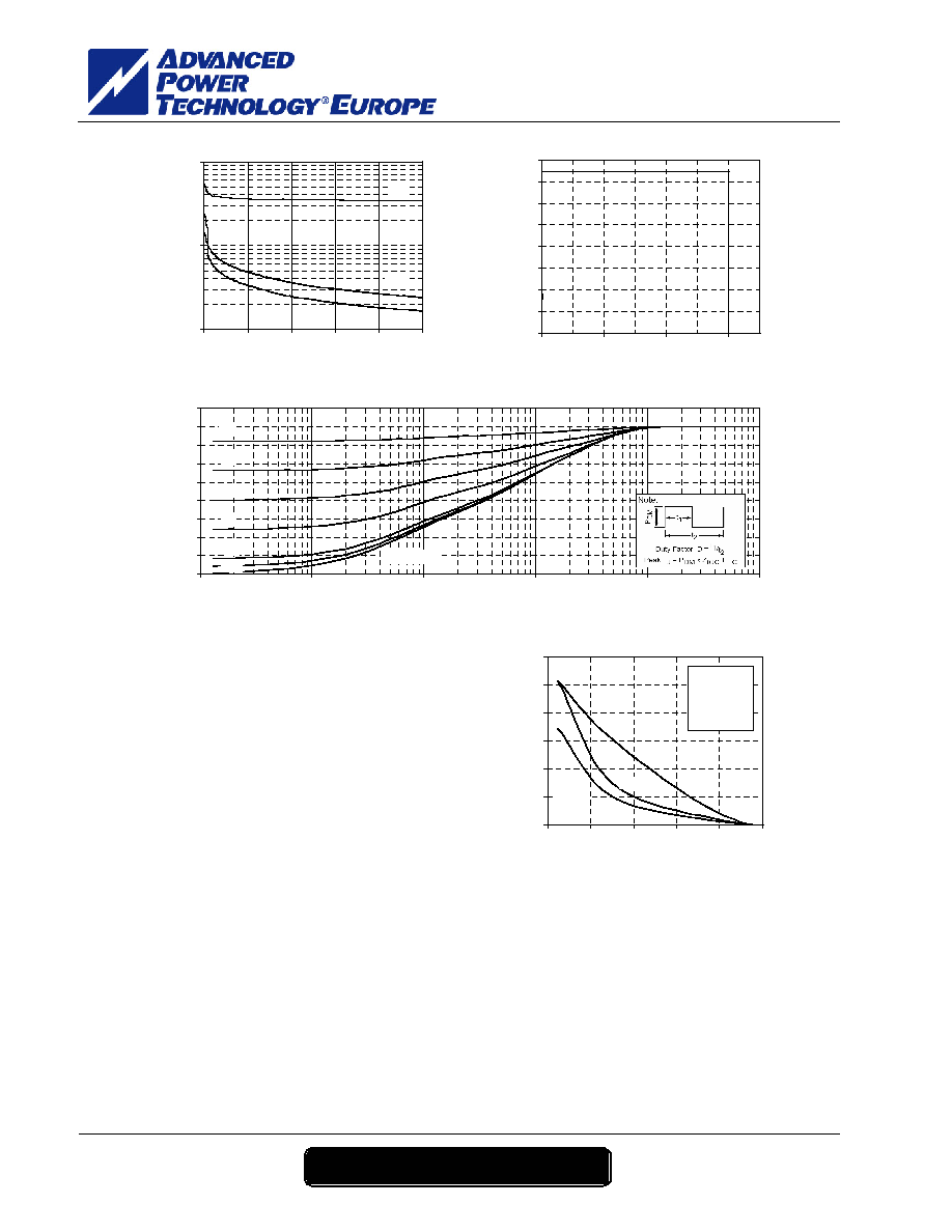
Maximum Effective Transient Thermal Impedance, Junction to Case vs Pulse Duration
Hard
switching
ZCS
ZVS
0
20
40
60
80
100
120
10
20
30
40
50
60
I
C
, Collector Current (A)
Operating Frequency vs Collector Current
Fm
a
x
,
O
p
e
r
a
t
i
n
g F
r
e
q
ue
n
c
y
(
k
H
z
)
V
CE
= 600V
D = 50%
R
G
= 5
T
J
= 125∞C
T
C
= 75∞C
APT reserves the right to change, without notice, the specifications and information contained herein
APT's products are covered by one or more of U.S patents 4,895,810 5,045,903 5,089,434 5,182,234 5,019,522
5,262,336 6,503,786 5,256,583 4,748,103 5,283,202 5,231,474 5,434,095 5,528,058 and foreign patents. U.S and Foreign patents pending. All Rights Reserved.