Äîêóìåíòàöèÿ è îïèñàíèÿ www.docs.chipfind.ru
APTM120UM70F-AlN
A
P
T
M
120U
M
70F
A
l
N
R
e
v 0 J
u
l
y, 2004
APT website http://www.advancedpower.com
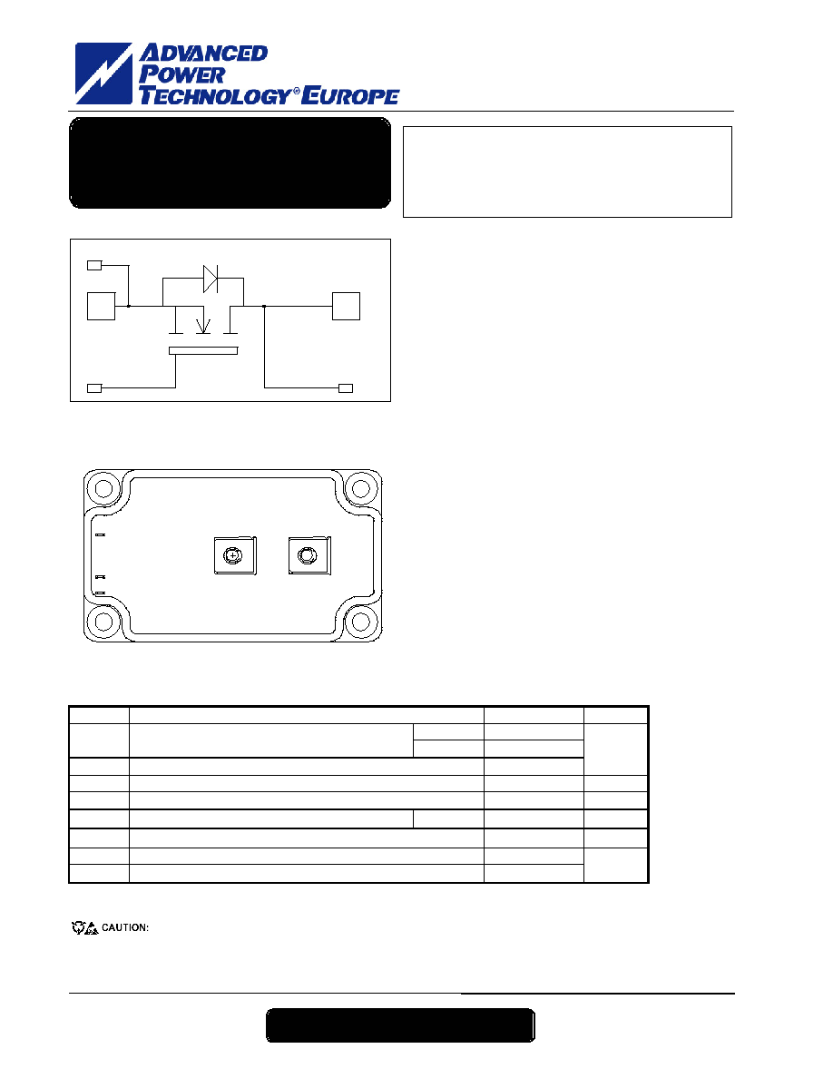
1 6
D
G
DK
S
SK
D
S
DK
G
SK
Absolute maximum ratings
These Devices are sensitive to Electrostatic Discharge. Proper Handing Procedures Should Be Followed.
Symbol Parameter
Max ratings
Unit
V
DSS
Drain - Source Breakdown Voltage
1200
V
T
c
= 25°C
171
I
D
Continuous
Drain
Current
T
c
= 80°C
126
I
DM
Pulsed Drain current
684
A
V
GS
Gate - Source Voltage
±30
V
R
DSon
Drain - Source ON Resistance
70
m
P
D
Maximum Power Dissipation
T
c
= 25°C
5000
W
I
AR
Avalanche current (repetitive and non repetitive)
24
A
E
AR
Repetitive Avalanche Energy
50
E
AS
Single Pulse Avalanche Energy
3200
mJ
V
DSS
= 1200V
R
DSon
= 70m
max @ Tj = 25°C
I
D
= 171A @ Tc = 25°C
Application
· Welding converters
· Switched Mode Power Supplies
· Uninterruptible Power Supplies
· Motor control
Features
· Power MOS 7
®
FREDFETs
- Low R
DSon
- Low input and Miller capacitance
- Low gate charge
- Fast intrinsic reverse diode
- Avalanche energy rated
- Very rugged
· Kelvin source for easy drive
· Very low stray inductance
- Symmetrical design
- M5 power connectors
· High level of integration
· AlN substrate for improved thermal performance
Benefits
· Outstanding performance at high frequency operation
· Direct mounting to heatsink (isolated package)
· Low junction to case thermal resistance
· Low profile
Single switch
MOSFET Power Module
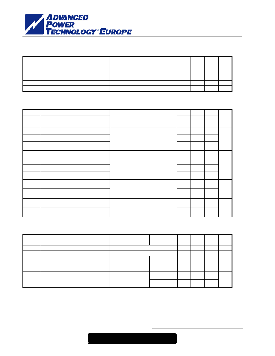
APTM120UM70F-AlN
A
P
T
M
120U
M
70F
A
l
N
R
e
v 0 J
u
l
y, 2004
APT website http://www.advancedpower.com
2 6
All ratings @ T
j
= 25°C unless otherwise specified
Electrical Characteristics
Symbol Characteristic
Test
Conditions
Min Typ Max Unit
BV
DSS
Drain - Source Breakdown Voltage V
GS
= 0V, I
D
= 1.5mA
1200
V
V
GS
= 0V,V
DS
= 1200V
T
j
= 25°C
1.5
I
DSS
Zero Gate Voltage Drain Current
V
GS
= 0V,V
DS
= 1000V
T
j
= 125°C
6
mA
R
DS(on)
Drain Source on Resistance
V
GS
= 10V, I
D
= 85.5A
70
m
V
GS(th)
Gate
Threshold
Voltage
V
GS
= V
DS
, I
D
=
30mA
3 5 V
I
GSS
Gate Source Leakage Current
V
GS
= ±30
V, V
DS
= 0V
±600
nA
Dynamic Characteristics
Symbol Characteristic
Test
Conditions
Min Typ Max Unit
C
iss
Input
Capacitance
43.5
C
oss
Output
Capacitance
6.6
C
rss
Reverse Transfer Capacitance
V
GS
= 0V
V
DS
= 25V
f = 1MHz
1.2
nF
Q
g
Total gate Charge
1650
Q
gs
Gate Source Charge
192
Q
gd
Gate Drain Charge
V
GS
= 10V
V
Bus
= 600V
I
D
= 171A
1074
nC
T
d(on)
Turn-on
Delay
Time
20
T
r
Rise Time
17
T
d(off)
Turn-off Delay Time
245
T
f
Fall Time
Inductive switching @ 125°C
V
GS
= 15V
V
Bus
= 800V
I
D
= 171A
R
G
=0.8
62
ns
E
on
Turn-on Switching Energy
7.6
E
off
Turn-off Switching Energy
Inductive switching @ 25°C
V
GS
= 15V, V
Bus
= 800V
I
D
= 171A,
R
G
= 0.8
6.9
mJ
E
on
Turn-on Switching Energy
13.8
E
off
Turn-off Switching Energy
Inductive switching @ 125°C
V
GS
= 15V, V
Bus
= 800V
I
D
= 171A,
R
G
= 0.8
8.5
mJ
Source - Drain diode ratings and characteristics
Symbol Characteristic
Test
Conditions
Min Typ Max Unit
Tc = 25°C
171
I
S
Continuous Source current
(Body diode)
Tc = 80°C
126
A
V
SD
Diode Forward Voltage
V
GS
= 0V, I
S
= - 171A
1.3
V
dv/dt
Peak Diode Recovery
18
V/ns
T
j
= 25°C
375
t
rr
Reverse Recovery Time
I
S
= - 171A
V
R
= 600V
di
S
/dt = 600A/µs
T
j
= 125°C
860
ns
T
j
= 25°C
12
Q
rr
Reverse Recovery Charge
I
S
= - 171A
V
R
= 600V
di
S
/dt = 600A/µs
T
j
= 125°C
54
µC
E
on
includes diode reverse recovery.
In accordance with JEDEC standard JESD24-1.
dv/dt numbers reflect the limitations of the circuit rather than the device itself.
I
S
- 171A di/dt 700A/µs V
R
V
DSS
T
j
150°C
APTM120UM70F-AlN
A
P
T
M
120U
M
70F
A
l
N
R
e
v 0 J
u
l
y, 2004
APT website http://www.advancedpower.com
3 6
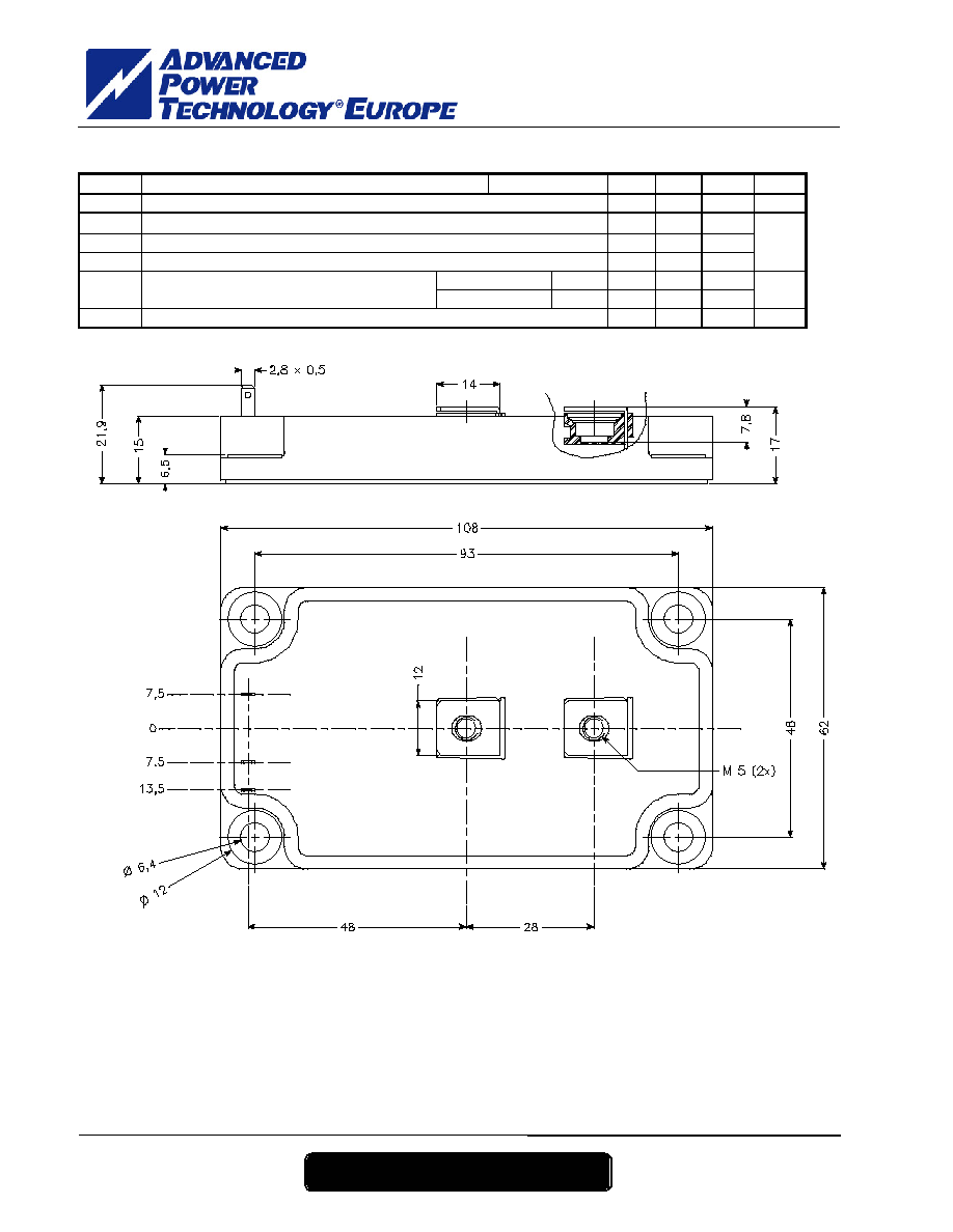
Thermal and package characteristics
Symbol Characteristic
Min Typ Max Unit
R
thJC
Junction
to
Case
Transistor
0.025 °C/W
V
ISOL
RMS Isolation Voltage, any terminal to case t =1 min, I isol<1mA, 50/60Hz
2500 V
T
J
Operating junction temperature range
-40 150
T
STG
Storage Temperature Range
-40
125
T
C
Operating Case Temperature
-40
100
°C
To heatsink
M6
3
5
Torque Mounting
torque
For terminals
M5
2
3.5
N.m
Wt Package
Weight
280 g
Package outline
APTM120UM70F-AlN
A
P
T
M
120U
M
70F
A
l
N
R
e
v 0 J
u
l
y, 2004
APT website http://www.advancedpower.com
4 6
Typical Performance Curve
0.9
0.7
0.5
0.3
0.1
0.05
Single Pulse
0
0.005
0.01
0.015
0.02
0.025
0.03
0.00001
0.0001
0.001
0.01
0.1
1
10
rectangular Pulse Duration (Seconds)
T
h
e
r
m
a
l
I
m
pe
da
nc
e
(
°
C
/
W
)
Maximum Effective Transient Thermal Impedance, Junction to Case vs Pulse Duration
4.5V
5V
5.5V
6V
7V
0
60
120
180
240
300
360
420
0
5
10
15
20
25
30
V
DS
, Drain to Source Voltage (V)
I
D
,
Dr
a
i
n
Cu
r
r
e
n
t
(
A
)
V
GS
=15, 10V
Low Voltage Output Characteristics
Transfert Characteristics
T
J
=-55°C
T
J
=25°C
T
J
=125°C
0
60
120
180
240
300
360
420
480
0
1
2
3
4
5
6
7
V
GS
, Gate to Source Voltage (V)
I
D
,
Dr
a
i
n
Cu
r
r
e
n
t
(
A
)
V
DS
> I
D
(on)xR
DS
(on)MAX
250µs pulse test @ < 0.5 duty cycle
R
DS(on)
vs Drain Current
V
GS
=10V
V
GS
=20V
0.8
0.9
1
1.1
1.2
1.3
1.4
0
60
120
180
240
300
360
I
D
, Drain Current (A)
R
DS
(
o
n
)
D
r
ai
n
t
o
S
o
u
r
ce O
N
R
e
si
st
an
ce
Normalized to
V
GS
=10V @ 85.5A
0
45
90
135
180
25
50
75
100
125
150
T
C
, Case Temperature (°C)
I
D
,
DC
D
r
a
i
n
Cu
r
r
e
n
t
(
A
)
DC Drain Current vs Case Temperature

APTM120UM70F-AlN
A
P
T
M
120U
M
70F
A
l
N
R
e
v 0 J
u
l
y, 2004
APT website http://www.advancedpower.com
5 6
0.85
0.90
0.95
1.00
1.05
1.10
1.15
-50 -25
0
25 50 75 100 125 150
T
J
, Junction Temperature (°C)
BV
DS
S
,
D
r
ai
n
t
o
S
o
u
r
ce
B
r
eak
d
o
w
n
V
o
l
t
ag
e (
N
o
r
m
a
l
i
z
e
d
)
Breakdown Voltage vs Temperature
ON resistance vs Temperature
0.0
0.5
1.0
1.5
2.0
2.5
-50 -25
0
25 50 75 100 125 150
T
J
, Junction Temperature (°C)
R
DS
(
o
n
)
,
D
r
a
i
n
t
o
S
o
u
r
ce O
N
r
esi
st
an
ce
(
N
or
m
a
l
i
z
e
d)
V
GS
=10V
I
D
=85.5A
Threshold Voltage vs Temperature
0.6
0.7
0.8
0.9
1.0
1.1
1.2
-50 -25
0
25 50 75 100 125 150
T
C
, Case Temperature (°C)
V
GS
(
T
H
)
,
Th
r
e
s
hol
d
V
o
l
t
a
g
e
(N
o
r
ma
l
i
z
e
d
)
Maximum Safe Operating Area
10ms
1ms
100µs
1
10
100
1000
1
10
100
1000
V
DS
, Drain to Source Voltage (V)
I
D
,
Dr
a
i
n
Cu
r
r
e
n
t
(
A
)
limited by R
DS
on
Single pulse
T
J
=150°C
1200
Ciss
Crss
Coss
1000
10000
100000
0
10
20
30
40
50
V
DS
, Drain to Source Voltage (V)
C
,
C
a
p
aci
t
a
n
ce (
p
F
)
Capacitance vs Drain to Source Voltage
V
DS
=240V
V
DS
=600V
V
DS
=960V
0
2
4
6
8
10
12
14
0
420
840
1260
1680
2100
Gate Charge (nC)
V
GS
,
G
a
t
e
t
o
S
o
u
r
ce V
o
l
t
ag
e
(
V
)
Gate Charge vs Gate to Source Voltage
I
D
=171A
T
J
=25°C

APTM120UM70F-AlN
A
P
T
M
120U
M
70F
A
l
N
R
e
v 0 J
u
l
y, 2004
APT website http://www.advancedpower.com
6 6
Delay Times vs Current
t
d(on)
t
d(off)
0
50
100
150
200
250
300
60
90
120 150 180 210 240 270
I
D
, Drain Current (A)
t
d(o
n
)
a
nd t
d(
off
)
(n
s
)
V
DS
=800V
R
G
=0.8
T
J
=125°C
L=100µH
Rise and Fall times vs Current
t
r
t
f
0
20
40
60
80
100
60
90
120 150 180 210 240 270
I
D
, Drain Current (A)
t
r
an
d
t
f
(n
s
)
V
DS
=800V
R
G
=0.8
T
J
=125°C
L=100µH
Switching Energy vs Current
E
on
E
off
0
4
8
12
16
20
24
60
90 120 150 180 210 240 270
I
D
, Drain Current (A)
Sw
i
t
c
h
i
n
g
Ene
r
gy
(
m
J
)
V
DS
=800V
R
G
=0.8
T
J
=125°C
L=100µH
E
on
E
off
6
12
18
24
30
36
0
1
2
3
4
5
6
Gate Resistance (Ohms)
Sw
i
t
c
h
i
n
g
Ene
r
gy
(
m
J
)
Switching Energy vs Gate Resistance
V
DS
=800V
I
D
=171A
T
J
=125°C
L=100µH
Hard
switching
ZCS
ZVS
0
25
50
75
100
125
150
175
40
60
80
100
120
140
160
I
D
, Drain Current (A)
F
r
eq
u
e
n
cy (
k
H
z
)
Operating Frequency vs Drain Current
V
DS
=800V
D=50%
R
G
=0.8
T
J
=125°C
T
C
=75°C
T
J
=25°C
T
J
=150°C
1
10
100
1000
0.2 0.4 0.6 0.8
1
1.2 1.4 1.6 1.8
V
SD