 | –≠–ª–µ–∫—Ç—Ä–æ–Ω–Ω—ã–π –∫–æ–º–ø–æ–Ω–µ–Ω—Ç: ARF450 | –°–∫–∞—á–∞—Ç—å:  PDF PDF  ZIP ZIP |
050-4910
Rev
C
12-2000
MAXIMUM RATINGS
All Ratings: T
C
= 25∞C unless otherwise specified.
STATIC ELECTRICAL CHARACTERISTICS
Symbol
BV
DSS
V
DS
(ON)
I
DSS
I
GSS
g
fs
g
fs1
/
g
fs2
V
GS
(TH)
V
GS
(TH)
Characteristic / Test Conditions
Drain-Source Breakdown Voltage (V
GS
= 0V, I
D
= 250 µA)
On State Drain Voltage
1
(I
D
(ON)
= 5.5A, V
GS
= 10V)
Zero Gate Voltage Drain Current (V
DS
= V
DSS
, V
GS
= 0V)
Zero Gate Voltage Drain Current (V
DS
= 0.8 V
DSS
, V
GS
= 0V, T
C
= 125∞C)
Gate-Source Leakage Current (V
GS
= ±30V, V
DS
= 0V)
Forward Transconductance (V
DS
= 25V, I
D
= 5.5A)
Forward Transconductance Ratio (V
DS
= 25V, I
D
= 5.5A)
Gate Threshold Voltage (V
DS
= V
GS
, I
D
= 50mA)
Delta Gate Threshold Voltage (V
DS
= V
GS
, I
D
= 50mA)
MIN
TYP
MAX
500
5
25
250
±100
35.8
0.9
1.1
3
5
0.1
UNIT
Volts
µA
nA
mhos
Volts
Symbol
V
DSS
V
DGO
I
D
V
GS
P
D
T
J
,T
STG
T
L
Parameter
Drain-Source Voltage
Drain-Gate Voltage
Continuous Drain Current @ T
C
= 25∞C
Gate-Source Voltage
Total Device Dissipation @ T
C
= 25∞C
Operating and Storage Junction Temperature Range
Lead Temperature: 0.063" from Case for 10 Sec.
ARF450
450
450
11
±30
650
-55 to 200
300
UNIT
Volts
Amps
Volts
Watts
∞C
RF POWER MOSFET
N- CHANNEL ENHANCEMENT MODE
150V 500W 120MHz
The ARF450 is a matched pair of RF power transistors in a common source configuration. It is designed for push-pull
or parallel operation in scientific, commercial, medical and industrial RF power amplifier applications up to 120 MHz.
Specified 150 Volt, 81.36 MHz Characteristics:
Output Power = 500 Watts.
Gain = 13dB (Class C)
Efficiency = 75%
High Performance Push-Pull RF Package.
Very High Breakdown for Improved Ruggedness.
Low Thermal Resistance.
Nitride Passivated Die for Improved Reliability.
ARF450
Common Source
Push-Pull Pair
ARF450
BeO
11405
CAUTION: These Devices are Sensitive to Electrostatic Discharge. Proper Handling Procedures Should Be Followed.
USA:
405 S.W. Columbia Street Bend, Oregon 97702-1035
Phone: (541) 382-8028 FAX: (541) 388 -0364
EUROPE: Chemin de Magret
F-33700 Merignac - France
Phone: (33) 5 57 92 15 15 FAX: (33) 5 56 47 9761
APT Website - http://www.advancedpower.com
THERMAL CHARACTERISTICS
Symbol
R
JC
R
CS
Characteristic (per package unless otherwise noted)
Junction to Case (per section)
Case to Sink
(Use High Efficiency Thermal Joint Compound and Planar Heat Sink Surface.)
MIN
TYP
MAX
0.54
0.1
UNIT
∞C/W
050-4910
Rev
C
12-2000
DYNAMIC CHARACTERISTICS (per section)
ARF450
Symbol
C
iss
C
oss
C
rss
t
d(on)
t
r
t
d(off)
t
f
Characteristic
Input Capacitance
Output Capacitance
Reverse Transfer Capacitance
Turn-on Delay Time
Rise Time
Turn-off Delay Time
Fall Time
Test Conditions
V
GS
= 0V
V
DS
= 150V
f = 1 MHz
V
GS
= 15V
V
DD
= 0.5 V
DSS
I
D
= I
D[Cont.]
@ 25∞C
R
G
= 1.6
MIN
TYP
MAX
980
1200
87
120
25
40
5
10
3.0
7
15
25
3
7
UNIT
pF
ns
FUNCTIONAL CHARACTERISTICS
(Push-Pull Configuration)
Symbol
G
PS
Test Conditions
f = 81.36 MHz
V
GS
= 0V V
DD
= 150V
P
out
= 500W
No Degradation in Output Power
Characteristic
Common Source Amplifier Power Gain
Drain Efficiency
Electrical Ruggedness VSWR 10:1
MIN
TYP
MAX
12
13
70
75
UNIT
dB
%
1
Pulse Test: Pulse width < 380 µS, Duty Cycle < 2%.
APT Reserves the right to change, without notice, the specifications and information contained herein.
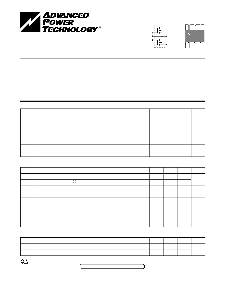
GAIN (dB)
FREQUENCY (MHz)
Figure 1, Typical Gain vs Frequency
30
25
20
15
10
5
0
30
45
60
75
90
105
120
Class C
V
DD
= 150V
P
out
= 150W
16
12
8
4
0
0
2
4
6
8
CAPACITANCE
(pf)
V
DS
, DRAIN-TO-SOURCE VOLTAGE (VOLTS)
Figure 2, Typical Capacitance vs. Drain-to-Source Voltage
3000
1000
500
100
50
10
1
5
10
50
150
V
GS
, GATE-TO-SOURCE VOLTAGE (VOLTS)
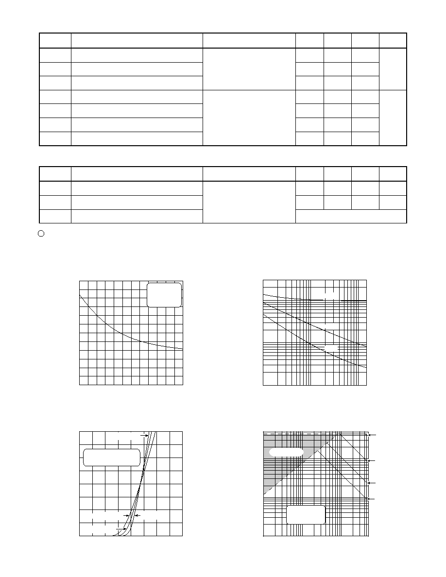
Figure 3, Typical Transfer Characteristics
I
D
, DRAIN CURRENT (AMPERES)
VDS> ID (ON) x RDS (ON)MAX.
250µSEC. PULSE TEST
@ <0.5 % DUTY CYCLE
TJ = -55∞C
TJ = -55∞C
TJ = +125∞C
TJ = +25∞C
Ciss
Coss
Crss
1
5
10
50 100
500
I
D
,
DRAIN
CURRENT
(
AMPERES)
V
DS
, DRAIN-TO-SOURCE VOLTAGE (VOLTS)
Figure 4, Typical Maximum Safe Operating Area
TC =+25∞C
TJ =+200∞C
SINGLE PULSE
OPERATION HERE
LIMITED BY RDS (ON)
Per each transistor side unless otherwise specified.
50
10
5
1
0.1
1ms
10ms
100ms
0.5
100us

050-4910
Rev
C
12-2000
G
PS
, COMMON SOURCE AMPLIFIER GAIN
(dB)
P
OUT
, POWER OUT (WATTS)
Figure 8, Typical Common Source Amplifier Gain vs Power Out
14
12
10
8
6
0
150
300
450
600
T
C
, CASE TEMPERATURE (∞C)
Figure 5, Typical Threshold Voltage vs Temperature
1.2
1.1
1.0
0.9
0.8
0.7
0.6
-50 -25
0
25
50
75 100 125 150
600
450
300
150
0
0
6
12
18
24
30
25
20
15
10
5
0
1
5
10
15
20
25
30
P
IN
, POWER IN (WATTS)
Figure 7, Typical Power Out vs Power In
P
OUT
, POWER OUT (WATTS)
V
DS
, DRAIN-TO-SOURCE VOLTAGE (VOLTS)
Figure 6, Typical Output Characteristics
I
D
, DRAIN CURRENT (AMPERES)
V
GS(th)
, THRESHOLD VOLTAGE
(NORMALIZED)
ARF450
5.5V
4.5V
5V
6V
VGS=8, 10 & 15V
V
GS
= 0
V
DD
= 150V
f = 81.36 MHz
Push-Pull
V
GS
= 0
V
DD
= 150V
f = 81.36 MHz
Push-Pull
6.5V
Freq. (MHz)
Z
in
-
gate shunted by 25
Z
OL
-
conjugate of optimum load impedance for 150W at 150V
Z
in
(
)
Z
OL
(
)
2.0
13.5
27.0
40.0
65.0
80.0
100.0
93.0 - j 10
63.0 - j 43
32.0 - j 43
17.5 - j 34
7.7 - j 22
5.1 - j 16
3.4 - j 12
23.00 - j 7.0
4.30 - j 9.1
1.00 - j 4.2
0.42 - j 1.7
0.35
+
j 1.1
0.56
+
j 2.5
0.90
+
j 3.8
Table 1 - Typical Class C Large Signal Input-Output Impedance (per section)
Z
JC
,
THERMAL
IMPEDANCE
(∞C/W)
10
-5
10
-4
10
-3
10
-2
10
-1
1.0
10
RECTANGULAR PULSE DURATION (SECONDS)
Figure 9, Typical Maximum Effective Transient Thermal Impedance, Junction-To-Case vs Pulse Duration
Note:
Duty Factor D =
t1/t
2
Peak TJ = PDM x Z
JC + TC
t1
t2
P
DM
0.1
SINGLE PULSE
0.02
0.05
0.2
D=0.5
0.01
0.6
0.1
.01
.005
.001
.05

050-4910
Rev
C
12-2000
USA:
405 S.W. Columbia Street Bend, Oregon 97702-1035
Phone: (541) 382-8028 FAX: (541) 388 -0364
EUROPE: Chemin de Magret
F-33700 Merignac - France
Phone: (33) 5 57 92 15 15 FAX: (33) 5 56 47 9761
ARF450
30 MHz Linear Test Circuit
81.36 MHz Test Circuit
J1
T1
R1
6.8K
J2
80 V
+
+
-
+
-
R4
10K
L3
C1
1
C3
.47
C2
10n
C4
.1
C5
1n
C6
50p
T2
DUT
R8
20
10W
Bias 0-6V
T1 9:1 RF Transformer on type 43 beads
T2 4:1 RF Transformer. Made from two pieces
of 25 ohm semi-rigid coax with type 43
ferrite bead loading.
J1
T1
J2
150V
+
-
L5
DUT
R1
100
R2
100
L1
L2
L3
L4
T2
C1
C2
C3
C4
C6
C7
C5
TL1
TL2
C1 75-380 pF ARCO 465
C2 25-115 pF ARCO 462
C3 -C5 2 nF NPO 500V chip
C6 10 nF 500V chip
C7 .47 uF Ceramic 500V
L1-L2 50 nH 3t # 14 ga .3" dia
L3-L4 .68 uH 12t #24 enam
L5 2t #20 on bead approx 2 uH
R1-R2 100 ohm 1 W
T1 9:1 RF transformer
T2 1:1 coax balun
TL1-TL2 Printed line 1" long
ARF450
BeO
11405
1
8
;;;;
yyyy
;;
yy
Heat Sink
ARF 450
Compliant
layer
Clamp
ARF450
BeO
11405
.582
.176
.875
dims: inches
1
6
5,8
7
2
1,4
3
8
.125
.125
.210
.210
.060 typ.
.375
.062
.005
.375
HAZARDOUS MATERIAL
WARNING
The ceramic portion of the
device between leads and
mounting surface is beryllium
oxide. Beryllium oxide dust is
highly toxic when inhaled. Care
must be taken during handling
and mounting to avoid damage
to this area. These devices
must never be thrown away with
general industrial or domestic
waste.
Typical Mounting
Thermal Considerations and Package Mounting:
The rated 650W power dissipation is only available when the pack-
age mounting surface is at 25∞C and the junction temperature is 200∞C.
The thermal resistance between junctions and case mounting surface
is 0.27 ∞C/W. When installed, an additional thermal impedance of 0.05
∞C/W between the package base and the mounting surface is typical.
Insure that the mounting surface is smooth and flat. Thermal joint com-
pound must be used to reduce the effects of small surface irregulari-
ties. The heatsink should incorporate a copper heat spreader to
obtain best results.
The package is designed to be clamped to a heatsink. A clamp-
ed joint maintains the required mounting pressure while allowing for
thermal expansion of both the device and the heat sink. An L-clamp,
a compliant layer of plastic or rubber, and a 6-32 (M3.5) screw can
provide the minimum 35 lb required mounting force. T = 4 in-lb.