 | –≠–Ľ–Ķ–ļ—ā—Ä–ĺ–Ĺ–Ĺ—č–Ļ –ļ–ĺ–ľ–Ņ–ĺ–Ĺ–Ķ–Ĺ—ā: DRF1200 | –°–ļ–į—á–į—ā—Ć:  PDF PDF  ZIP ZIP |

Driver Absolute Maximum Ratings
Driver Specifications
T
J
= 25įC unless otherwise specified
Driver Specifications
ģ
MOSFET Driver
Hybrid
TYPICAL APPLICATIONS
∑ Class C, D and E RF Generators
∑ Switch Mode Power Amplifiers
∑ Pulse Generators
∑ Ultrasound Transducer Drivers
∑ Acoustic Optical Modulators
DRIVER FEATURES
∑ Switching Frequency: DC TO 30MHz
∑ Low Pulse Width Distortion
∑ Single Power Supply
∑ 3V CMOS Schmitt Trigger Input 1V
Hysteresis
∑ Drivers > 3nF
MOSFET FEATURES
∑ Switching Frequency: DC TO 30MHz
∑ Switching Speed 3-4ns
∑ B
Vds
= 1kV
∑ I
ds
= 13A avg.
∑ R
ds(on)
1 Ohm
∑ P
D
= 350W
Unit
V
Unit
ns
%
Unit
V
ns
ĶA
A
pF
V
ns
Ratings
18
5.5
Min
Typical
Max
3.1
7.5
2.8
7.5
33
38
1.2
Min
Typ
Max
8
18
3
1.8
2.2
0.8
1.2
200
8.5
2500
3
0.8
1.0
1.9
2.2
38
RL
CL
Test Conditions
15V
DD
15V
DD
15V
15V
DD
3
Parameter
Supply Voltage
Input Single Voltage
Parameter
Rise Time
2,3
Fall Time
2,3
Prop. Delay
2,4
Symmetry
1
Parameter
Supply Voltage
Input Voltage
Input Voltage Rising Edge
Input Voltage Falling Edge
Quiescent Current
Max Output Current
Output Capacitance
Input Capacitance
Input Low
Input High
Time Delay (throughput)
Symbol
V
DD
V
IN
Symbol
t
r
t
f
T
D
Symbol
V
DD
V
IN
V
IN(R)
6
V
IN(F)
6
I
DDQ
I
O
C
oss
C
iss
V
IL
V
IH
T
DLY
DRF1200
15V, 13A, 30MHz
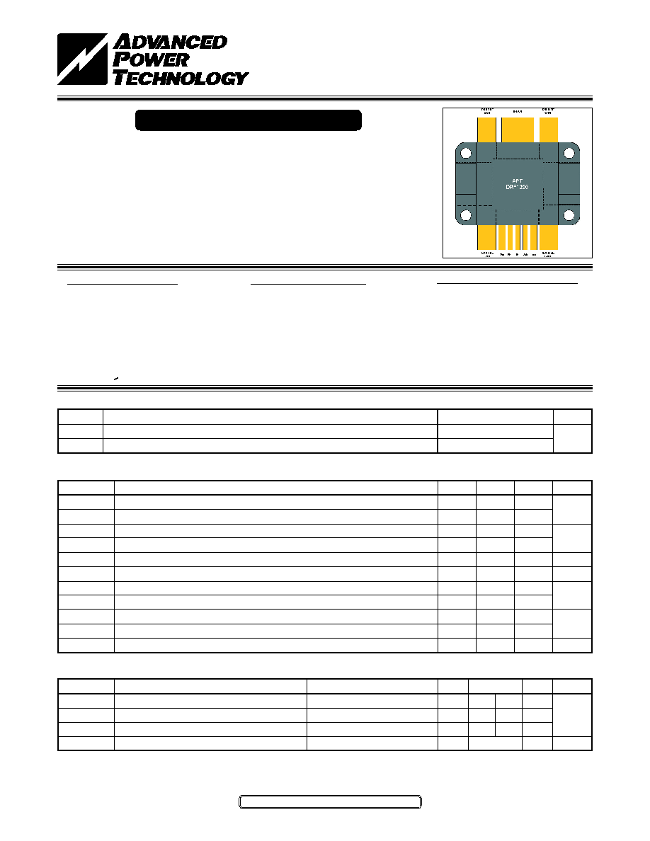
The DRF1200 MOSFET driver hybrid. This hybrid includes a high power gate driver and
the power MOSFET. It was designed to provide the system designer increased flexibility
and lowered cost over a non-integrated solution.
050-4913 Rev A 2-2006
APT Website - http://www.advancedpower.com

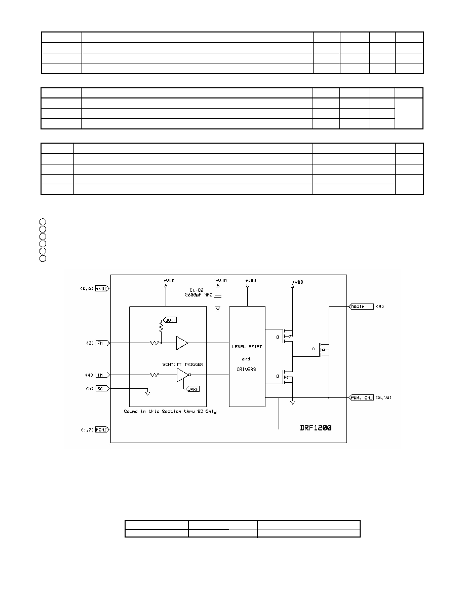
Figure 1, DRF1200 Simplified Ciruit Diagram
A Simplified DRF1200 Circuit Diagram is illustrated above. By including the driver high speed by-pass capacitors (C1-C8), their
contribution to the internal parasitic loop inductance of the driver output is greatly reduced. This, coupled with the tight geometry of the
hybrid, allows optimal the gate drive to the MOSFET. This low parasitic approach, coupled with the Schmitt trigger input, Kelvin signal
ground and the Anti-Ring Function, Provide improved stability and control in Kilowatt to Multi-Kilowatt, High Frequency applications.
The IN pin is the input for the control signal and is applied to a Schmitt Trigger. The signal is then applied to the intermediate drivers
and level shifters; this section contains proprietary circuitry designed specifically for ring abatement. The P channel and N channel
power drivers provide the high current to the gate of the MOSFET and the MOSFET drain is attached to the OUT pin (9).
Driver Control Logic
In (4) HIGH Driver
Driver Output LOW
MOSFET OFF Drain (9) HIGH
In (4) LOW Driver
Driver Output HIGH
MOSFET ON Drain (9) LOW
The FUNCTION, FN, pin (3) is used to disable the Anti-Ring function. It is recommended that the device be operated with this function
enabled. Func. = Hi (+5V or Float) Anti-Ring on, Func. = Low (0V or GND.) Anti-ring off.
On the Output side are the POWER GROUND connections pin 8 and pin 10. The DRAIN connection is pin 9. It is suggested that
output currents be restricted to these pins by design.
MOSFET Absolute Maxumum Ratings
Thermal Characteristics
Dynamic Characteristics
Test curcuit show on page 3.
All measurements were made with the Anti-Ring circuit activated unless noted.
1. Symmetry is the percent difference in high and low FWHM times with a 50% duty cycle square wave input.
2 R
L
= 50, C
L
= 3000pF
3 10% - 90% See Test Circuit
4 50% - 50%, see Test Circuit
5 V
DD
= 18V, C
L
= 3000pF, F = 10MHz
6 Performance specified with this input.
APT reserves the right to change, without notice, the specifications and information contained herein.
Unit
V
A
Unit
pF
Unit
įC/W
įC
W
Min
Typ
Max
1000
13
0.90
Ratings
0.13
175
>100
1050
Min
Typ
Max
2000
165
75
Parameter
Drain-Source Voltage
Continuos Drain Current T
HS
= 25įC
Drain-Source On State Resistance
Characteristic
Junction to Case Thermal Resistance
Operating and Storage Junction Temperature
Maximum Power Dissipation
Total Power Dissipation @ T
C
= 25įC
Parameter
Input Capacitance
Output Resistance
Reverse Transfer Capacitance
Symbol
V
DSS
I
D
R
DS(on)
Symbol
R
JC
T
J
P
D
P
DC
Symbol
C
iss
C
oss
C
rss
050-4913 Rev A 2-2006
DRF1200

The Test Circuit illustrated above was used to evaluate the DRF1200 (available as an evaluation Board DRF1200
EVAL). The input control signal is applied to the DRF1200 via IN(4) and SG(5) pins using RG188. This provides excel-
lent noise immunity and control of the signal ground currents.
The FN pin is very sensitive and unwanted signals can cause erratic behavior, Therefore FN pin is heavily by-passed
on the Evaluation board, see FN (3) above.
The +VDD inputs (2,6) are By-Passed (C1-C3, C5-C7), this is in addition to the internal bypassing mentioned previ-
ously. The capacitors used for this function must be capable of supporting the RMS currents and frequency of the gate
load.
A 50 (R4) load is used evaluate the output performance of the DRF1200.
Figure 2, Test Circuit
050-4913 Rev A 2-2006
DRF1200

Figure 3, Drain & Current Waveforms
Figure 4, Drain Fall Time
In Figure 3 we see a drain voltage fall of 800V and the current rise of 13.6A in a 50 Load. The drain voltage fall time is 3.4ns 10%
to 90% as shown in Figure 4.
Figure 5, Typical Capacitance vs. Drain-to-Source Voltage
Figure 6, Typical Maximum Safe Operating Area
Figure 7, Maximum Effective Transient Thermal Impedance, Junction-to -Case vs. Pulse Duration
050-4913 Rev A 2-2006
DRF1200

0.100
0.040
0.300
.005in. Typ. Half Hard
Copper Gold Plated
1.500
1.00
0.06
0.04
1.25
0.750
0.300
0.300
0.275
0.200
0.369
0.200
0.275
5600
5600
5600
5600
5600
5600
5600
5600
APT
DRF1200
.115 in. Clear 4 Places
.090 Gap
Typ.
.050 Gap Typ.
GND
+V
DD
FN IN SG +V
DD
+V
DD
1
2
3
4
5
6
7
DRAIN
SOURCE
GND
SOURCE
GND
10
9
8
GND
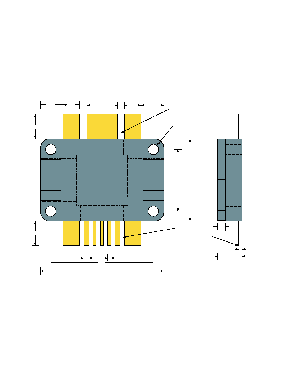
Figure 8, DRF1200 Mechanical Outline
050-4913 Rev A 2-2006
DRF1200

HV By-Pass Capacitors
Load Resistors
+Vdd By-Pass Capacitors
+Vdd By-Pass Capacitors
Vds Monitor
Control In
FN By-Pass
Decoupling Resistors
Control In 50
Terminator
This Section Configured by User
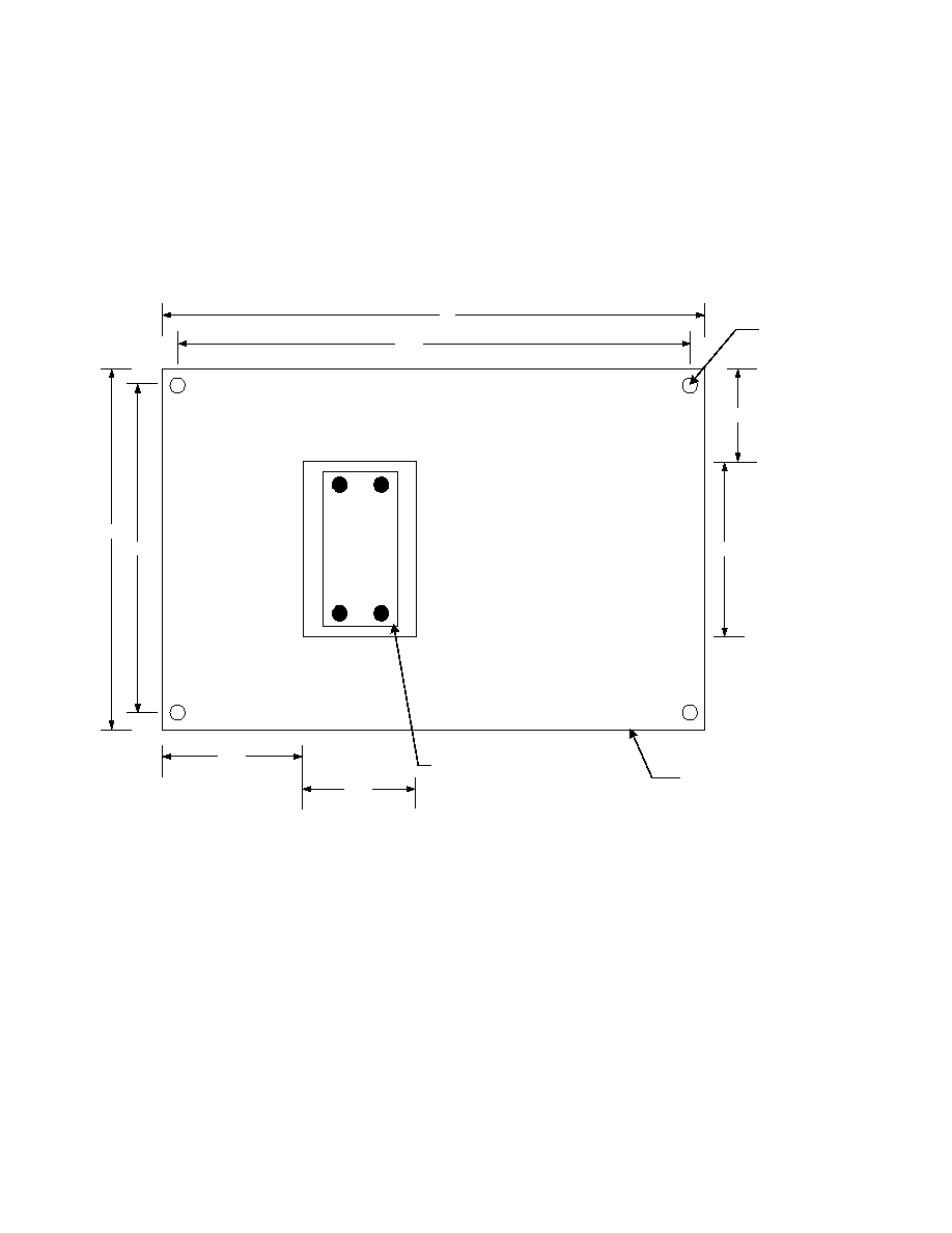
Figure 9, DRF1200 Eval Board
The DFR1200 is a high power device and must have adequate cooling for full power operation
Evaluation Boards are provided to facilitate the circuit design process by allowing the end user to quickly
evaluate the performance of our components under a specific and single set of conditions. They are not
intended to be used as a sub assembly in any final product(s). Care has been taken to insure that the
Evaluation Boards are assembled to correctly represent the test circuit included in the component data
sheet. There is no warranty of these Evaluation Boards beyond workmanship and materials.
050-4913 Rev A 2-2006
DRF1200

5.196
5.5
3.196
1.425
1.145
1.7
0.900
Advanced Power Technology DRF1200
RE 12/06/05 revD
3.50
See DRF1200 mechanical drawing
for physical dimension details
PCB material - .062 FR4
4 holes .150 dia.
Figure 10, DRF1200 Eval Board Mechanical
050-4913 Rev A 2-2006
DRF1200

Mounting instructions for Flangeless Packages
Heat sink mounting of any device in the Flangeless Package family follows the same
process details outlined in this document.
Heat Sink Surface:
1. The heat sink surface should be smooth, free
of nicks and burs; in addition it should be flat to
.001in./in TIR, (Total Indicator Run out) and be
finished to ~ 68Ķ CLA, (Center Line Average).
2. Must be free of solder balls, metal shavings and
any foreign objects or material.
Device Preparation:
1. The leads should be prepared with an "s" bend, as
shown in Figure 10 prior to mounting on the heat sink
2. The BeO surface of the device must be
free of any foreign objects or material.
3. The BeO surface must be coated with a
thin and uniform film of thermal compound.
4. For commercial manufacturing the
suggested method for thermal compound
application is to apply the compound using
a screen printer. This process insures con-
sistent and repeatable performance with
minimum effort.
Mechanical Attachment:
1. The four screws (1-2-3-4), as shown in
Figure 11, should be installed and seated,
then torqued to one-half the specification,
in the sequence shown. First screw 1 then
screw 2, 3 and 4.
2. Then complete the process by tighten-
ing to the full specification in the same
manner.
3. The torque spec is 8in.lb. Ī1lb. (0.9Nm)
Lead Attachment:
1. The leads may now be soldered to the
PCB
2. Maximum lead temperature must not
exceed 300įC for 10s.
3. For lead free use 96.5 % tin, 3% silver,
and 0.5% copper.
4. Non-lead Free use 2% Silver, 62% Tin,
36% lead (sn62).
Figure 11, Top and Side View of a T3 device
Figure 12, Stress Relief bend
Thermal Compound
#4 Flat Washer
4-40 Socket head SS Screws .
Torque to 8in.lb.
PCB
T3 Package
1
2
3
4
Torque screws in 1 -2-3-4 Sequence
PCB
Stress Relief
"S" Bend
On all leads
PCB
Stress Relief
"S" Bend
On all leads
050-4913 Rev A 2-2006
DRF1200
