
MSC1075MP
Advanced Power Technology reserves the right to change, without notice, the specifications and information contained herein
Visit our website at WWW.ADVANCEDPOWER.COM or contact our factory direct.
DESCRIPTION:
The MSC1075MP is a gold-metallized silicon, NPN power transistor
designed for applications requiring high peak power and low duty
cycles, such as IFF, DME, and TACAN. It is packaged in the .280"
input-matched stripline flange package, resulting in improved
broadband performance and low thermal resistance.
ABSOLUTE MAXIMUM RATINGS (Tcase = 25
∞
C)
Symbol
Parameter
Value
Unit
V
CBO
Collector-Base Voltage
65
V
V
CES
Collector-Emitter Voltage
65
V
V
EBO
Emitter-Base Voltage
3.5
V
I
C
Device Current
5.5
A
P
DISS
Power Dissipation
218.7
W
T
J
Junction Temperature
+ 200
∞
∞
C
T
STG
Storage Temperature
≠65 to +150
∞
∞
C
THERMAL DATA
R
TH(j-c)
Junction-Case Thermal Resistance
0.8
∞
∞
C/W
Features
Features
∑
DESIGNED FOR HIGH POWER PULSED IFF, DME,
TACAN APPLICATIONS
∑
80 W (typ.) IFF 1030 ≠ 1090 MHz
∑
75 W (min.) DME 1025 ≠ 1150 MHz
∑
50 W (typ.) TACAN 960 ≠1215 MHz
∑
8.0 dB MIN. GAIN
∑
REFRACTORY GOLD METALLIZATION
∑
EMITTER BALLASTING AND LOW THERMAL
RESISTANCE FOR RELIABILITY AND RUGGEDNESS
∑
INFINITE LOAD VSWR CAPABILITY AT SPECIFIED
OPERATING CONDITIONS
∑
INPUT MATCHED COMMON BASE CONFIGURATION
RF AND MICROWAVE TRANSISTORS
HF SSB APPLICATIONS
140 COMMERCE DRIVE
MONTGOMERYVILLE, PA
18936-1013
PHONE: (215) 631-9840
FAX: (215) 631-9855
MSC1075MP
Advanced Power Technology reserves the right to change, without notice, the specifications and information contained herein
Visit our website at WWW.ADVANCEDPOWER.COM or contact our factory direct.
ELECTRICAL SPECIFICATIONS (Tcase = 25
ELECTRICAL SPECIFICATIONS (Tcase = 25
∞
∞
C)
C)
STATIC
Value
Symbol
Test Conditions
Min.
Typ.
Max.
Units
BV
CBO
I
C
= 10 mA I
E
= 0 Ma
65
V
BV
CES
I
C
= 25 mA V
BE
= 0 V
65
V
BV
EBO
I
E
= 10 mA I
C
= 0 mA
3.5
V
I
CES
V
CE
= 50 V I
E
= 0 mA
5
mA
h
FE
V
CE
= 5 V I
C
= .1 A
10
DYNAMIC
Value
Symbol
Test Conditions
Min.
Typ.
Max.
Units
P
OUT
f = 1025 ≠ 1150 MHz P
IN
= 13.0 W V
CE
= 50 V
75
W
G
P
f = 1025 ≠ 1150 MHz P
IN
= 13.0 W V
CE
= 50 V
7.5
dB
Note: Pulse width = 10µSec. Duty Cycle = 1%
This device is suitable for use under other pulse width/duty cycle conditions.
Please contact the factory for specific applications assistance.
MSC1075MP
Advanced Power Technology reserves the right to change, without notice, the specifications and information contained herein
Visit our website at WWW.ADVANCEDPOWER.COM or contact our factory direct.
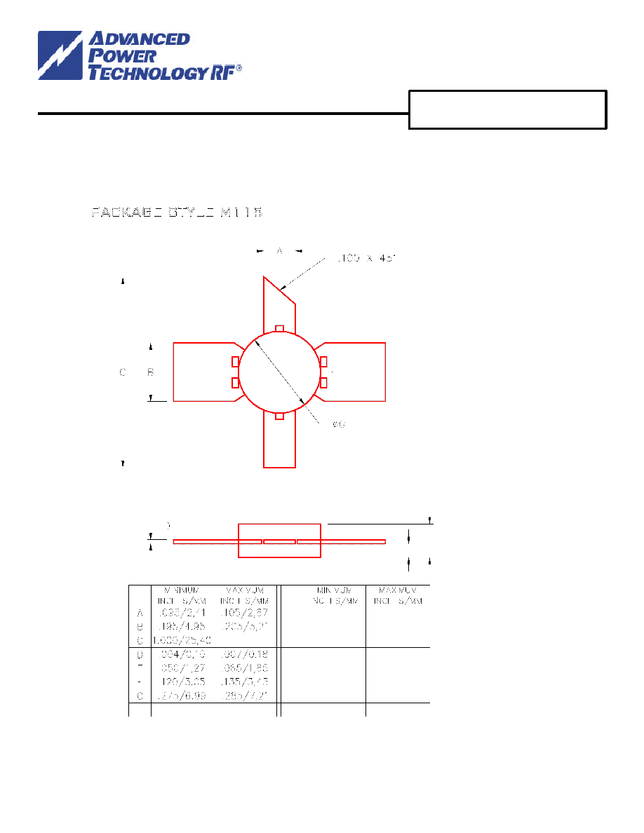
PACKAGE MECHANICAL DATA
PACKAGE MECHANICAL DATA