Preliminary Data Sheet
September 2000
LU3X34FT
Quad 3 V 10/100 Ethernet Transceiver TX/FX
Overview
The LU3X34FT is a fully integrated 4-port
10/100 Mbits/s physical layer device with transceiver.
This part was designed specifically for
10/100 Mbits/s switches. The LU3X34FT was
designed to conform fully with all pertinent specifica-
tions, from the ISO
1
/IEC
2
11801 and EIA
3
/TIA 568
cabling guidelines to ANSI
4
X3.263 TP-PMD to
IEEE
5
802.3 Ethernet specification.
Features
s
4-port, single-chip integrated physical layer and
transceivers for 10Base-T, 100Base-TX, or
100Base-FX functions
s
IEEE 802.3 compatible 10Base-T and 100Base-T
physical layer interface and ANSI X3.263 TP-PMD
compatible transceiver
s
Interface support for MII
s
Autonegotiation pin configurability on a per-port
basis
s
Combined TX, 10Base-T, FX drivers, receivers,
and signal detect circuit
s
Built-in, analog 10 Mbits/s receive filter, removing
the need for external filters
s
Built-in 10 Mbits/s transmit filter
s
10 Mbits/s PLL exceeding tolerances for both pre-
amble and data jitter
s
100 Mbits/s PLL, combined with the digital adap-
tive equalizer, robustly handles variations in rise-
fall time, excessive attenuation due to channel
loss, duty-cycle distortion, crosstalk, and baseline
wander
s
Transmit rise-fall time manipulated to provide lower
emissions, amplitude fully compatible for proper
interoperability
s
Programmable scrambler seed for better FCC
compliancy
s
IEEE 802.3u Clause 28 compliant autonegotiation
for full 10 Mbits/s and 100 Mbits/s control
s
Extended management support with interrupt
capabilities
s
PHY MIB support
s
Low-power, 480 mA max
s
Low-cost, 160 PQFP packaging
1. ISO is a registered trademark of the International Organization
for Standardization.
2. IEC is a registered trademark of The International Electrotechni-
cal Commission.
3. EIA is a registered trademark of Electronic Industries Associa-
tion.
4. ANSI is a registered trademark of American National Standards
Institute.
5. IEEE is a registered trademark of The Institute of Electrical and
Electronics Engineers, Inc.

Table of Contents
Contents
Page
LU3X34FT
Preliminary Data Sheet
Quad 3 V 10/100 Ethernet Transceiver TX/FX
September 2000
2
Lucent Technologies Inc.
Overview................................................................................................................................................................... 1
Features ................................................................................................................................................................... 1
Description................................................................................................................................................................ 4
Pin Information ......................................................................................................................................................... 5
Pin Descriptions........................................................................................................................................................ 6
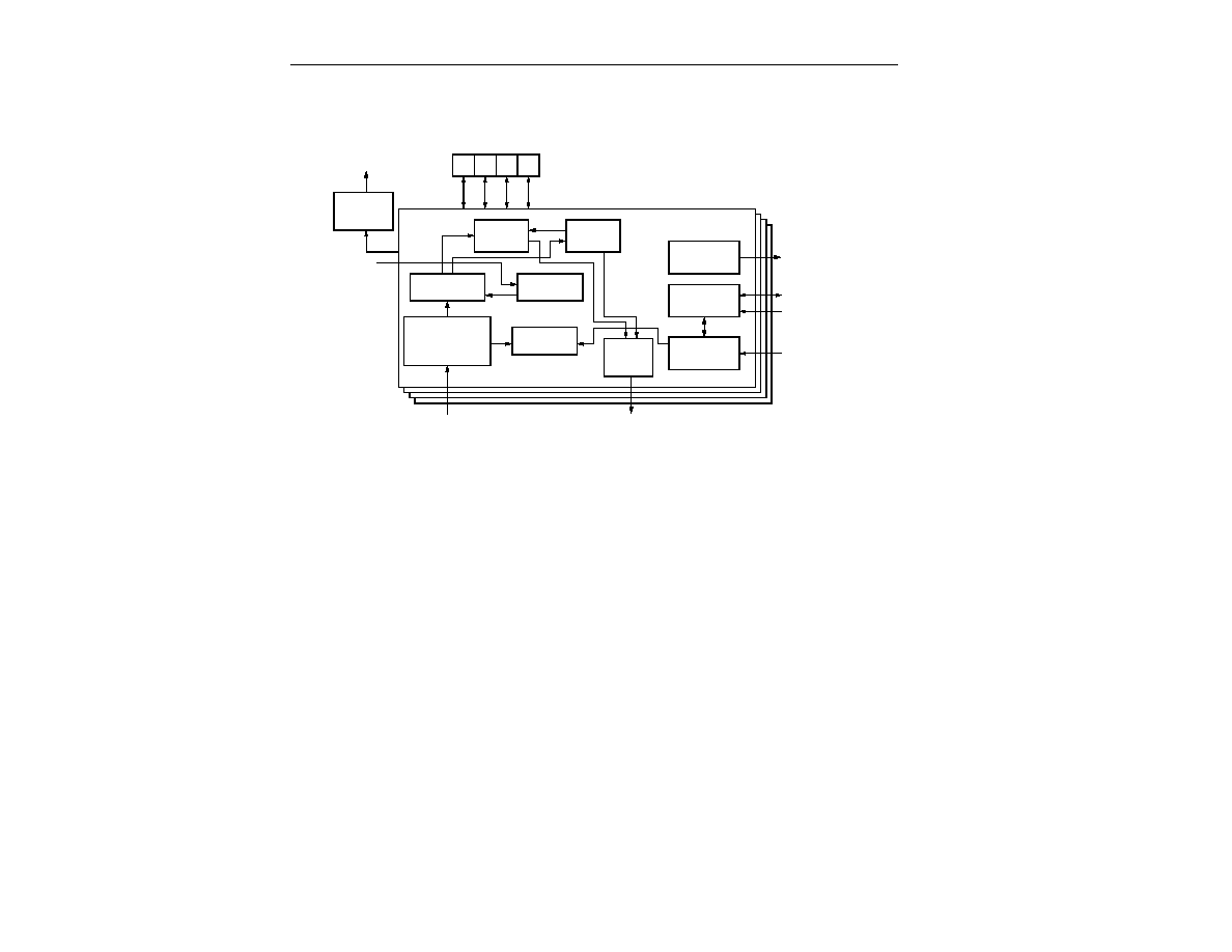
Functional Description ............................................................................................................................................ 11
Media Independent Interface (MII) ...................................................................................................................... 11
100Base-X Module.............................................................................................................................................. 12
10Base-T Module ................................................................................................................................................ 17
Clock Synthesizer................................................................................................................................................ 19
Autonegotiation ................................................................................................................................................... 19
Reset Operation .................................................................................................................................................. 20
MII Registers .......................................................................................................................................................... 23
dc and ac Specifications......................................................................................................................................... 36
Absolute Maximum Ratings................................................................................................................................. 36
Clock Timing........................................................................................................................................................... 37
Outline Diagram...................................................................................................................................................... 47
Tables
Page
Table 1. Twisted-Pair Magnetic Interface ................................................................................................................... 6
Table 2. Twisted-Pair Transceiver Control/Transmitter Control ................................................................................... 6
Table 3. MII Interface ................................................................................................................................................. 6
Table 4. Autonegotiation/LED Configuration .............................................................................................................. 8
Table 5. Special Mode Configurations ....................................................................................................................... 9
Table 6. Clock and Chip Reset .................................................................................................................................. 9
Table 7. Power and Ground .....................................................................................................................................10
Table 8. Symbol Coding Table ................................................................................................................................. 14
Table 9. Initial Values for Autonegotiation Registers ................................................................................................ 22
Table 10. MII Management Registers ...................................................................................................................... 23
Table 11. Control Register (Register 0h) ................................................................................................................. 23
Table 12. Status Register Bit Definitions (Register 1h)............................................................................................ 25
Table 13. PHY Identifier (Register 2h) ..................................................................................................................... 27
Table 14. PHY Identifier (Register 3h) ..................................................................................................................... 27
Table 15. Advertisement (Register 4h) .................................................................................................................... 27
Table 16. Autonegotiation Link Partner Ability (Register 5h) ................................................................................... 28
Table 17. Autonegotiation Expansion Register (Register 6h) ..................................................................................28
Table 18. Programmable LED (Register 11h) Only Under PHY Address for Port 2................................................. 29
Table 19. Receive Error Counter (Register 15h)......................................................................................................31
Table 20. PHY Control/Status Register (Register 17h)............................................................................................ 31
Table 21. Config 100 Register (Register 18h).......................................................................................................... 32
Table 22. PHY Address Register (Register 19h) ..................................................................................................... 33
Table 23. Config 10 Register (Register 1Ah) ........................................................................................................... 34
Table 24. Status 100 Register (Register 1Bh) ......................................................................................................... 34
Table 25. Status 10 Register (Register 1Ch) ........................................................................................................... 34
Table 26. Interrupt Mask Register (Register 1Dh) ................................................................................................... 35
Table 27. Interrupt Status Register (Register 1Eh) .................................................................................................. 35
Table 28. Absolute Maximum Ratings ..................................................................................................................... 36
Table 29. Operating Conditions ............................................................................................................................... 36
Table 30. dc Characteristics.....................................................................................................................................36

Lu
ce
nt T
e
chn
o
l
ogi
es
Inc
.
5
P
r
eli
m
inar
y
D
a
t
a
S
h
ee
t
L
U
3
X3
4FT
S
e
pt
embe
r 20
00
Q
u
ad 3
V 1
0
/1
00
Et
herne
t
T
r
a
n
sce
iv
er TX
/FX
Pin Inf
o
rm
ation
5-7
908(
F).r
4
Figur
e
2
.
P
i
n D
i
a
g
r
a
m
2
3
4
5
6
7
8
9
10
11
12
13
14
15
16
17
18
19
20
21
22
23
24
25
26
27
28
29
30
31
32
33
34
35
36
37
38
39
40
1
10F
D
_
0
RXV
DD
0
RX+_
0
R
X
≠_0
RXGND0
R
E
F
1
0
0_0
TX
+
_
0
T
X
≠_0
TXV
DD
0
TXV
DD
1
T
X
≠_1
TX
+
_
1
R
E
F
1
0
0_1
RXGND1
R
X
≠_1
RX+_
1
RXV
DD
1
REF
G
ND
CSV
DD
10
CSGND1
0
CSG
ND1
0
0
CSV
DD
100
RE
F
1
0
RXV
DD
2
RX+_
2
R
X
≠_2
RXGND2
R
E
F
1
0
0_2
TX
+
_
2
T
X
≠_2
TXV
DD
2
TXV
DD
3
T
X
≠_3
TX
+
_
3
R
E
F
1
0
0_3
RXGND3
R
X
≠_3
RX+_
3
RXV
DD
3
10F
D
_
3
120
119
118
117
116
115
114
113
112
111
110
109
108
107
106
105
104
103
102
101
100
99
98
97
96
95
94
93
92
91
90
89
88
87
86
85
84
83
82
81
TXEN_
1
TXD
_
1[
0
]
TXD
_
1[
1
]
TXD
_
1[
2
]
TXD
_
1[
3
]
IO
_
V
DD
3
I
O
_
G
ND3
TXER_
1
CR
S
_
1
/
PHY_
AD[
C
O
L_
1/10
0F
D
_
1
RXDV_
1
RXD_
1
[
0
]
DI
GV
DD
1
DI
GGND1
RXD_
1
[
1
]
RXD_
1
[
2
]
RXD_
1
[
3
]
RXER_
1
TXC
L
K_
1
RXCL
K_
1
IO
V
DD
4
I
OGND4
RXCL
K_
2
RXER_
2
RXD_
2
[
3
]
DI
GV
DD
2
DI
GGND2
RXD_
2
[
2
]
RXD_
2
[
1
]
RXD_
2
[
0
]
RXDV_
2
C
O
L_
2/10
0F
D
_
2
CR
S
_
2
/
PHY_
AD[
TXER_
2
TXD
_
2[
3
]
TXD
_
2[
2
]
TXD
_
2[
1
]
TXD
_
2[
0
]
TXEN_
2
TXC
L
K_
2
42
43
44
45
46
47
48
49
50
51
52
53
54
55
56
57
58
59
60
61
62
63
64
65
66
67
68
69
70
71
72
73
74
75
76
77
78
79
80
41
INTZ
PAUSE
TPTXTR
ISOLATE
ANEN_2/SD+_2/LED100_2
10HD_2/SD≠_2/LEDFD_2
100HD_2/LEDCOL_2
FOSEL_2/LEDLNK_2
LEDGND2
LEDV
DD
2
ANEN_3/SD+_3/LED100_3
10HD_3/SD≠_3LEDFD_3
100HD_3/LEDCOL_3
FOSEL_3/LEDLNK_3
TXEN_3
TXD_3[0]
TXD_3[1]
TXD_3[2]
TXD_3[3]
TXER_3
COL_3/100FD_3
CRS_3/PHY_AD[4]
MDC
MDIO
SUBGND2
HSV
DD
2
HSGND2
TMGND1
IOGND6
TXCLK_3
IOV
DD
6
RXDV_3
RXD_3[0]
RXD_3[1]
RXD_3[2]
RXD_3[3]
RXER_3
RXCLK_3
IOGND5
IOV
DD
5
LU
3X
3
4
F
T
16
0 P
Q
F
P
160
159
158
157
156
155
154
153
152
151
150
149
148
147
146
145
144
143
142
141
140
139
138
137
136
135
134
133
132
131
130
129
128
127
126
125
124
123
122
121
RSTZ
TESTMSEL
FOSEL_1/LEDLNK_1
100HD_1/LEDCOL_1
10HD_1/SD≠_1/LEDFD_1
ANEN_1/SD+_1/LED100_1
LEDV
DD
1
LEDGND1
FOSEL_0/LEDLNK_0
100HD_0/LEDCOL_0
10HD_0/SD≠_0/LEDFD_0
ANEN_0/SD+_0/LED100_0
CLK_25
TXEN_0
TXD_0[0]
TXD_0[1]
TXD_0[2]
TXD_0[3]
ER
TXER_0
IOV
DD
1
IOGND1
TXCLK_0
SUBGND1
CRS_0
COL_0/100FD_0
RXDV_0
RXD_0[0]
HSV
DD
1
HSGND1
TMV
DD
1
RXD_0[1]
RXD_0[2]
RXD_0[3]
RXER_0
RXCLK_0
IOV
DD
2
IOGND2
10FD_1
10FD_2