 | –≠–Ľ–Ķ–ļ—ā—Ä–ĺ–Ĺ–Ĺ—č–Ļ –ļ–ĺ–ľ–Ņ–ĺ–Ĺ–Ķ–Ĺ—ā: LU3X51FT | –°–ļ–į—á–į—ā—Ć:  PDF PDF  ZIP ZIP |
Document Outline
- Features
- Description
- Pin Information
- MII Station Management
- Absolute Maximum Ratings (TA = 25 įC)
- Electrical Characteristics
- Timing Characteristics (Preliminary)
- Outline Diagram
- Ordering Information
- List of Figures
- Figure 1 . Functional Block Diagram
- Figure 2 . Typical Twisted-Pair (TP) Interface
- Figure 3 . Fiber-Optic Interface
- Figure 4 . 100-Pin Preliminary Pinout
- Figure 5 . MDIO Input Timing
- Figure 6 . MDIO Output Timing
- Figure 7 . MDIO During TA (Turnaround) of a Read Transaction
- Figure 8 . MII Timing Requirements for LU3X51FT
- Figure 9 . Serial 10 Mbits/s Timing for TPINĪ, CRS, and RX_CLK
- Figure 10 . Serial 10 Mbits/s Timing for TX_EN, TPOUTĪ, CRS, and RX_CLK
- Figure 11 . Serial 10 Mbits/s Timing for TX_EN, TPINĪ, and COL
- Figure 12 . Serial 10 Mbits/s Timing for RX_CLK, CRS, RXD, TX_CLK, TX_EN, and TXD
- Figure 13 . Serial 10 Mbits/s Timing Diagram for RX_CLK and TX_CLK
- Figure 14 . 100 Mbits/s MII Transmit Timing
- Figure 15 . 100 Mbits/s MII Receive Timing
- List of Tables
- Table 1. LU3X51FT Crystal Specifications
- Table 2. MII/5-Bit Serial Interface Pins (19)
- Table 3. MII Management Pins (3)
- Table 4. 10/100 Mbits/s Twisted-Pair (TP) Interface Pins (7)
- Table 5. Clock Pins (6)
- Table 6. Control/Status Pins (18)
- Table 7. Power and Ground Pins (47)
- Table 8. MII Management Frame Format
- Table 9. MII Management FramesĄField Descriptions
- Table 10. MII Management Registers (MR)
- Table 11. MR0ĄControl Register Bit Descriptions
- Table 12. MR1ĄStatus Register Bit Descriptions
- Table 13. MR2, 3ĄPHY Identifier Registers (1 and 2) Bit Descriptions
- Table 14. MR4ĄAutonegotiation Advertisement Register Bit Descriptions
- Table 15. MR5ĄAutonegotiation Link Partner Ability Register Bit Descriptions
- Table 16. MR5ĄAutonegotiation Link Partner Ability Register (Next Page) Bit Descriptions
- Table 17. MR6ĄAutonegotiation Expansion Register Bit Descriptions
- Table 18. MR7ĄNext Page Transmit Register Bit Descriptions
- Table 19. MR28ĄDevice Specific Register 1 (Status Register) Bit Descriptions
- Table 20. MR29ĄDevice Specific Register 2 (100 Mbits/s Control) Bit Descriptions
- Table 21. MR30ĄDevice Specific Register 3 (10 Mbits/s Control) Bit Descriptions
- Table 22. MR31ĄQuick Status Register Bit Descriptions
- Table 23 . Absolute Maximum Ratings
- Table 24 . Operating Conditions
- Table 25. dc Characteristics
- Table 26. MII Management Interface Timing (25 pF Load)
- Table 27. MII Data Timing (25 pF Load)
- Table 28. Serial 10 Mbits/s Timing for TPINĪ, CRS, and RX_CLK
- Table 29. Serial 10 Mbits/s Timing for TX_EN, TPOUTĪ, CRS, and RX_CLK
- Table 30. Serial 10 Mbits/s Timing for TX_EN, TPINĪ, and COL
- Table 31. Serial 10 Mbits/s Timing for RX_CLK, CRS, RXD, TX_CLK, TX_EN, and TXD (25 pF Load)
- Table 32. Serial 10 Mbits/s Timing for RX_CLK and TX_CLK (25 pF Load)
- Table 33. 100 Mbits/s MII Transmit Timing
- Table 34. 100 Mbits/s MII Receive Timing
- Contact Us

Data Sheet
July 2000
LU3X51FT
FASTCAT
TM
Ethernet Transceiver 10/100Base-TX/FX
Features
10 Mbits/s Transceiver
s
Compatible with
IEEE
* 802.3 10Base-T standard
for twisted-pair cable
s
Autopolarity detection and correction
s
Adjustable squelch level for extended wire-length
capability (two levels)
s
Interfaces with
IEEE
802.3u media independent
interface (MII) or a serial 10 Mbits/s 7-pin interface
s
On-chip filtering, eliminating the need for external
filters
s
Half- and full-duplex operations
100 Mbits/s TX Transceiver
s
Compatible with
IEEE
802.3u MII (clause 22), PCS
(clause 23), PMA (clause 24), autonegotiation
(clause 28), and PMD (clause 25) specifications
s
Scrambler/descrambler bypass
s
Encoder/decoder bypass
s
3-statable MII in 100 Mbits/s mode
s
Selectable carrier sense signal generation (CRS)
asserted during either transmission or reception in
half duplex (CRS asserted during reception only in
full duplex)
s
Selectable MII or 5-bit code group interface
s
Full- or half-duplex operations
s
Optional carrier integrity monitor (CIM)
s
On-chip filtering and adaptive equalization, elimi-
nating the need for external filters
*
IEEE
is a registered trademark of The Institute of Electrical and
Electronics Engineers, Inc.
100 Mbits/s FX Transceiver
s
Compatible with
IEEE
802.3u 100Base-FX stan-
dard
s
Reuses existing twisted-pair I/O pins for compati-
ble fiber-optic transceiver pseudo-ECL (PECL)
data with no additional data pins required
s
Fiber mode automatically configures port:
-- Disables autonegotiation
-- Disables 10Base-T
-- Enables 100Base-FX remote fault signaling
-- Disables MLT-3 encoder/decoder
-- Disables scrambler/descrambler
s
FX mode enable is pin- or register-selectable
General
s
10 Mbits/s and 100 Mbits/s outputs multiplexed to a
single 1:1 transformer, eliminating the need for
external relays or switches
s
Independent powerdown for 10 Mbits/s and
100 Mbits/s
s
Single 25 MHz crystal input, or 25 MHz clock input,
optional 20 MHz clock input
s
Autonegotiation (
IEEE
802.3u, clause 28):
-- Fast link pulse (FLP) burst generator
-- Parallel detection for 10 Mbits/s and 100 Mbits/s
-- Arbitration function
s
Supports the MII station management protocol and
frame format (clause 22):
-- Basic and extended registers
-- Supports next page function
-- Accepts preamble suppression
-- Two modes of operation: asynchronous from
0 MHz to 6.5 MHz and synchronous from
6.5 MHz to 12.5 MHz
-- Provides maskable status interrupt signals
Note: Advisories are issued as needed to update product information. When using this data sheet for design purposes, please contact
your Lucent Technologies Microelectronics Group Account Manager to obtain the latest advisory on this product.

Table of Contents
Contents
Page
LU3X51FT
Data Sheet
FASTCAT Ethernet Transceiver 10/100Base-TX/FX
July 2000
2
Lucent Technologies Inc.
Features ................................................................................................................................................................... 1
10 Mbits/s Transceiver ............................................................................................................................................ 1
100 Mbits/s TX Transceiver ..................................................................................................................................... 1
100 Mbits/s FX Transceiver ..................................................................................................................................... 1
General ................................................................................................................................................................... 1
Description ............................................................................................................................................................... 4
Clocking .................................................................................................................................................................. 4
FX Mode ................................................................................................................................................................. 5
Twisted-Pair (TP) Interface Application Diagram..................................................................................................... 6
Fiber-Optic Interface Application Diagram .............................................................................................................. 7
Pin Information ......................................................................................................................................................... 8
Preliminary Pin Diagram ......................................................................................................................................... 8
Pin Descriptions ...................................................................................................................................................... 9
MII Station Management ........................................................................................................................................ 17
Basic Operations................................................................................................................................................... 17
MII Management Frames ...................................................................................................................................... 17
Management Registers (MR) ................................................................................................................................ 18
Absolute Maximum Ratings (TA = 25
į
C) ............................................................................................................... 29
Electrical Characteristics ........................................................................................................................................ 29
Timing Characteristics (Preliminary) ...................................................................................................................... 30
Outline Diagram ...................................................................................................................................................... 39
100-Pin TQFP ....................................................................................................................................................... 39
Ordering Information ............................................................................................................................................... 40
Table 1. LU3X51FT Crystal Specifications .............................................................................................................. 4
Table 2. MII/5-Bit Serial Interface Pins (19) ............................................................................................................. 9
Table 2. MII/5-Bit Serial Interface Pins (19) (continued) ........................................................................................ 10
Table 3. MII Management Pins (3)......................................................................................................................... 11
Table 4. 10/100 Mbits/s Twisted-Pair (TP) Interface Pins (7) ................................................................................. 12
Table 5. Clock Pins (6) ........................................................................................................................................... 13
Table 6. Control/Status Pins (18) ........................................................................................................................... 14
Table 6. Control/Status Pins (18) ........................................................................................................................... 15
Table 7. Power and Ground Pins (47) .................................................................................................................... 16
Table 6. Control/Status Pins (18) ........................................................................................................................... 16
Table 8. MII Management Frame Format............................................................................................................... 17
Table 9. MII Management Frames--Field Descriptions ......................................................................................... 17
Table 10. MII Management Registers (MR) ........................................................................................................... 18
Table 11. MR0--Control Register Bit Descriptions ................................................................................................ 19
Table 12. MR1--Status Register Bit Descriptions ................................................................................................. 20
Table 13. MR2, 3--PHY Identifier Registers (1 and 2) Bit Descriptions ................................................................ 21
Table 14. MR4--Autonegotiation Advertisement Register Bit Descriptions........................................................... 21
Table 15. MR5--Autonegotiation Link Partner Ability Register Bit Descriptions.................................................... 22
Table 16. MR5--Autonegotiation Link Partner Ability Register (Next Page) Bit Descriptions................................ 22
Table 17. MR6--Autonegotiation Expansion Register Bit Descriptions ................................................................. 23
Table 18. MR7--Next Page Transmit Register Bit Descriptions............................................................................. 24
Table 19. MR28--Device Specific Register 1 (Status Register) Bit Descriptions .................................................. 25
Table 20. MR29--Device Specific Register 2 (100 Mbits/s Control) Bit Descriptions............................................ 26
Table 21. MR30--Device Specific Register 3 (10 Mbits/s Control) Bit Descriptions.............................................. 27
Table 22. MR31--Quick Status Register Bit Descriptions ..................................................................................... 28
Table 23 . Absolute Maximum Ratings .................................................................................................................. 29
Table 24 . Operating Conditions ............................................................................................................................ 29
Table 25. dc Characteristics................................................................................................................................... 29
Table 26. MII Management Interface Timing (25 pF Load) .................................................................................... 30

Lucent Technologies Inc.
3
Data Sheet
LU3X51FT
July 2000
FASTCAT Ethernet Transceiver 10/100Base-TX/FX
Table of Contents
Tables
Page
Table 27. MII Data Timing (25 pF Load) .................................................................................................................31
Table 28. Serial 10 Mbits/s Timing for TPINĪ, CRS, and RX_CLK.........................................................................33
Table 29. Serial 10 Mbits/s Timing for TX_EN, TPOUTĪ, CRS, and RX_CLK .......................................................33
Table 30. Serial 10 Mbits/s Timing for TX_EN, TPINĪ, and COL ...........................................................................34
Table 31. Serial 10 Mbits/s Timing for RX_CLK, CRS, RXD, TX_CLK, TX_EN, and TXD (25 pF Load)................35
Table 32. Serial 10 Mbits/s Timing for RX_CLK and TX_CLK (25 pF Load) ..........................................................36
Table 33. 100 Mbits/s MII Transmit Timing .............................................................................................................37
Table 34. 100 Mbits/s MII Receive Timing..............................................................................................................38
Figures
Page
Figure 1. Functional Block Diagram ......................................................................................................................... 5
Figure 2. Typical Twisted-Pair (TP) Interface ............................................................................................................ 6
Figure 3. Fiber-Optic Interface ................................................................................................................................. 7
Figure 4. 100-Pin Preliminary Pinout ....................................................................................................................... 8
Figure 5. MDIO Input Timing ..................................................................................................................................30
Figure 6. MDIO Output Timing ...............................................................................................................................30
Figure 7. MDIO During TA (Turnaround) of a Read Transaction ............................................................................30
Figure 8. MII Timing Requirements for LU3X51FT ................................................................................................32
Figure 9. Serial 10 Mbits/s Timing for TPINĪ, CRS, and RX_CLK.........................................................................33
Figure 10. Serial 10 Mbits/s Timing for TX_EN, TPOUTĪ, CRS, and RX_CLK .....................................................33
Figure 11. Serial 10 Mbits/s Timing for TX_EN, TPINĪ, and COL .........................................................................34
Figure 12. Serial 10 Mbits/s Timing for RX_CLK, CRS, RXD, TX_CLK, TX_EN, and TXD ...................................35
Figure 13. Serial 10 Mbits/s Timing Diagram for RX_CLK and TX_CLK ...............................................................36
Figure 14. 100 Mbits/s MII Transmit Timing ...........................................................................................................37
Figure 15. 100 Mbits/s MII Receive Timing ............................................................................................................38

LU3X51FT
Data Sheet
FASTCAT Ethernet Transceiver 10/100Base-TX/FX
July 2000
4
Lucent Technologies Inc.
Features
(continued)
s
Provides the following management functions via
pins if MII station management is unavailable:
-- Speed select
-- Carrier integrity enable
-- Encoder/decoder bypass
-- Scrambler/descrambler bypass
-- Full-duplex operation
-- No link pulse mode
-- Carrier sense select
-- Autonegotiation enable
-- 10 Mbits/s repeater reference clock select
-- External 20 MHz clock select
-- FX mode select
s
Provides six status signals: receive activity, transmit
activity, full duplex, collision/jabber, link integrity, and
speed indication
s
Optional LED pulse stretching
s
Powerdown mode for 10 Mbits/s and 100 Mbits/s
operation
s
PHY isolate allows single-transceiver testing when
multiple transceivers are bused together.
s
Loopback testing for 10 Mbits/s and 100 Mbits/s
operation
s
0.35
Ķ
m
low-power CMOS technology
s
Single 5 V power supply
s
100-pin TQFP
Description
The LU3X51FT is a 10/100 Mbits/s transceiver device
that supports transmission and reception over:
s
Category 3 unshielded twisted-pair (UTP) cable,
according to
IEEE
802.3 10Base-T specifications.
s
Category 5 UTP cable, according to
IEEE
802.3u
100Base-TX specifications.
s
Fiber-optic cable according to
IEEE
802.3u
100Base-FX specifications.
This transceiver interfaces to the twisted-pair media via
simple a 1:1 isolation transformer and requires no
external filter.
It also supports autonegotiation according to
IEEE
802.3u, clause 38, and the MII management interface
according to
IEEE
802.3u, clause 22.
The LU3X51FT has been designed specifically for
applications that support 10Base-T, 100Base-TX, and
100Base-FX such as network interface cards (NICs)
switches (such as Lucent Technologies Microelectron-
ics Group's LU3M38), and repeaters.
This device operates from a 5 V supply.
Figure 1 shows a functional block diagram of the
LU3X51FT device.
Clocking
The LU3X51FT requires an internal 25 MHz clock and
a 20 MHz clock to run the 100Base-TX transceiver and
10Base-T transceiver.
These clocks can be supplied as follows:
s
As separate clock inputs: 25 MHz and 20 MHz.
s
The 20 MHz clock can be internally synthesized from
the 25 MHz clock.
s
The 25 MHz clock can also be internally generated
by an on-chip oscillator if an external crystal is sup-
plied.
The LU3X51FT will automatically detect if a 25 MHz
clock is supplied, or if a crystal is being used to gener-
ate the 25 MHz clock.
Either the on-chip 20 MHz clock synthesizer (default
clock) can be used, or CLK20_SEL (pin 77) can be
pulled high (sensed on powerup and reset) to select
the external 20 MHz clock input.
The crystal specifications for the device are listed in
Table 1, and the crystal circuit is shown in Figure 2 and
Figure 3.
Table 1. LU3X51FT Crystal Specifications
Parameter
Requirement
Type
Quartz Fundamental Mode
Frequency
25 MHz
Stability
Ī25 ppm, 0--70 įC
Shunt Capacitor
7 pF
Load Capacitor
20 pF
Series Resistance
<30 ĺ

Lucent Technologies Inc.
5
Data Sheet
LU3X51FT
July 2000
FASTCAT Ethernet Transceiver 10/100Base-TX/FX
Description
(continued)
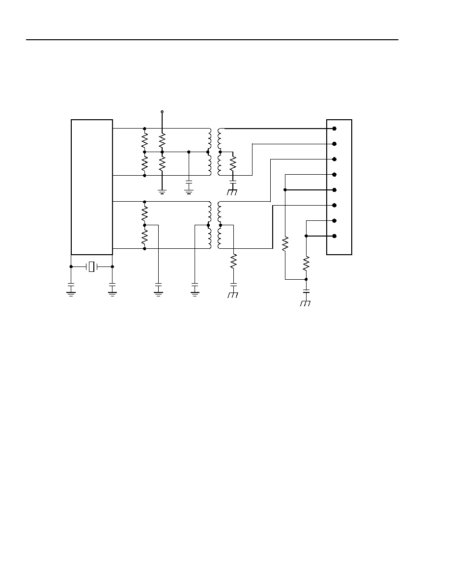
FX Mode
The LU3X51FT can operate in 100Base-FX mode by
selecting it through FX_MODE_EN, or through the reg-
ister bit (register 29, bit 0).
When operating in FX mode, the twisted-pair I/O pins
are reused as the fiber-optic transceiver I/O data pins,
and the fiber-optic signal detect (FOSD) input is
enabled.
The block diagram illustrated in Figure 1 shows a typi-
cal FX port interface. Note that no additional external
components, excluding those needed by the fiber
transceiver, are required. FX mode can operate in full
or half duplex.
When a port is placed in FX mode, it will automatically
configure the port for 100Base-FX operation (and the
register bit control will be ignored) such that:
s
The far-end fault signaling option will be enabled.
s
The MLT-3 encoding/decoding will be disabled.
s
Scrambler/descrambler will be disabled.
s
Autonegotiation will be disabled.
s
The signal detect inputs will be activated.
s
10Base-T will be disabled.
5-5136(F).ir1
Figure 1. Functional Block Diagram
AUTONEGOTIATION
AND LINK MONITOR
100 OFF
TXD[3:0]
4B/5B
ENCODER
FAR-END
FAULT GEN
SCRAMBLER
PDT
DCRU
SD
PDR
DESCRAMBLER
ALIGNER
5B/4B
DECODER
FAR-END
FAULT DETECT
10 Mbits/s TRANSCEIVER
RX_CLK
RXD[0]
TX_CLK
TX_EN
TXD[0]
CLK20
MDC
MDIO
MII
TPIN
Ī
TX STATE
MACHINE
SD
COLLISION
DETECT
SD
RX STATE
MACHINE
MII
TX_ER/TXD[4]
TX_EN
TXD[3:0]
TX_CLK
RX_CLK
RX_ER/RXD[4]
RX_DV
RXD[3:0]
COL
CRS
REF10
MANAGEMENT
25 MHz
125 MHz
LSCLK
PMD
TX/
PMD
RX/
SD
TPOUT
Ī
100 Mbits/s TRANSCEIVER
LC10 LS10
LC100
LS100
CARRIER
CIM
DETECT
RXERR_ST
CAR_STAT
MI
I
INTE
RFA
C
E
SE
RIA
L
INTE
RFA
C
E
DPLL
25 MH
Z
MA
NAG
E
ME
NT
IN
T
E
R
F
A
C
E
20 MHz
25 MHz
CRYSTAL
FIBER PORT
FX_MODE_EN
FX_MODE_EN
FIBER
PORT
FOSD
LU3X51FT
Data Sheet
FASTCAT Ethernet Transceiver 10/100Base-TX/FX
July 2000
6
Lucent Technologies Inc.
Description
(continued)
Twisted-Pair (TP) Interface Application Diagram
5-5433(F).g
Figure 2. Typical Twisted-Pair (TP) Interface
LU3X51FT
RJ-45
1
2
3
4
5
6
7
8
75
75
0.01
Ķ
F
1:1
1:1
0.01
Ķ
F
0.01
Ķ
F
0.01
Ķ
F
220
TPIN+
TPIN≠
TPOUT+
TPOUT≠
220
50
50
V
DDO
75
0.01
Ķ
F
75
XT
ALO
U
T
XT
ALI
N
38
39
33 pF
33 pF
25 MHz
50
50
0.01
Ķ
F

Lucent Technologies Inc.
7
Data Sheet
LU3X51FT
July 2000
FASTCAT Ethernet Transceiver 10/100Base-TX/FX
Description
(continued)
Fiber-Optic Interface Application Diagram
5-5433(F).h
Figure 3. Fiber-Optic Interface
LU3X51FT
TD
TDN
SD
RD
RDN
0.01
Ķ
F
220
TPIN+
TPIN≠
TPOUT+
TPOUT≠
220
50
50
V
DDO
82
0.01
Ķ
F
130
XT
ALO
U
T
XT
ALI
N
38
39
33 pF
33 pF
25 MHz
FOSD
50
50
82
130
82
130
V
DDA
0.01
Ķ
F

LU3X51FT
Data Sheet
FASTCAT Ethernet Transceiver 10/100Base-TX/FX
July 2000
8
Lucent Technologies Inc.
Pin Information
Preliminary Pin Diagram
5-6493(F).r3
Figure 4. 100-Pin Preliminary Pinout
V
SS
V
SS
V
SS
MA
SK_
ST
A
T
_INT/
P
HY
ADD[2]
PHY
A
DD[
1]
V
DD
A
V
SS
IS
OL
A
T
E
_
MO
D
E
MO
DE
_SELE
C
T
[
0]
MO
DE
_SELE
C
T
[
1]
V
SS
MO
DE
_SELE
C
T
[
2]
V
SS
FO
S
D
V
DDA
BGREF_100
V
SS
TPIN≠/FOIN≠
TPIN+/FOIN+
V
DDA
BGREF_10
V
DDA
V
SS
V
DDA
V
SS
V
DDD
V
SS
V
DDO
TPOUT≠/FOOUT≠
TPOUT+/FOOUT+
V
SS
V
DDA
ISET_100
ISET_10
V
SS
V
SS
V
DDA
V
SS
V
SS
V
DD
A
NO
_
L
P
V
DD
A
FX
_MODE
_
EN
V
SS
SE
RI
A
L_SE
L
CA
RI
N_E
N
AU
T
O
_
E
N
CRS
_SE
L
V
DDD
CK
REF
X
T
LOUT
X
T
LI
N/LSCLK
V
SS
V
SS
CLK
20
V
SS
REF10
V
DDD
V
SS
MD
I
O
V
DDD
MDC
V
SS
RXD[3]
RXD[2]
V
DDD
RXD[1]
V
SS
RXD[0]
RX_CLK
RX_ER/RXD[4]
V
DDD
RX_DV
COL/PHYADD[4]
V
SS
CRS/PHYADD[3]
TX_CLK
V
SS
TX_EN
TX_ER/TXD[4]
V
DDD
TXD[3]
V
SS
TXD[2]
TXD[1]
TXD[0]
V
DDD
3ST_EN
SP
EED
LED/
SP
EED
H_DUPLE
D/F
ULL_
DUP
V
SS
LI
NK
LED/PHY
A
DD[0]
RXLE
D/
RE
F_SEL
T
X
LED/SCR
A
M
_DES
C_BY
P
AS
S
V
SS
COLED/ENC_D
EC_B
YP
A
S
S
RES
E
T
CLK20_S
EL
V
DDD
V
DD
A
88
89
90
91
92
93
95
96
97
98
99
100
87
86
85
84
83
82
81
80
79
78
77
76
94
38
37
36
35
34
33
31
30
29
28
27
26
39
40
41
42
43
44
45
46
47
48
49
50
32
13
12
11
10
9
8
6
5
4
3
2
1
14
15
16
17
18
19
20
21
22
23
24
25
7
63
64
65
66
67
68
70
71
72
73
74
75
62
61
60
59
58
57
56
55
54
53
52
51
69
LU3X51FT

Lucent Technologies Inc.
9
Data Sheet
LU3X51FT
July 2000
FASTCAT Ethernet Transceiver 10/100Base-TX/FX
Pin Information
(continued)
Pin Descriptions
This section describes the LU3X51FT signal pins. Note that any register bit referenced includes the register num-
ber and bit position. For example, register bit [29.8] is register 29, bit 8.
Table 2. MII/5-Bit Serial Interface Pins (19)
Pin
Signal
Type
Description
64
COL/
PHYADD[4]
I/O
Collision Detect. This signal signifies in half-duplex mode that a collision has
occurred on the network. COL is asserted high whenever there is transmit
and receive activity on the UTP media. COL is the logical AND of TX_EN and
receive activity, and is an asynchronous output. When SERIAL_SEL is high
and in 10Base-T mode, this signal indicates the jabber timer has expired. This
signal is held low in full-duplex mode.
PHY Address[4]. At powerup or reset, this pin is used to set the PHY address
bit 4. At powerup or reset, if this pin is pulled high through a 4.7 k
resistor, it
will set PHYADD[4] to a 1. If this pin is pulled low through a 4.7 k
resistor to
ground, it will set PHYADD[4] to a 0.
62
CRS/
PHYADD[3]
I/O
Carrier Sense. When CRS_SEL is low, this signal is asserted high when
either the transmit or receive medium is nonidle. This signal remains asserted
throughout a collision condition. When CRS_SEL is high, CRS is asserted on
receive activity only. CRS_SEL is set via the MII management interface or the
CRS_SEL pin.
PHY Address[3]. This pin is used to set the PHY address bit 3. At powerup or
reset, if this pin is pulled high through a 4.7 k
resistor, it will set PHYADD[3]
to 1. If this pin is pulled low through a 4.7 k
resistor to ground, it will set
PHYADD[3] to a 0.
68
RX_CLK
O
Receive Clock. 25 MHz clock output in 100 Mbits/s mode, 2.5 MHz output in
10 Mbits/s nibble mode, 10 MHz in 10 Mbits/s serial mode. RX_CLK has a
worst-case 45/55 duty cycle. RX_CLK provides the timing reference for the
transfer of RX_DV, RXD, and RX_ER signals.
74
73
71
69
RXD[3:0]
O
Receive Data. 4-bit parallel data outputs that are synchronous to RX_CLK.
When RX_ER is asserted high in 100 Mbits/s mode, an error code will be pre-
sented on RXD[3:0] where appropriate. The codes are as follows:
s
Packet errors: ERROR_CODES = 2h.
s
Link errors: ERROR_CODES = 3h. (Packet and link error codes will only be
repeated if registers [29.9] and [29.8] are enabled.)
s
Premature end errors: ERROR_CODES = 4h.
s
Code errors: ERROR_CODES = 5h.
When SERIAL_SEL is active-high and 10 Mbits/s mode is selected, RXD[0] is
used for data output and RXD[3:1] are 3-stated.
65
RX_DV
O
Receive Data Valid. When this pin is driven high, it indicates the LU3X51FT
is recovering and decoding valid nibbles on RXD[3:0], and the data is syn-
chronous with RX_CLK.
RX_DV is synchronous with RX_CLK. This signal is not used in 10 Mbits/s
mode.

LU3X51FT
Data Sheet
FASTCAT Ethernet Transceiver 10/100Base-TX/FX
July 2000
10
Lucent Technologies Inc.
Pin Information
(continued)
Table 2. MII/5-Bit Serial Interface Pins (19) (continued)
Pin
Signal
Type
Description
67
RX_ER/RXD[4]
O
Receiver Error. When asserted high, RX_ER indicates that the LU3X51FT
has detected a coding error in the frame presently being transferred.
RX_ER is synchronous with RX_CLK.
Receive Data. When the encoder/decoder bypass (ENC_DEC_BYPASS)
is selected through the MII management interface, this output serves as
the RXD[4] output. This signal is only valid when the LU3X51FT is in
100 Mbits/s mode.
61
TX_CLK
O
Transmit Clock. 25 MHz clock output in 100 Mbits/s mode, 2.5 MHz output
in 10 Mbits/s nibble mode, and 10 MHz output in 10 Mbits/s serial mode.
TX_CLK provides timing reference for the transfer of the TX_EN, TXD, and
TX_ER signals sampled on the rising edge of TX_CLK.
56
54
53
52
TXD[3:0]
I
Transmit Data. 4-bit parallel input synchronous with TX_CLK. When
SERIAL_SEL is active-high and 10 Mbits/s mode is selected, only TXD[0]
is valid.
59
TX_EN
I
Transmit Enable. When driven high, this signal indicates there is valid
data on TXD[3:0]. TX_EN is synchronous with TX_CLK. When
SERIAL_SEL is active-high, this pin indicates there is valid data on TXD[0].
58
TX_ER/
TXD[4]
I/O
Transmit Coding Error. When asserted high, this signal causes the
encoder to intentionally corrupt the byte being transmitted across the MII
(00100 will be transmitted).
Transmit Data. When the encoder/decoder bypass (ENC_DEC_BYPASS)
is selected though the MII management interface, this output serves as the
TXD[4] input. When in 10 Mbits/s mode and SERIAL_SEL is active-high,
this signal is ignored.
98
96
95
MODE_SELECT[2:0]
I
Test Mode Select. Reserved for manufacturing testing. These pins should
be tied low for normal operation.

Lucent Technologies Inc.
11
Data Sheet
LU3X51FT
July 2000
FASTCAT Ethernet Transceiver 10/100Base-TX/FX
Pin Information
(continued)
Table 3. MII Management Pins (3)
Pin
Signal
Type
Description
49
MDC
I
Management Data Clock. This is the timing reference for the transfer of
data on the MDIO signal. This signal may be asynchronous to RX_CLK and
TX_CLK. Standard clock rate is 0 MHz to 2.5 MHz, and the maximum clock
rate is 12.5 MHz. When running MDC above 6.25 MHz, MDC must be syn-
chronous with LSCLK and have a setup time of 15 ns and a hold time of 5 ns
with respect to LSCLK.
47
MDIO
I/O
Management Data Input/Output. This I/O is used to transfer control and
status information between the LU3X51FT and the station management.
Control information is driven by the station management synchronous with
MDC. Status information is driven by the LU3X51FT synchronous with MDC.
89
MASK_STAT_INT/
PHYADD[2]
1/O
Maskable Status Interrupt. This pin will go high whenever there is a
change in status as defined in Table 22.
PHY Address[2]. This pin is used to set the PHY address bit 2. At powerup
or reset, if this pin is pulled high through a 4.7 k
resistor, it will set PHY-
ADD[2] to a 1. If this pin is pulled low through a 4.7 k
resistor, it will set
PHYADD[2] to a 0.

LU3X51FT
Data Sheet
FASTCAT Ethernet Transceiver 10/100Base-TX/FX
July 2000
12
Lucent Technologies Inc.
Pin Information
(continued)
Table 4. 10/100 Mbits/s Twisted-Pair (TP) Interface Pins (7)
Pin
Signal
Type
Description
6
TPIN+/
FOIN+
I
Receive Data. 10Base-T or 100Base-TX positive differential receive
125 Mbaud MLT3, or 10 Mbaud Manchester data from transformer.
Receive Data. Pseudo-ECL 100Base-FX positive differential receive
125 Mbaud from fiber receiver.
5
TPIN≠/
FOIN≠
I
Receive Data. 10Base-T or 100Base-TX negative differential receive
125 Mbaud MLT3, or 10 Mbaud Manchester data from transformer.
Receive Data. Pseudo-ECL 100Base-FX negative differential receive
125 Mbaud from fiber receiver.
17
TPOUT+/
FOOUT+
O
Transmit Data. 10Base-T or 100Base-TX positive differential transmit
125 Mbaud MLT3, or 10 Mbaud Manchester data to transformer.
Transmit Data. Pseudo-ECL 100Base-FX positive differential transmit
125 Mbaud from fiber transmitter.
16
TPOUT≠/
FOOUT≠
O
Transmit Data. 10Base-T or 100Base-TX negative differential transmit
125 Mbaud MLT3, or 10 Mbaud Manchester data to transformer.
Transmit Data. Pseudo-ECL 100Base-FX negative differential trans-
mit 125 Mbaud from fiber transmitter.
100
FOSD
1
Fiber-Optic Signal Detect. Pseudo-ECL input signal which indicates
whether or not the fiber-optic receive pairs (FOIN+/≠) are receiving
valid signal levels.
21
ISET_10
O
Current Set 10 Mbits/s. An external resistor (22.1 k
Ī 1%) is placed
from this pin to ground to set the 10 Mbits/s TP driver transmit output
level.
20
ISET_100
O
Current Set 100 Mbits/s. An external resistor (24.9 k
Ī 1%) is
placed from this pin to ground to set the 100 Mbits/s TP driver transmit
output level.

Lucent Technologies Inc.
13
Data Sheet
LU3X51FT
July 2000
FASTCAT Ethernet Transceiver 10/100Base-TX/FX
Pin Information
(continued)
Table 5. Clock Pins (6)
Pin
Signal
Type
Description
39
XTLIN/LSCLK
I
Crystal Oscillator Input. A 25 MHz crystal oscillator circuit can be
connected across XTLIN and XTLOUT.
Local Symbol Clock. 25 MHz clock reference input, Ī100 ppm,
40/60% duty cycle.
38
XTLOUT
O
Crystal Oscillator Output. A 25 MHz crystal oscillator circuit can be
connected across XTLIN and XTLOUT. If a single-ended external clock
(LSCLK) is connected to XTLIN, the XTLOUT pin should be grounded
to minimize power consumption.
44
REF10
I
10 MHz Input Clock. Optional reference clock for 10 Mbits/s repeater
mode for phase alignment. When used, TX_CLK will be driven from
REF10. If not used, let this pin float. This pin has an internal 50 k
resistor for normal operation.
42
CLK20
I
20 MHz Input Clock. 20 MHz, Ī100 ppm TTL level clock with 45/55%
duty cycle. If the internal 20 MHz clock synthesizer is being used,
ground this pin (default).
37
CKREF
I
Clock Reference. Connect this pin to a 1 nF Ī 10% capacitor to
ground.
77
CLK20_SEL
I
20 MHz Clock Select. When this signal is pulled high through a 4.7 k
resistor, it will enable the two-clock input mode (25 MHz and 20 MHz).
When low, this signal enables the single-clock input mode (25 MHz,
with the 20 MHz clock being internally generated).
This pin has the same function as register 30, bit 6, if station manage-
ment is unavailable. This pin has an internal 50 k
pull-down resistor
for normal operation (25 MHz with 20 MHz clock internally generated).
This input and the register bit are ORed together.

LU3X51FT
Data Sheet
FASTCAT Ethernet Transceiver 10/100Base-TX/FX
July 2000
14
Lucent Technologies Inc.
Pin Information
(continued)
Table 6. Control/Status Pins (18)
Pin
Signal
Type
Description
83
LINKLED/
PHYADD[0]
I/O
Link LED (Active-High). This signal indicates good link status. Exter-
nal buffers are necessary to drive an LED.
PHY Address[0]. This pin is used to set the PHY address bit 0. At pow-
erup or reset, if this pin is pulled high through a 4.7 k
resistor, it will
set PHYADD[0] to 1. If this pin is pulled low through 4.7 k
resistor to
ground, it will set PHYADD[0] to 0.
81
TXLED/
SCRAM_DESC_BYPASS
I/O
Transmit LED (Active-High). This signal indicates transmit activity.
External buffers are necessary to drive an LED.
Scrambler/Descrambler Bypass. At powerup or reset, if this signal is
pulled high through a 4.7 k
resistor, it will enable the
SCRAM_DESC_BYPASS function of register 29, bit 4, if station man-
agement is unavailable. This pin has an internal 50 k
pull-down resis-
tor for normal operation (scrambler/descrambler ON). This input and
the register bit [29.4] are ORed together.
82
RXLED/
REF_SEL
I/O
Receive LED[D:A] (Active-High). This pin indicates receive activity.
External buffers are necessary to drive an LED.
REF10 Select. At powerup or reset, if this signal is pulled high through
a 4.7 k
resistor, it will enable the 10 MHz reference clock REF10 of
register 30, bit 2, if station management is unavailable. This pin has an
internal 50 k
pull-down resistor for normal operation (REF10 not
used). This input and the register bit are ORed together.
30
FX_MODE_EN
I
FX Mode Enable. When driven high through a 4.7 k
resistor, this pin
will enable the FX mode (10Base-T and 100Base-TX modes disabled),
and when driven low, it will enable 10Base-T and 100Base-TX mode
(100Base-FX mode disabled).
86
SPEEDLED/
SPEED
I/O
Speed LED (Active-High). This pin indicates the operating speed on
the LU3X51FT. A high on this pin indicates 100 Mbits/s operation. A low
indicates 10 Mbits/s operation. External buffers are necessary to drive
an LED.
Speed. This pin is used at powerup or reset to select the operating
speed of the LU3X51FT. It has the same function as register 0, bit 13:
s
This pin has an internal 100 k
pull-up resistor to enable 100 Mbits/s
operation as the default mode.
s
If this pin is pulled low through a 4.7 k
resistor, it will enable
10 Mbits/s operation.
This pin is ignored when autonegotiation is enabled. This input and the
register bit are ANDed together.
79
COLED/
ENC_DEC_BYPASS
I/O
Collision LED (Active-High). When in half-duplex mode, this output
will go high when a collision occurs. In full-duplex mode, this output is
always low. External buffers are necessary to drive an LED.
Encoder/Decoder Bypass. At powerup or reset, if this pin is pulled
high through a 4.7 k
resistor, it will enable the ENC_DEC_BYPASS
function of register 29, bit 6, if station management is unavailable. This
pin has an internal 50 k
pull-down resistor for normal operation
(encoder/decoder ON). This input and the register bit are ORed
together.

Lucent Technologies Inc.
15
Data Sheet
LU3X51FT
July 2000
FASTCAT Ethernet Transceiver 10/100Base-TX/FX
85
H_DUPLED/
FULL_DUP
I/O
Half-Duplex LED (Active-High). When this output is high, it indicates
half-duplex mode. When it is low, it indicates full duplex. External buff-
ers are necessary to drive an LED. This output is only valid when the
link is up.
Full Duplex. At powerup or reset, if this pin is pulled high through a
4.7 k
resistor, it will select full-duplex operation of register 0, bit 8, if
station management is unavailable. This pin has an internal 50 k
pull-
down resistor for normal operation (FULL_DUP is disabled). This input
and the register bit are ORed together. This pin is ignored when auto-
negotiation is enabled.
34
AUTO_EN
I
Autonegotiation Enable. When this signal is high, autonegotiation is
enabled. Pulsing this signal will cause autonegotiation to restart. This
input has the same function as register 0, bit 12. This input and the reg-
ister bit are ANDed together. This pin has an internal 100 k
pull-up
resistor.
33
CARIN_EN
I
Carrier Integrity Enable. When this signal is pulled high through a
4.7 k
resistor, it will enable the carrier integrity function of register 29,
bit 3, if station management is unavailable. This pin has an internal
50 k
pull-down resistor for normal operation (CARIN_EN is disabled).
This input and register bit are ORed together.
28
NO_LP
I
No Link Pulse. When this signal is pulled high through a 50 k
resis-
tor, it will enable the no-link pulse (NO_LP) function of register 29, bit 0,
if station management is unavailable. This pin has a 50 k
pull-down
resistor. This input and the register bit are ORed together.
87
3ST_EN
I
3-State Enable. When this pin is high, all digital outputs will be
3-stated. This pin has a 50 k
pull-down resistor.
93
ISOLATE_MODE
I
Isolate Mode. At powerup or reset, when this signal is pulled high
through a 4.7 k
resistor, it will enable the isolate operation mode (MII
outputs to high-impedance state). If pulled low, the LU3X51FT will pow-
erup or reset in nonisolate mode. This pin has an internal 50 k
pull-
down resistor for normal operations (ISOLATE_MODE is disabled).
This pin is ORed with register 0, bit 10.
35
CRS_SEL
I
Carrier Sense Select. At powerup or reset, this pin may be used to
select the mode of CRS operation. When pulled high through a 4.7 k
resistor, CRS will be asserted on receive activity only. This pin has an
internal 50 k
pull-down resistor. This is the same function as register
29, bit 10, and register 29, bit 4, if station management is unavailable.
This input and the register bit are ORed together.
32
SERIAL_SEL
Serial Select. This pin is used to select the serial 10 Mbits/s
(SERIAL_SEL) mode of operation of register 30, bit 1, if station man-
agement is unavailable. This pin has an internal 50 k
pull-down resis-
tor for normal operation (MII mode). This input and the register bit are
ORed together. An external 4.7 k
pull-up resistor is necessary to
enable SERIAL_SEL mode.
78
RESET
I
Full Chip Reset. Reset must be asserted high for at least five LSCLK
cycles. The LU3X51FT will come out of reset after 400
Ķ
s. LSCLK must
remain running during reset. The LU3X51FT implements power on or
reset.
Pin
Signal
Type
Description
Pin Information
(continued)
Table 6. Control/Status Pins (18) (continued)

LU3X51FT
Data Sheet
FASTCAT Ethernet Transceiver 10/100Base-TX/FX
July 2000
16
Lucent Technologies Inc.
Table 7. Power and Ground Pins (47)
8
BGREF_10
I
Band-Gap Reference. Band-gap reference for 10 Mbits/s operation.
Connect this pin to a 24.9 k
Ī
1% resistor to ground. The parasitic
load capacitance should be less than 15 pF.
3
BGREF_100
I
Band-Gap Reference. Band-gap reference for 100 Mbits/s operation.
Connect this pin to a 24.9 k
Ī
1% resistor to ground. The parasitic
load capacitance should be less than 15 pF.
90
PHYADD[1]
I
PHY Address[1]. This pin is used to set the PHY address bit 1. At pow-
erup or reset, if this pin is pulled high through a 4.7 k
resistor, it will
set PHYADD[1] to a 1. If this pin is pulled low through a 4.7 k
resistor,
it will set PHYADD[1] to a 0.
Pin
Signal
Type
Description
2, 7, 9, 11, 13, 15,
19, 24, 27, 29, 36,
45, 48, 51, 57, 66,
72, 76, 91, 94
V
DD
PWR
V
DD
. Single +5.0 V Ī 5% power supply.
1, 4, 10, 12, 14,
18, 22, 23, 25, 26,
31, 40, 41, 43, 46,
50, 55, 60, 63, 70,
75, 80, 84, 88, 92,
97, 99
V
SS
PWR
Ground.
Pin
Signal
Type
Description
Pin Information
(continued)
Table 6. Control/Status Pins (18) (continued)

Lucent Technologies Inc.
17
Data Sheet
LU3X51FT
July 2000
FASTCAT Ethernet Transceiver 10/100Base-TX/FX
MII Station Management
Basic Operations
The primary function of station management is to
transfer control and status information about the
LU3X51FT to a management entity. This function is
accomplished by the MDC clock input, which has a
maximum frequency of 12.5 MHz, along with the MDIO
pin.
The management interface (MII) uses MDC and MDIO
to physically transport information between the PHY
and the station management entity.
A specific set of registers and their contents (described
in Table 9) defines the nature of the information trans-
ferred across this interface. Frames transmitted on the
MII management interface will have the frame structure
shown in Table 8. The order of bit transmission is from
left to right. Note that reading and writing of the man-
agement register must be completed without interrup-
tion.
MII Management Frames
The fields and format for management frames are
described in the following tables.
Table 8. MII Management Frame Format
Table 9. MII Management Frames--Field Descriptions
Read/Write
(R/W)
Pre
ST
OP
PHYADD
REGAD
TA
DATA
Idle
R
1 . . . 1
01
10
AAAAA
RRRRR
Z0
DDDDDDDDDDDDDDDD
Z
W
1 . . . 1
01
01
AAAAA
RRRRR
10
DDDDDDDDDDDDDDDD
Z
Field
Description
Pre
Preamble. The preamble is a series of 32 ones. The LU3X51FT will accept frames with no pream-
ble. This is indicated by a 1 in register 1, bit 6.
ST
Start of Frame. The start of frame is indicated by a 01 pattern.
OP
Operation Code. The operation code for a read transaction is 10. The operation code for a write
transaction is 01.
PHYADD
PHY Address. The PHY address is 5 bits, allowing for 32 unique addresses. A station manage-
ment entity, which is attached to multiple PHY entities, must have prior knowledge of the appropri-
ate PHY address for each entity. The address 00000 is the broadcast address. This address will
produce a match regardless of the local address.
REGAD
Register Address. The register address is 5 bits, allowing for 32 unique registers within the
LU3X51FT. The first register address bit transmitted and received is the most significant bit (MSB)
of the address.
TA
Turnaround. The turnaround time is a 2-bit time spacing between the register address field and the
data field of a frame to avoid drive contention on MDIO during a read transaction. During a write to
the registers, these bits are driven to a 10 by the station. During a read, the MDIO is not driven dur-
ing the first bit time and is driven to a 0 by the LU3X51FT during the second bit time.
DATA
Data. The data field is 16 bits. The first bit transmitted and received is bit 15 of the register being
addressed.

LU3X51FT
Data Sheet
FASTCAT Ethernet Transceiver 10/100Base-TX/FX
July 2000
18
Lucent Technologies Inc.
MII Station Management
(continued)
Management Registers (MR)
Register Overview
The MII management 16-bit registers (MR) set is implemented as shown in the table below.
Table 10. MII Management Registers (MR)
Register
Address
Symbol
Register Name
Default
(Hex Code)
0
MR0
Control Register
3000
1
MR1
Status Register
7849
2
MR 2
PHY Identifier 1 Register
0180
3
MR 3
PHY Identifier 2 Register
7731
4
MR4
Autonegotiation Advertisement Register
01E1
5
MR5
Autonegotiation Link Partner Ability Register (Base Page)
0000
5
MR5
Autonegotiation Link Partner Ability (Next Page) Register
0000
6
MR6
Autonegotiation Expansion Register
0000
7
MR7
Next Page Transmit Register
0000
8--27
MR8--MR27
Reserved
--
28
MR28
Device Specific Register 1 (Status)
0000
29
MR29
Device Specific Register 2 (100 Mbits/s Control)
1080
30
MR30
Device Specific Register 3 (10 Mbits/s Control)
0000
31
MR31
Quick Status Register
--

Lucent Technologies Inc.
19
Data Sheet
LU3X51FT
July 2000
FASTCAT Ethernet Transceiver 10/100Base-TX/FX
MII Station Management
(continued)
This section provides a detailed discussion of each management register and its bit definitions.
Table 11. MR0--Control Register Bit Descriptions
1. Note that the format for the bit descriptions is as follows: the first number is the register number, the second number is the bit position in the
register, and the name of the instantiated pad is in capital letters.
2. R = read, W = write, NA = not applicable.
Register/Bit
1
Type
2
Description
0.15 (SW_RESET)
R/W
Reset. Setting this bit to a logic 1 will reset the LU3X51FT. All registers will be
set to their default state. This bit is self-clearing. The default is a logic 0.
0.14 (LOOPBACK)
R/W
Loopback. When this bit is set to a logic 1, no data transmission will take place
on the media. Any receive data will be ignored. The loopback signal path will
contain all circuitry up to but not including the PMD. The autonegotiation must be
turned off, then loopback can be initiated, transmit data can be started 2 ms after
loopback is initiated. The default value is a logic 0.
0.13 (SPEED100)
R/W
Speed Selection. The value of this bit reflects the current speed of operation
(1 = 100 Mbits/s, 0 = 10 Mbits/s). This bit will only affect operating speed when
the autonegotiation enable bit [0.12] is disabled (logic low). This bit is ignored
when autonegotiation is enabled (register 0, bit 12). This register bit is ANDed
with the SPEEDLED/SPEED pin during powerup and reset. The default is a 1.
0.12 (NWAY_ENA)
R/W
Autonegotiation Enable. The autonegotiation process will be enabled by set-
ting this bit to a logic 1. The default state is a logic 1. This register bit is ANDed
with the AUTO_EN pin during powerup or reset.
0.11 (PWRDN)
R/W
Powerdown. The LU3X51FT may be placed in a low-power state by setting this
bit to a logic 1. While in the powerdown state, the LU3X51FT will respond to
management transactions. The default state is a logic 0.
0.10 (ISOLATE)
R/W
Isolate. When this bit is set to a logic 1, the MII outputs will be brought to the
high-impedance state. The default state is a logic 0. This register bit is ORed with
the ISOLATE_MODE pin during powerup and reset.
0.9 (REDONWAY)
R/W
Restart Autonegotiation. Normally, the autonegotiation process is started at
powerup. The process may be restarted by setting this bit to a logic 1. The
default state is a 0. The NWAYDONE bit (register 1, bit 5) is reset when this bit
goes high. This bit is self-cleared when NWAY restarts.
0.8 (FULL_DUP)
R/W
Duplex Mode. This bit reflects the mode of operation (1 = full duplex, 0 = half
duplex). This bit is ignored when the autonegotiation enable bit [0.12] is enabled.
The default state is a 0. This register bit is ORed with the H_DUPLED/
FULL_DUP pin during powerup or reset.
0.7 (COLTST)
R/W
Collision Test. When this bit is set to a logic 1, the LU3X51FT will assert the
COL signal in response to TX_EN. This register bit should only be set when in
loopback mode.
0.6:0 (RESERVED)
NA
Reserved. All bits will read as logic 0.

LU3X51FT
Data Sheet
FASTCAT Ethernet Transceiver 10/100Base-TX/FX
July 2000
20
Lucent Technologies Inc.
MII Station Management
(continued)
Table 12. MR1--Status Register Bit Descriptions
1. Note that the format for the bit descriptions is as follows: the first number is the register number, the second number is the bit position in the
register, and the name of the instantiated pad is in capital letters.
2. R = read.
Register/Bit
1
Type
2
Description
1.15 (T4ABLE)
R
100Base-T4 Ability. This bit will always be a logic 0.
0: Not able.
1: Able.
1.14 (TXFULDUP)
R
100Base-TX Full-Duplex Ability. This bit will always be a logic 1.
0: Not able.
1: Able.
1.13 (TXHAFDUP)
R
100Base-TX Half-Duplex Ability. This bit will always be a logic 1.
0: Not able.
1: Able.
1.12 (ENFULDUP)
R
10Base-T Full-Duplex Ability. This bit will always be a logic 1.
0: Not able.
1: Able.
1.11 (ENHAFDUP)
R
10Base-T Half-Duplex Ability. This bit will always be a logic 1.
0: Not able.
1: Able.
1.10:7 (RESERVED)
R
Reserved. All bits will read as 0.
1.6 (NO_PA_OK)
R
Suppress Preamble. This bit is set to a logic 1 indicating that the LU3X51FT
accepts management frames with the preamble suppressed.
1.5 (NWAYDONE)
R
Autonegotiation Complete. When this bit is a logic 1, it indicates the autone-
gotiation process has been completed. The contents of registers MR4, 5, 6, and
7 are now valid. The default value is a 0. This bit is reset when autonegotiation is
started.
1.4 (REM_FLT)
R
Remote Fault. A logic 1 indicates that a remote fault has been detected. This bit
will remain set until cleared by reading the register. The default is a logic 0.
1.3 (NWAYABLE)
R
Autonegotiation Ability. When this bit is a logic 1, it indicates the ability to per-
form autonegotiation. The value of this bit is always a logic 1.
1.2 (LSTAT_OK)
R
Link Status. A logic 1 indicates a valid link has been established. This bit has a
latching function. A link failure will cause the bit to clear and stay cleared until it
has been read via the management interface.
1.1 (JABBER)
R
Jabber Detect. This bit will be a logic 1 whenever a jabber condition is detected.
It will remain set until it is read and the jabber condition no longer exists.
1.0 (EXT_ABLE)
R
Extended Capability. This bit indicates that the LU3X51FT supports the
extended register set (MR2 and beyond). It will always read a logic 1.

Lucent Technologies Inc.
21
Data Sheet
LU3X51FT
July 2000
FASTCAT Ethernet Transceiver 10/100Base-TX/FX
MII Station Management
(continued)
Table 13. MR2, 3--PHY Identifier Registers (1 and 2) Bit Descriptions
1. Note that the format for the pin descriptions is as follows: the first number is the register number, the second number is the bit position in the
register, and the name of the instantiated pad is in capital letters.
2. R = read.
Table 14. MR4--Autonegotiation Advertisement Register Bit Descriptions
1. Note that the format for the bit descriptions is as follows: the first number is the register number, the second number is the bit position in the
register, and the name of the instantiated pad is in capital letters.
2. R = read, W = write, NA = not applicable.
Register/Bit
1
Type
2
Description
2.15:0 (OUI[3:18])
R
Organizationally Unique Identifier. The third through the twenty-fourth bit
of the OUI assigned to the PHY manufacturer by the
IEEE
are to be placed
in bits [2.15:0] and [3.15:10]. The value for bits [15:0] is 0180h.
3.15:10 (OUI[19:24])
R
Organizationally Unique Identifier. The remaining 6 bits of the OUI. The
value for bits 15:10 is 1Dh.
3.9:4 (MODEL[5:0])
R
Model Number. 6-bit model number of the device. The model number is
51d.
3.3:0 (VERSION[3:0])
R
Revision Number. The value of the present revision number. The value is
01h for the first version.
Register/Bit
1
Type
2
Description
4.15 (NEXT_PAGE)
R/W
Next Page. The next page function is activated by setting this bit to a
logic 1. This will allow the exchange of arbitrary pieces of data. Data is car-
ried by optional next pages of information.
4.14 (ACK)
R/W
Acknowledge. This bit is the acknowledge bit from the link code word.
4.13 (REM_FAULT)
R/W
Remote Fault. When set to a logic 1, the LU3X51FT indicates a remote
fault condition to the link partner.
4.12:11 (RESERVED)
NA
Reserved. These bits will read as 0.
4.10 (PAUSE)
R/W
Pause. When set to a logic 1, it indicates that the LU3X51FT wishes to
exchange flow control information with its link partner.
4.9 (100BASET4)
R/W
100Base-T4. This bit is always set to logic 0.
4.8 (100BASET_FD)
R/W
100Base-T Full Duplex. If written to a logic 1, autonegotiation will adver-
tise the LU3X51FT is capable of 100Base-T full-duplex operation.
4.7 (100BASETX)
R/W
100Base-TX. If written to a logic 1, autonegotiation will advertise the
LU3X51FT is capable of 100Base-TX operation.
4.6 (10BASET_FD)
R/W
10Base-T Full Duplex. If written to a logic 1, autonegotiation will advertise
the LU3X51FT is capable of 10Base-T full-duplex operation.
4.5 (10BASET)
R/W
10Base-T. If written to a logic 1, autonegotiation will advertise the
LU3X51FT is capable of 10Base-T operation.
4.4:0 (SELECT)
R
Selector Field. Hardwired with the value 00001 for
IEEE
802.3.

LU3X51FT
Data Sheet
FASTCAT Ethernet Transceiver 10/100Base-TX/FX
July 2000
22
Lucent Technologies Inc.
MII Station Management
(continued)
Table 15. MR5--Autonegotiation Link Partner Ability Register Bit Descriptions
1. Note that the format for the pin descriptions is as follows: the first number is the register number, the second number is the bit position in the
register, and the name of the instantiated pad is in capital letters.
2. R = read.
Table 16. MR5--Autonegotiation Link Partner Ability Register (Next Page) Bit Descriptions
1. Note that the format for the bit descriptions is as follows: the first number is the register number, the second number is the bit position in the
register, and the name of the instantiated pad is in capital letters.
2. R = read.
Register/Bit
1
Type
2
Description
5.15 (LP_NEXT_PAGE)
R
Link Partner Next Page. When this bit is set to a logic 1, it indicates that
the link partner wishes to engage in next page exchange.
5.14 (LP_ACK)
R
Link Partner Acknowledge. When this bit is set to a logic 1, it indicates
that the link partner has successfully received at least three consecutive
and consistent FLP bursts.
5.13 (LP_REM_FAULT)
R
Remote Fault. When this bit is set to a logic 1, it indicates that the link part-
ner has a fault.
5.12:5
(LP_TECH_ABILITY)
R
Technology Ability Field. This field contains the technology ability of the
link partner. These bits are similar to the bits defined for the MR4 register
(see Table 14).
5.4:0 (LP_SELECT)
R
Selector Field. This field contains the type of message sent by the link part-
ner. For
IEEE
802.3u compliant link partners, this field should read 00001.
Register/Bit
1
Type
2
Description
5.15
(LP_NEXT_PAGE)
R
Next Page. When this bit is set to a logic 0, it indicates that this is the last page to be
transmitted. A logic 1 indicates that additional pages will follow.
5.14 (LP_ACK)
R
Acknowledge. When this bit is set to a logic 1, it indicates that the link partner has suc-
cessfully received its partner's link code word.
5.13
(LP_MES_PAGE)
R
Message Page. This bit is used by the next page function to differentiate a message
page (logic 1) from an unformatted page (logic 0).
5.12 (LP_ACK2)
R
Acknowledge 2. This bit is used by the next page function to indicate that the device
has the ability to comply with the message (logic 1) or not (logic 0).
5.11 (LP_TOGGLE)
R
Toggle. This bit is used by the arbitration function to ensure synchronization with the link
partner during next page exchange:
s
Logic 0 indicates the previous value of the transmitted link code word was logic 1.
s
Logic 1 indicates that the previous value of the transmitted link code word was logic 0.
5.10:0 (MCF)
R
Message/Unformatted Code Field. With these 11 bits, there are 2048 possible mes-
sages. Message code definitions are described in annex 28C of the
IEEE 802.3u stan-
dard.

Lucent Technologies Inc.
23
Data Sheet
LU3X51FT
July 2000
FASTCAT Ethernet Transceiver 10/100Base-TX/FX
MII Station Management
(continued)
Table 17. MR6--Autonegotiation Expansion Register Bit Descriptions
1. Note that the format for the pin descriptions is as follows: the first number is the register number, the second number is the bit position in the
register, and the name of the instantiated pad is in capital letters.
2. R = read, LH = latched high.
Register/Bit
1
Type
2
Description
6.15:5 (RESERVED)
R
Reserved.
6.4 (PAR_DET_FAULT)
R/LH
Parallel Detection Fault. When this bit is set to a logic 1, it indicates that a
fault has been detected in the parallel detection function. This fault is due
to more than one technology detecting concurrent link conditions. This bit
can only be cleared by reading this register.
6.3
(LP_NEXT_PAGE_ABLE)
R
Link Partner Next Page Able. When this bit is set to a logic 1, it indicates
that the link partner supports the next page function.
6.2 (NEXT_PAGE_ABLE)
R
Next Page Able. This bit is set to a logic 1, indicating that this device sup-
ports the next page function.
6.1 (PAGE_REC)
R/LH
Page Received.
6.0 (LP_NWAY_ABLE)
R
Link Partner Autonegotiation Capable. When this bit is set to a logic 1, it
indicates that the link partner is autonegotiation capable.

LU3X51FT
Data Sheet
FASTCAT Ethernet Transceiver 10/100Base-TX/FX
July 2000
24
Lucent Technologies Inc.
MII Station Management
(continued)
Table 18. MR7--Next Page Transmit Register Bit Descriptions
1. Note that the format for the bit descriptions is as follows: the first number is the register number, the second number is the bit position in the
register, and the name of the instantiated pad is in capital letters.
2. R = read, W = write.
Register/Bit
1
Type
2
Description
7.15 (NEXT_PAGE)
R/W
Next Page. This bit indicates whether or not this is the last next page to be transmitted.
A logic 0 indicates that this is the last next page. A logic 1 indicates there is an additional
next page.
7.14 (ACK)
R
Acknowledge. This bit is the acknowledge bit from the link code word.
7.13 (MESSAGE)
R/W
Message Page. This bit is used to differentiate a message page from an unformatted
page. A logic 0 indicates an unformatted page. A logic 1 indicates a formatted page.
7.12 (ACK2)
R/W
Acknowledge 2. This bit is used by the next page function to indicate that a device has
the ability to comply with the message. Acknowledge 2 is set as follows:
s
A logic 0 indicates the device cannot comply with the message.
s
A logic 1 indicates the device will comply with the message.
7.11 (TOGGLE)
R
Toggle. This bit is used by the arbitration function to ensure synchronization with the link
partner during next page exchange. This bit will always take the opposite value of the
toggle bit in the previously exchanged link code word:
s
If the bit is a logic 0, the previous value of the transmitted link code word was a logic 1.
s
If the bit is a 1, the previous value of the transmitted link code word was a 0.
The initial value of the toggle bit in the first next page transmitted is the inverse of the
value of bit 11 in the base link code word; therefore, it may assume a value of logic 1 or
logic 0.
7.10:0 (MCF)
R/W
Message/Unformatted Code Field. With these 11 bits, there are 2048 possible mes-
sages. Message code field definitions are described in annex 28C of the
IEEE 802.3u
standard.

Lucent Technologies Inc.
25
Data Sheet
LU3X51FT
July 2000
FASTCAT Ethernet Transceiver 10/100Base-TX/FX
MII Station Management
(continued)
Table 19. MR28--Device Specific Register 1 (Status Register) Bit Descriptions
1. Note that the format for the bit descriptions is as follows: the first number is the register number, the second number is the bit position in the
register, and the name of the instantiated pad is in capital letters.
2. R = read, LH = latched high.
Register/Bit
1
Type
2
Description
28.15:9 (R28[15:9])
R
Unused. Read as a logic 0.
28.8 (BAD_FRM)
R/LH
Bad Frame. If this bit is a logic 1, it indicates a packet has been received with-
out a start-of-frame delimiter (SFD). This bit is only valid in 10 Mbits/s mode.
This bit is latching high and will only clear after it has been read or the device
has been reset.
28.7 (CODE)
R/LH
Code Violation. When this bit is a logic 1, it indicates a Manchester code viola-
tion has occurred. The error code will be output on the RXD lines. The specific
RXD error codes for RXD[3:0] are listed in Table 2 in the Pin Descriptions sec-
tion. This bit is only valid in 10 Mbits/s mode. This bit is latching high and will
only clear after it has been read or the device has been reset. This bit defaults
to 0.
28.6 (APS)
R
Autopolarity Status. When register 30, bit 3 is set, this bit is a logic 1. It indi-
cates that the LU3X51FT has detected and corrected a polarity reversal on the
twisted pair. If the APF_DIS bit (register 30, bit 3) is set, the reversal will be cor-
rected inside the LU3X51FT. This bit is not valid in 100 Mbits/s operation. This
bit defaults to 0.
28.5 (DISCON)
R/LH
Disconnect. A logic high indicates a disconnect. This bit will latch high until
read. This bit is only valid in 10 Mbits/s mode. This bit defaults to 0.
28.4 (UNLOCKED)
R/LH
Unlocked. Indication that the TX scrambler lost lock. This bit will latch high until
read. This bit defaults to 0.
28.3 (RXERR_ST)
R/LH
RX Error Status. Indicates a false carrier. This bit will latch high until read. This
bit defaults to 0.
28.2 (FRC_JAM)
R/LH
Force Jam. This bit will latch high until read. This bit defaults to 0.
28.1 (LNK100UP)
R
Link Up 100. This bit, when set to a logic 1, indicates that a 100 Mbits/s trans-
ceiver is up and operational. This bit defaults to 0.
28.0 (LNK10UP)
R
Link Up 10. This bit, when set to a logic 1, indicates a 10 Mbits/s transceiver is
up and operational. This bit defaults to 0.

LU3X51FT
Data Sheet
FASTCAT Ethernet Transceiver 10/100Base-TX/FX
July 2000
26
Lucent Technologies Inc.
MII Station Management
(continued)
Table 20. MR29--Device Specific Register 2 (100 Mbits/s Control) Bit Descriptions
1. Note that the format for the bit descriptions is as follows: the first number is the register number, the second number is the bit position in the
register, and the name of the instantiated pad is in capital letters.
2. R = read, W = write.
Register/Bit
1
Type
2
Description
29.15 (LOCALRST)
R/W
Local Management Reset. This is the local management reset bit. Writing a logic
1 to this bit will cause the lower 16 registers, and registers 28 and 29 to be reset to
their default values. This bit is self-clearing.
This bit defaults to 0.
29.14 (RST1)
R/W
Generic Reset 1. TBD.
This bit defaults to 0.
29.13 (RST2)
R/W
Generic Reset 2. TBD.
This bit defaults to 0.
29.12 (100OFF)
R/W
100 Mbits/s Transmitter Off. When this register is set, it forces TPIN+ low and
TPIN≠ high.
This bit defaults to 1.
29.11 (RESERVED)
R/W
Reserved. Program to zero.
29.10 (CRS_SEL)
R/W
Carrier Sense Select. CRS will be asserted on receive only when this bit is set to
a logic 1. If this bit is set to logic 0, CRS will be asserted on receive or transmit.
This bit is ORed with the CRS_SEL pin during powerup and reset.
This bit
defaults to 0.
29.9 (LINK_ERR)
R/W
Link Error Indication. When this bit is a logic 1, a link error code will be reported
on RXD[3:0] of the LU3X51FT when RX_ER is asserted on the MII. The specific
RXD error codes for RXD[3:0] are listed in Table 2 in the Pin Descriptions section.
A logic 0 will disable this function.
This bit defaults to 0.
29.8 (PKT_ERR)
R/W
Packet Error Indication Enable. When this bit is a logic 1, a packet error code,
which indicates that the scrambler is not locked, will be reported on RXD[3:0] of
the LU3X51FT when RX_ER is asserted on the MII. A logic 0 will disable this func-
tion.
This bit defaults to 0.
29.7 (PULSE_STR)
R/W
Pulse Stretching. When this bit is set to 1, COLED, TXLED, and RXLED outputs
will be stretched between approximately 42 ms--84 ms. If this bit is set to 0, it will
disable this feature. Default state is 1.
29.6 (ENC_DEC_BYPASS)
R/W
Encoder/Decoder Bypass. When this bit is set to a logic 1, the 4B/5B encoder
and 5B/4B decoder function will be disabled. This bit is ORed with the COLED/
PHYADD[4] pin during powerup and reset.
This bit defaults to 0.
29.5 (SAB)
R/W
Symbol Aligner Bypass. When this bit is set to a logic 1, the aligner function will
be disabled.
This bit defaults to 0.
29.4
(SCRAM_DESC_BYPASS)
R/W
Scrambler/Descrambler Bypass. When this bit is set to a logic 1, the scrambling/
descrambling functions will be disabled. This bit is ORed with the TXLED pin dur-
ing powerup and reset.
This bit defaults to 0.
29.3 (CARIN_EN)
R/W
Carrier Integrity Enable. When this bit is set to a logic 1, carrier integrity is
enabled. This bit is ORed with the CARIN_EN pin during powerup and reset.
This
bit defaults to 0.
29.2 (JAM_COL)
R/W
Jam Enable. When this bit is a logic 1, it enables JAM associated with carrier
integrity to be ORed with COL.
This bit defaults to 0.
29.1 (FEF_EN)
R/W
Far-End Fault Enable. This bit is used to enable the far-end fault detection and
transmission capability. This capability may only be used if autonegotiation is dis-
abled. It is to be used only with media that does not support autonegotiation. Set-
ting this bit to logic 1 enables far-end fault detection and generation. Logic 0
disables the function. Default state is 0.
29.0 FX_MODE_EN
R/W
FX Mode Enable. When set high, this bit will enable the FX mode (10Base-T and
100Base-TX disabled). When low, it will enable 10Base-T and 100Base-TX mode
(100Base-FX mode disabled). This bit defaults to zero. It is ORed with the FX
mode enable pin.

Lucent Technologies Inc.
27
Data Sheet
LU3X51FT
July 2000
FASTCAT Ethernet Transceiver 10/100Base-TX/FX
MII Station Management
(continued)
Table 21. MR30--Device Specific Register 3 (10 Mbits/s Control) Bit Descriptions
1. Note that the format for the bit descriptions is as follows: the first number is the register number, the second number is the bit position in the
register, and the name of the instantiated pad is in capital letters.
2 R = read, W = write.
Register/Bit
1
Type
2
Description
30.15:7 (R28[15:7])
R/W
Unused. Read as logic 0.
30.6 (CLK_SEL)
R/W
20 MHz Clock Select. When this bit is a logic 1, it enables the two-clock input
mode (20 MHz and 25 MHz). When a 0, this signal enables the single-clock
input mode (25 MHz with 20 MHz clock internally generated). This register is
ORed with the CLK20_SEL pin during powerup and reset.
This bit defaults to
0.
30.5 (HBT_EN)
R/W
Heartbeat Enable. When this bit is a logic 1, the heartbeat function will be
enabled. Valid in 10 Mbits/s mode only. This bit defaults to 0.
30.4 (ELL_EN)
R/W
Extended Line Length Enable. When this bit is a logic 1, the receive squelch
levels are reduced allowing reception of signals with a lower amplitude. Valid
in 10 Mbits/s mode only. This bit defaults to 0.
30.3 (APF_DIS)
R/W
Autopolarity Function Disable. When this bit is a logic 0 and the LU3X51FT
is in 10 Mbits/s mode, the autopolarity function will determine if the TP link is
wired with a polarity reversal. If there is a polarity reversal, the LU3X51FT will
assert the APS bit (register 28, bit 6) and correct the polarity reversal. If this
bit is a logic 1 and the device is in 10 Mbits/s mode, the reversal will not be
corrected. Default state is 0.
30.2 (REF_SEL)
R/W
Reference Select. When this bit is a logic 1, the external 10 MHz reference
pin REF10 is used for phase alignment. This register bit is ORed with RXLED/
REF_SEL pin during powerup and reset. This bit defaults to 0.
30.1 (SERIAL _SEL)
R/W
Serial Select. When this bit is set to a logic 1, 10 Mbits/s serial mode will be
selected. When the LU3X51FT is in 100 Mbits/s mode, this bit will be ignored.
This bit is ORed with the SERIAL_SEL pin during powerup and reset. This bit
defaults to 0.
30.0 (ENA_NO_LP)
R/W
No Link Pulse Mode. Setting this bit to a logic 1 will allow 10 Mbits/s opera-
tion with link pulses disabled. If the LU3X51FT is configured for 100 Mbits/s
operation, this bit will not affect operation. This bit is ORed with the NO_LP pin
during powerup and reset. This bit defaults to 0.

LU3X51FT
Data Sheet
FASTCAT Ethernet Transceiver 10/100Base-TX/FX
July 2000
28
Lucent Technologies Inc.
MII Station Management
(continued)
Table 22. MR31--Quick Status Register Bit Descriptions
1. Note that the format for the bit descriptions is as follows: the first number is the register number, the second number is the bit position in the
register, and the name of the instantiated pad is in capital letters.
2 R = read.
Register/Bit
1
Type
2
Description
31.15 (ERROR)
R
Receiver Error. When bit [31.7] is set to 0 and this bit is set to 1, it indicates that the
carrier detect state machine has found a false carrier. This bit is valid in 100 Mbits/s
only. This bit will remain set until cleared by reading the register. Default is a 0.
31.14 (RXERR_ST)/
(LINK_STAT_CHANGE)
R
False Carrier. When this bit is set at 1, it indicates that a remote fault has been
detected. This bit will remain set until cleared by reading the register. Default is a 0.
Link Status Change. When bit [31.7] is set to a 1, this bit is redefined to become
the LINK_STAT_CHANGE bit and goes high whenever there is a change in link sta-
tus (bit [31.11] changes state).
31.13 (REM_FLT)
R
Remote Fault. When this bit set at 1, it indicates that the carrier detect state
machine has found a false carrier. This bit will remain set until cleared by reading the
register. Default is a 0.
31.12 (UNLOCKED)/
(JABBER)
R
Unlocked/Jabber. If this bit is set when operating in 100 Mbits/s mode, it indicates
that the TX descrambler has lost lock. If this bit is set when operating in 10 Mbits/s
mode, it indicates a jabber condition has been detected. This bit will remain set until
cleared by reading the register.
31.11 (LSTAT_OK)
R
Link Status. When this bit is set, it indicates a valid link has been established. This
bit has a latching low function. A link failure will cause the bit to clear and stay
cleared until it has been read via the management interface.
31.10 (PAUSE)
R
Link Partner Pause. When this bit is set to a 1, it indicates that both link partners
have negotiated to exchange pause information.
31.9 (SPEED100)
R
Link Speed. When this bit is set to 1, it indicates that the link is operating at
100 Mbits/s. When this bit is set to 0, it indicates that the link is operating at
10 Mbits/s.
31.8 (FULL_DUP)
R
Duplex Mode. When this bit is set to 1, it indicates that the link is operating in full-
duplex mode. When this bit is a 0, it indicates that the link is operating in half-duplex
mode.
31.7 (INT_CONF)
R
Interrupt Configuration. When set to a 1, this bit redefines bit [31.14] to link status
change bit. The interrupt pin (MASK_STAT_INT) goes high whenever bit [15.11]
goes high or when bit [31.11] goes low.
This bit defaults to 0.
31.6 (MASK_STAT_INT)
R
Interrupt Mask. When set to a 1, no interrupt is generated by the device under any
condition. When set to a 0, interrupts are generated according to bit [31.7].
31.5:3
(LOW_AUTO__STATE)
R
Lowest Autonegotiation State. These 3 bits report the state of the lowest autone-
gotiation state reached since the last register read, as defined in the priority order
listed below:
000: Autonegotiation enable.
001: Transmit disable or ability detect.
010: Link status check.
011: Acknowledge detect.
100: Complete acknowledge.
101: FLP link good check.
110: Next page wait.
111: FLP link good.
31.2:0
(HI_AUTO_STATE)
R
Highest Autonegotiation State. These 3 bits report the state of the highest autone-
gotiation state reached since the last register read, as defined above for bit [31.5:3].

Lucent Technologies Inc.
29
Data Sheet
LU3X51FT
July 2000
FASTCAT Ethernet Transceiver 10/100Base-TX/FX
Absolute Maximum Ratings
(T
A
= 25
į
C)
Stresses in excess of the absolute maximum ratings can cause permanent damage to the device. These are abso-
lute stress ratings only. Functional operation of the device is not implied at these or any other conditions in excess
of those given in the operational sections of the data sheet. Exposure to absolute maximum ratings for extended
periods can adversely affect device reliability.
Table 23. Absolute Maximum Ratings
Table 24. Operating Conditions
* Typical power dissipations are specified at 5.0 V and 25 įC. This is the power dissipated by the LU3X51FT. An additional 0.2 W of power is
required for the external twisted-pair driver termination resistors.
Electrical Characteristics
The following specifications apply for V
DD
= 5 V
Ī
5%.
Table 25. dc Characteristics
Parameter
Symbol
Min
Max
Unit
Ambient Operating Temperature
T
A
0
70
į
C
Storage Temperature
T
stg
≠40
125
į
C
Voltage on Any Pin with Respect to Ground
--
≠0.5
V
DD
+ 0.5
V
Maximum Supply Voltage
--
--
5.5
V
Parameter
Symbol
Min
Typ*
Max
Unit
Operating Supply Voltage
--
4.75
5.0
5.25
V
Power Dissipation:
100 Mbits/s TX
10 Mbits/s
Autonegotiating
P
D
P
D
P
D
--
--
--
1.2
1.1
750
--
--
--
W
W
mW
Parameter
Symbol
Min
Typ
Max
Unit
TTL Inputs:
Input High Voltage
Input Low Voltage
Input High Current
Input Low Current
Input Leakage Current
V
IH
V
IL
I
IH
I
IL
I
L
2.0
--
--
--
--
--
--
--
--
--
--
0.8
50
≠400
50
V
V
Ķ
A
Ķ
A
Ķ
A
TTL Outputs:
Output High Voltage
Output Low Voltage
Output Short-circuit Current
V
OH
V
OL
I
SC
2.4
--
≠15
--
--
--
--
0.45
≠85
V
V
mA
10 Mbits/s Twisted Pair: Input Voltage
V
DIFF
0.35
--
2.0
V
100 Mbits/s Twisted Pair: Input Voltage
V
DIFF
--
--
1.5
V
10 Mbits/s Twisted Pair: Output Current
V
DIFF
45
50
55
mA
100 Mbits/s Twisted Pair: Output Current
V
DIFF
19
20
21
mA
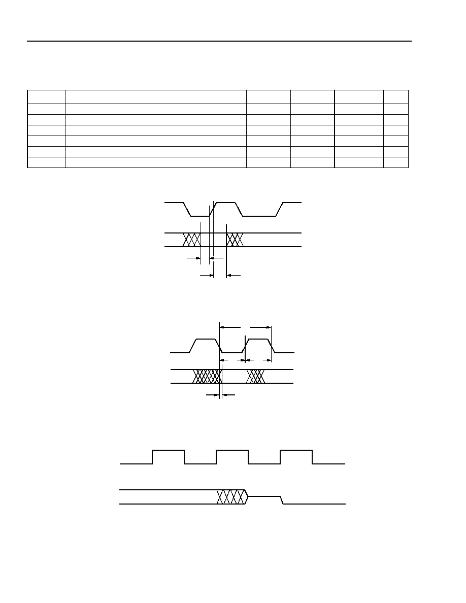
LU3X51FT
Data Sheet
FASTCAT Ethernet Transceiver 10/100Base-TX/FX
July 2000
30
Lucent Technologies Inc.
Timing Characteristics (Preliminary)
Table 26. MII Management Interface Timing (25 pF Load)
* When operating MDC above 6.25 MHz, MDC must be synchronous with LSCLK and have a setup time of 15 ns and a hold time of 5 ns,
with respect to LSCLK.
5-4959(F).a
Figure 5. MDIO Input Timing
5-4960(F).c
Figure 6. MDIO Output Timing
5-5312(F).r1
Note: MDIO turnaround (TA) time is a 2-bit time spacing between the register address field and the data field of a frame to avoid drive conten-
tion on MDIO during a read transaction. During a write to the LU3X51FT, these bits are driven to a 10 by the station. During a read, the
MDIO is not driven during the first bit time and is driven to a 0 by the LU3X51FT during the second bit time.
Figure 7. MDIO During TA (Turnaround) of a Read Transaction
Name
Parameter
Min
Typ
Max
Unit
t1
MDIO Valid to Rising Edge of MDC (setup)
10
--
--
ns
t2
Rising Edge of MDC to MDIO Invalid (hold)
10
--
--
ns
t3
MDC Falling Edge to MDIO Valid (prop. delay)
0
--
40
ns
t4
MDC High*
--
200
--
ns
t5
MDC Low*
40
200
--
ns
t6
MDC Period*
80
400
--
ns
MDC
MDIO
t1
t2
MDC
MDIO
t5
t4
t6
t3
MDC
MDIO
< R >
< Z >
< O >

Lucent Technologies Inc.
31
Data Sheet
LU3X51FT
July 2000
FASTCAT Ethernet Transceiver 10/100Base-TX/FX
Timing Characteristics (Preliminary)
(continued)
Table 27. MII Data Timing (25 pF Load)
* 100 Mbits/s only.
Name
Parameter
Min
Typ
Max
Unit
t1
RXD[3:0], RX_ER, RX_DV Valid to RX_CLK High
10/100
--
--
ns
t2
RX_CLK High to RXD[3:0], RX_DV, RX_ER Invalid
10/100
--
--
ns
t3
RX_CLK High
14/180
--
26/220
ns
t4
RX_CLK Low
14/180
--
26/220
ns
t5
RX_CLK Period
--
40
--
ns
t6
TX_CLK High
14/180
--
26/220
ns
t7
TX_CLK Low
14/180
--
26/220
ns
t8
TX_CLK Period
--
40
--
ns
t9
TXD[3:0], TX_EN, TX_ER, Setup to TX_CLK
15/140
--
--
ns
t10
TXD[3:0], TX_EN, TX_ER, Hold to TX_CLK
0/0
--
--
ns
t11
TXD[3:0], TX_EN, TX_ER Setup to LSCLK*
10
--
--
ns
t12
TXD[3:0], TX_EN, TX_ER, Hold to LSCLK*
0
--
--
ns
t13
First Bit of J on TPIN
Ī
While Transmitting Data to COL
Assert (half-duplex mode)
--
--
170
ns
t14
First Bit of T Received on TPIN
Ī
While Transmitting to COL
Deasserted (half-duplex mode)
--
--
210
ns

LU3X51FT
Data Sheet
FASTCAT Ethernet Transceiver 10/100Base-TX/FX
July 2000
32
Lucent Technologies Inc.
Timing Characteristics (Preliminary)
(continued)
5-5432(F).b
Figure 8. MII Timing Requirements for LU3X51FT
TPIN
Ī
t13
COL
1st BIT OF J
t7
TX_CLK
TXD[3:0]
t6
t8
RX_CLK
RXD[3:0]
t1
t2
TX_EN
t3
t4
t5
RX_DV
RX_ER
TX_ER
t9
t10
LSCLK
TXD[3:0]
t11
TX_EN
TX_ER
t12
1st BIT OF T
t14
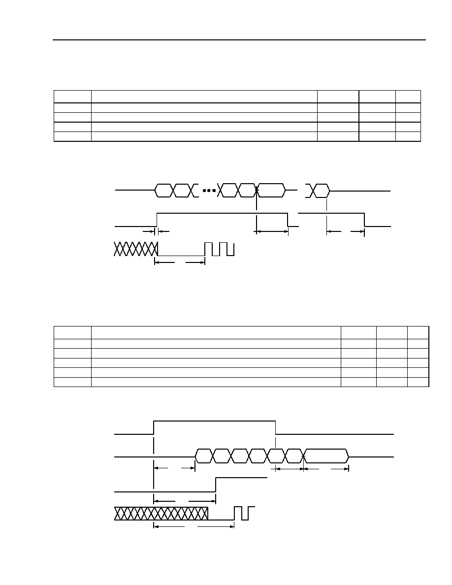
Lucent Technologies Inc.
33
Data Sheet
LU3X51FT
July 2000
FASTCAT Ethernet Transceiver 10/100Base-TX/FX
Timing Characteristics (Preliminary)
(continued)
Table 28. Serial 10 Mbits/s Timing for TPINĪ, CRS, and RX_CLK
5-5293(F).i
Figure 9. Serial 10 Mbits/s Timing for TPINĪ, CRS, and RX_CLK
Table 29. Serial 10 Mbits/s Timing for TX_EN, TPOUTĪ, CRS, and RX_CLK
5-5293(F).j
Figure 10. Serial 10 Mbits/s Timing for TX_EN, TPOUTĪ, CRS, and RX_CLK
Name
Parameter
Min
Max
Unit
t15
TPINĪ Activity to CRS Assertion
40
500
ns
t16
TPINĪ Activity to RX_CLK Valid
800
2300
ns
t17
IDL to CRS Deassertion
200
550
ns
t18
Dead Signal to CRS Deassertion
400
1000
ns
Name
Parameter
Min
Max
Unit
t19
TX_EN Asserted to Transmit Pair Activity
50
400
ns
t20
TX_EN Asserted to CRS Asserted Due to Internal Loopback
5
1900
ns
t21
TX_EN Asserted to RX_CLK Valid Due to Internal Loopback
1000
1700
ns
t22
TX_EN Deasserted to IDL Transmission
50
300
ns
t23
IDL Pulse Width
250
350
ns
TPIN
Ī
CRS
(RECEIVE--START OF PACKET)
(RECEIVE--END OF PACKET)
(RECEIVE--DEAD SIGNAL)
(NOT IDL)
IDL
t15
t17
t16
t18
RX_CLK
TPOUT
Ī
CRS
(TRANSMIT--START OF PACKET)
(TRANSMIT--END OF PACKET)
IDL
t19
t22
t20
t21
t23
TX_EN
RX_CLK
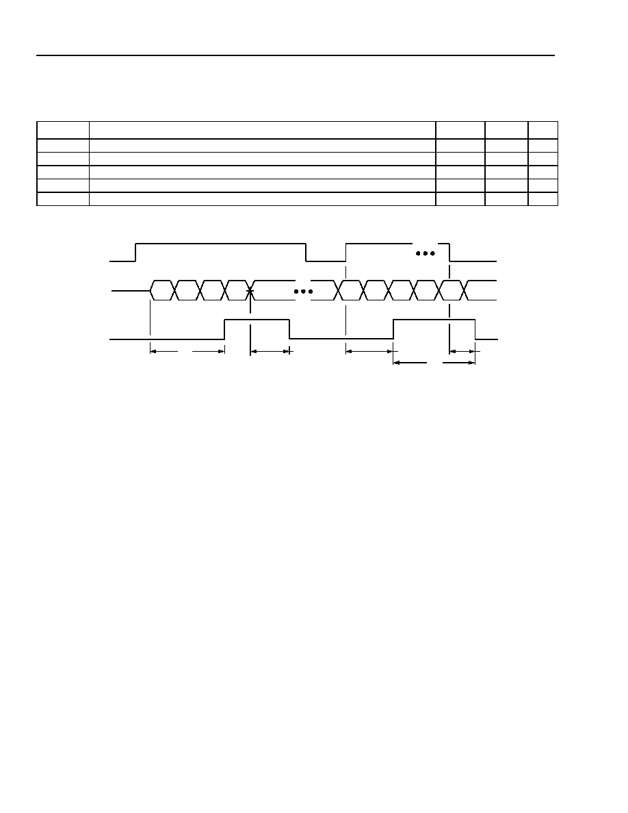
LU3X51FT
Data Sheet
FASTCAT Ethernet Transceiver 10/100Base-TX/FX
July 2000
34
Lucent Technologies Inc.
Timing Characteristics (Preliminary)
(continued)
Table 30. Serial 10 Mbits/s Timing for TX_EN, TPINĪ, and COL
5-5293(F).k
Figure 11. Serial 10 Mbits/s Timing for TX_EN, TPINĪ, and COL
Name
Parameter
Min
Max
Unit
t24
Time to Assert COL; LU3X51FT Is Transmitting; Receive Activity Starts
40
400
ns
t25
Time to Deassert COL; LU3X51FT Is Transmitting; Receive Activity Ceases
300
900
ns
t26
Time to Assert COL; LU3X51FT Is Receiving; Transmit Activity Starts
5
400
ns
t27
Time to Deassert COL; LU3X51FT Is Receiving; Transmit Activity Ceases
5
900
ns
t28
COL Pulse Width
100
--
ns
TPIN
Ī
COL
(TRANSMITTING--RECEIVE COLLISION DETECTED)
(RECEIVING--TRANSMIT COLLISON DETECTED)
IDL
t24
t25
t26
t27
t28
TX_EN
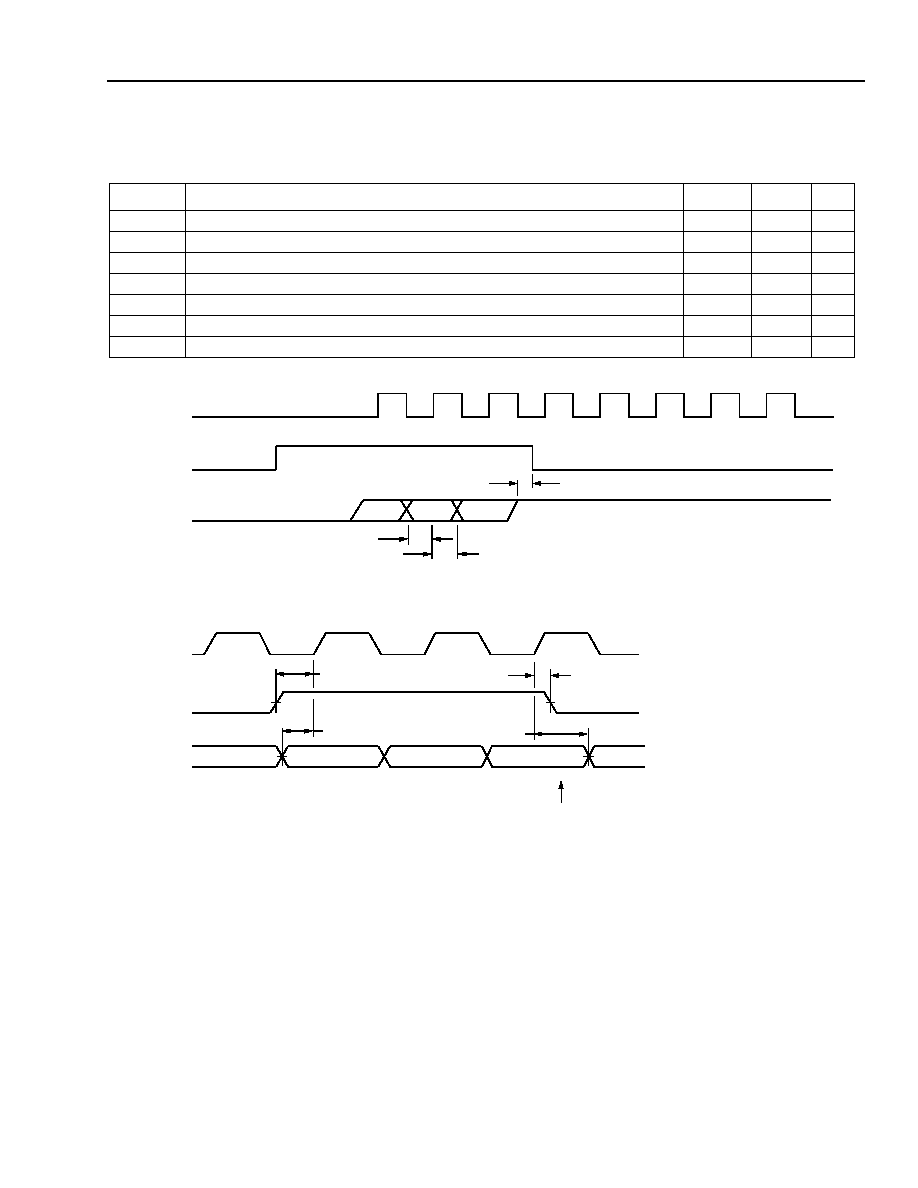
Lucent Technologies Inc.
35
Data Sheet
LU3X51FT
July 2000
FASTCAT Ethernet Transceiver 10/100Base-TX/FX
Timing Characteristics (Preliminary)
(continued)
Table 31. Serial 10 Mbits/s Timing for RX_CLK, CRS, RXD, TX_CLK, TX_EN, and TXD (25 pF Load)
5-2736(F).dr1
Figure 12. Serial 10 Mbits/s Timing for RX_CLK, CRS, RXD, TX_CLK, TX_EN, and TXD
Name
Parameter
Min
Max
Unit
t29
RXD Setup Before RX_CLK Rising Edge
30
--
ns
t30
RXD Held Past RX_CLK Edge
30
--
ns
t31
RX_CLK Low to CRS Deassertion (at end of received packet)
40
--
ns
t32
TX_EN Setup Before TX_CLK Rising Edge
30
--
ns
t33
TX_EN Held Past TX_CLK Rising Edge
0
--
ns
t34
TXD Setup Before TX_CLK Rising Edge
30
--
ns
t35
TXD Held Past TX_CLK Rising Edge
0
--
ns
t31
t30
t29
RX_CLK
CRS
RXD
t32
t34
t33
t35
LAST BIT
TX_CLK
TX_EN
TXD
(START OF PACKET)
(END OF PACKET)
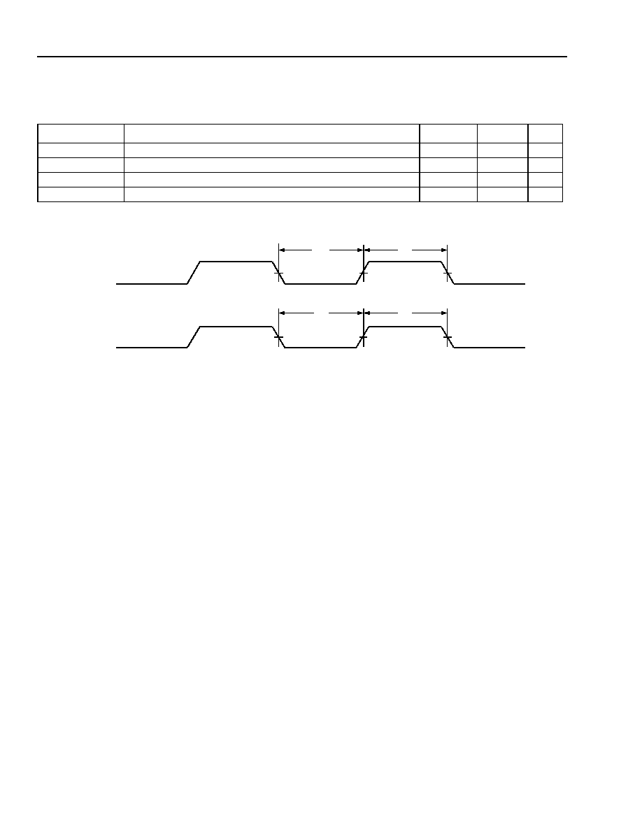
LU3X51FT
Data Sheet
FASTCAT Ethernet Transceiver 10/100Base-TX/FX
July 2000
36
Lucent Technologies Inc.
Timing Characteristics (Preliminary)
(continued)
Table 32. Serial 10 Mbits/s Timing for RX_CLK and TX_CLK (25 pF Load)
5-2737(F).dr1
Figure 13. Serial 10 Mbits/s Timing Diagram for RX_CLK and TX_CLK
Name
Parameter
Min
Max
Unit
t36
RX_CLK Low Pulse Width
45
55
ns
t37
RX_CLK High Pulse Width
45
55
ns
t38
TX_CLK Low Pulse Width
45
55
ns
t39
TX_CLK High Pulse Width
45
55
ns
RX_CLK
TX_CLK
t36
t37
t39
t38
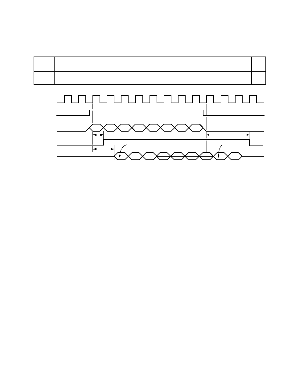
Lucent Technologies Inc.
37
Data Sheet
LU3X51FT
July 2000
FASTCAT Ethernet Transceiver 10/100Base-TX/FX
Timing Characteristics (Preliminary)
(continued)
Table 33. 100 Mbits/s MII Transmit Timing
5-3745(F).d
Figure 14. 100 Mbits/s MII Transmit Timing
Name
Parameter
Min
Max
Unit
t40
Rising Edge of TX_CLK Following TX_EN Assertion to CRS Assertion
--
40
ns
t41
Rising Edge of TX_CLK Following TX_EN Assertion to TPOUT
Ī
--
60
ns
t42
Rising Edge of TX_CLK Following TX_EN Deassertion to CRS Deassertion
--
40
ns
TX_CLK
TX_EN
TXD[3:0]
CRS
TPOUT
Ī
t40
t41
t42
1st BIT OF J
1st BIT OF T

LU3X51FT
Data Sheet
FASTCAT Ethernet Transceiver 10/100Base-TX/FX
July 2000
38
Lucent Technologies Inc.
Timing Characteristics (Preliminary)
(continued)
Table 34. 100 Mbits/s MII Receive Timing
5-3747(F).d
Figure 15. 100 Mbits/s MII Receive Timing
Name
Parameter
Min
Max
Unit
t43
TPIN
Ī
1st Bit of J Receive Activity to CRS Asserted
--
170
ns
t44
TPIN
Ī
Receive Activity to Receive Data Valid
--
210
ns
t45
TPIN
Ī
Receive Activity Cease (1st bit of T) to CRS Deasserted
--
210
ns
t46
TPIN
Ī
Receive Activity Cease (1st bit of T) to Receive Data Not Valid
--
210
ns
TPIN
Ī
t43
t45
t46
CRS
RX_CLK
RX_DV
RX_ER
RXD[3:0]
t44
1st BIT OF J
1st BIT OF T
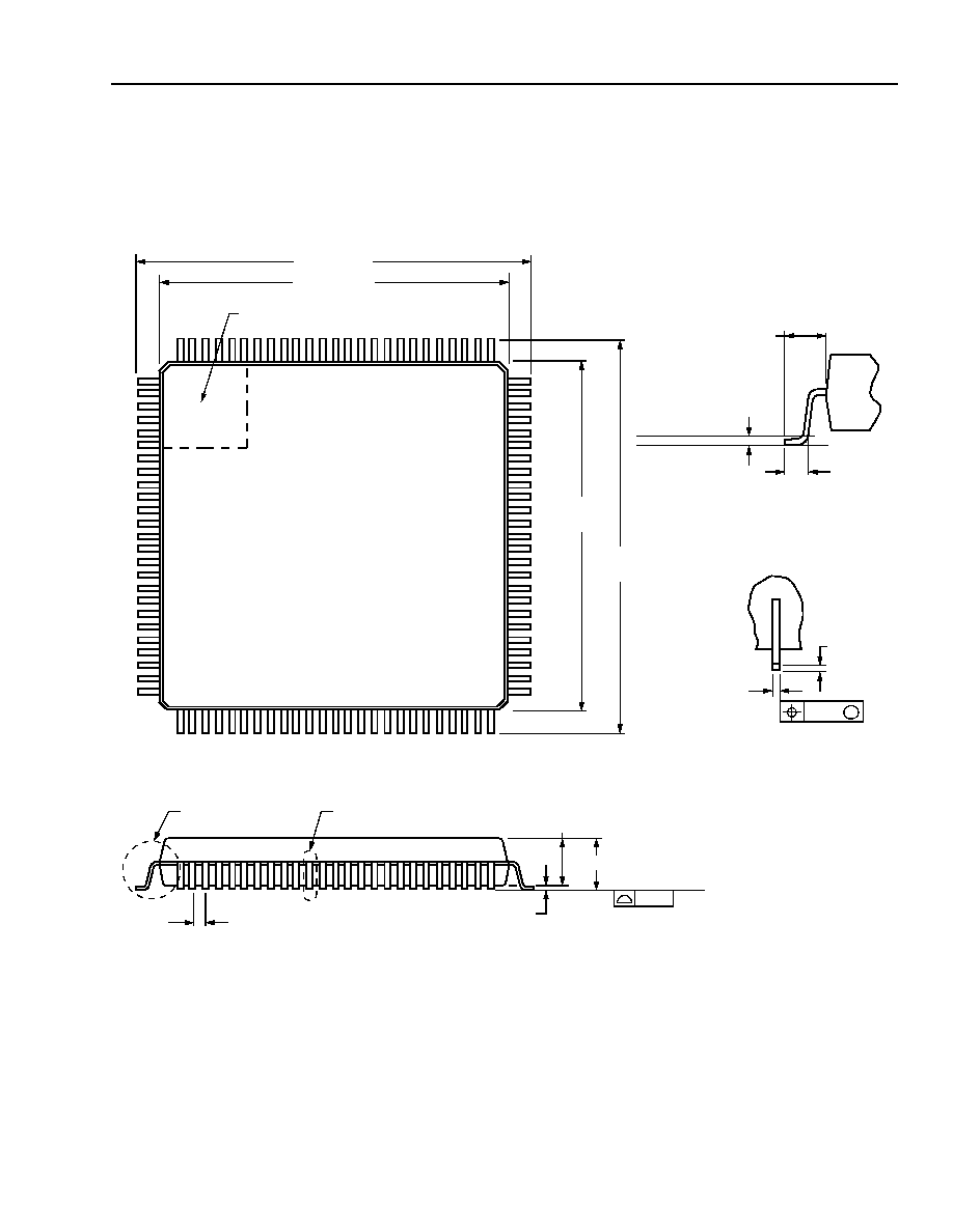
Lucent Technologies Inc.
39
Data Sheet
LU3X51FT
July 2000
FASTCAT Ethernet Transceiver 10/100Base-TX/FX
Outline Diagram
100-Pin TQFP
Dimensions are in millimeters.
5-2146(F).r15
0.50 TYP
1.60 MAX
SEATING PLANE
0.08
1.40 Ī 0.05
0.05/0.15
DETAIL A
DETAIL B
14.00 Ī 0.20
16.00 Ī 0.20
76
100
1
25
26
50
51
75
14.00
Ī 0.20
16.00
Ī 0.20
PIN #1 IDENTIFIER ZONE
DETAIL B
0.19/0.27
0.08
M
0.106/0.200
DETAIL A
0.45/0.75
GAGE PLANE
SEATING PLANE
1.00 REF
0.25

LU3X51FT
Data Sheet
FASTCAT Ethernet Transceiver 10/100Base-TX/FX
July 2000
Lucent Technologies Inc. reserves the right to make changes to the product(s) or information contained herein without notice. N o liability is assumed as a result of their use or application. No
rights under any patent accompany the sale of any such product(s) or information.
FASTCAT is a trademark of Lucent Technologies Inc.
Copyright © 2000 Lucent Technologies Inc.
All Rights Reserved
Printed in U.S.A.
July 2000
DS00-353LAN (replaces DS99-032LAN)
For additional information, contact your Microelectronics Group Account Manager or the following:
INTERNET:
http://www.lucent.com/micro
E-MAIL:
docmaster@micro.lucent.com
N. AMERICA:
Microelectronics Group, Lucent Technologies Inc., 555 Union Boulevard, Room 30L-15P-BA, Allentown, PA 18109-3286
1-800-372-2447, FAX 610-712-4106 (In CANADA: 1-800-553-2448, FAX 610-712-4106)
ASIA PACIFIC: Microelectronics Group, Lucent Technologies Singapore Pte. Ltd., 77 Science Park Drive, #03-18 Cintech III, Singapore 118256
Tel. (65) 778 8833, FAX (65) 777 7495
CHINA:
Microelectronics Group, Lucent Technologies (China) Co., Ltd., A-F2, 23/F, Zao Fong Universe Building, 1800 Zhong Shan Xi Road,
Shanghai 200233 P. R. China Tel. (86) 21 6440 0468, ext. 325, FAX (86) 21 6440 0652
JAPAN:
Microelectronics Group, Lucent Technologies Japan Ltd., 7-18, Higashi-Gotanda 2-chome, Shinagawa-ku, Tokyo 141, Japan
Tel. (81) 3 5421 1600, FAX (81) 3 5421 1700
EUROPE:
Data Requests: MICROELECTRONICS GROUP DATALINE: Tel. (44) 1189 324 299, FAX (44) 1189 328 148
Technical Inquiries: GERMANY: (49) 89 95086 0 (Munich), UNITED KINGDOM: (44) 1344 865 900 (Ascot),
FRANCE: (33) 1 48 83 68 00 (Paris), SWEDEN: (46) 8 600 7070 (Stockholm), FINLAND: (358) 9 4354 2800 (Helsinki),
ITALY: (39) 2 6608131 (Milan), SPAIN: (34) 1 807 1441 (Madrid)
Ordering Information
Device Code
Comcode
Package
Temperature
LU3X51FT-T100-DB
108160623
100-Pin TQFP
0
į
C to 70
į
C