Agilent APDS-9002
Miniature Surface-Mount
Ambient Light Photo Sensor
Data Sheet
Description
The APDS-9002 is a low-cost
analog-output ambient light
photo sensor in lowest cost
miniature chipLED lead-free
surface mount package. It
consists of a spectrally suited
phototransistor, which peaks in
human luminosity curve. Hence,
it provides an excellent
responsivity that is close to the
response of human eyes, as
shown in Figure 2. It provides a
design-alternative to the
HSDL-9000 digital-output
ambient light photo sensor is
suitable for portable
applications with its ultra small
package design.
The APDS-9002 is ideal for
applications in which the
measurement of ambient light is
used to control display back-
lighting. Mobile appliances such
as the mobile phones and PDAs
that draw heavy current from
display backlighting will benefit
from incorporating these photo
sensor products in their designs
by reducing power consumption
significantly.
Features
∑ Excellent responsivity which
peaks in the human luminosity
curve
Close responsivity to the human eye
∑ Miniature chipLED lead-free
surface-mount package
Height ≠ 0.80 mm
Width ≠ 2.00 mm
Depth ≠ 1.25 mm
∑ Good output linearity across wide
illumination range
∑ Low sensitivity variation across
various light sources
∑ Guaranteed temperature
performance
-40
∞
C to 85
∞
C
∑ V
CC
supply 2.4 to 5.5 V
∑ Lead-free package
Applications
∑ Detection of ambient light to
control display backlighting
Mobile devices ≠ mobile phones,
PDAs
Computing devices ≠ notebooks,
webpads
Consumer devices ≠ TVs, video
cameras, digital still cameras
∑ Automatic residential and
commercial lighting management
∑ Electronic signs and signals
∑ Daylight and artificial light
exposed devices

2
Application Support Information
The Application Engineering
Group is available to assist you
with the application design
associated with APDS-9002
ambient light photo sensor
module. You can contact them
through your local sales
representatives for additional
details.
Ordering Information
Part Number
Packaging Type
Package
Quantity
APDS-9002-021
Tape and Reel
4-pins Chipled package
2500
Typical Application Circuit
I/O Pins Configuration Table
Pin
Symbol
Description
1
IOUT
I
OUT
2
VCC
V
CC
3
VCC
V
CC
4
NC
No Connect
Figure 1. Typical application circuit for APDS-9002.
PIN 2: VCC
PIN 3: VCC
APDS-9002
PIN 4: NC
PIN 1: IOUT
RLOAD
Figure 1 Table
Recommended Application
Component
Circuit Components
R
LOAD
1 kW

3
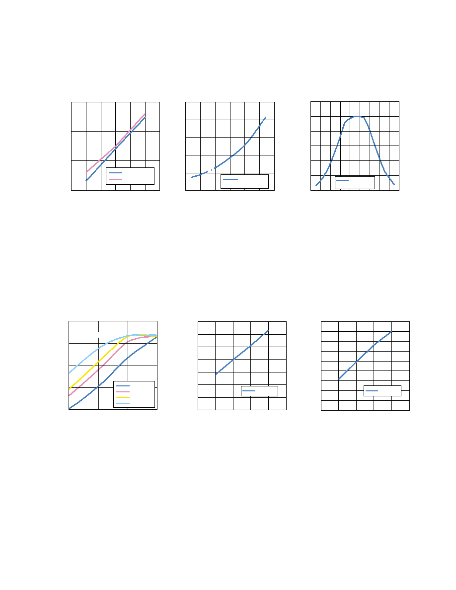
Figure 2. Relative spectral response vs. wavelength.
CAUTIONS: It is advised that normal static precautions be taken in handling and assembly of this
component to prevent damage and/or degradation which may be induced by ESD.
Absolute Maximum Ratings
For implementations where case to ambient thermal resistance is
50
∞
C/W
Parameter
Symbol
Min.
Max.
Units
Storage Temperature
T
S
-40
85
∞
C
Operating Temperature
T
A
-40
85
∞
C
Supply Voltage
V
CC
2.4
5.5
V
Recommended Operating Conditions
Parameter
Symbol
Min.
Max.
Units
Conditions
Operating Temperature
T
A
-40
85
∞
C
Supply Voltage
V
CC
2.4
5.5
V
NORMALIZED RESPONSIVITY
0
WAVELENGTH (nm)
450
0.5
650
0.1
0.4
1.1
1.0
550
1250
1150
1050
950
850
750
350
0.7
0.2
0.3
0.6
0.9
0.8
APDS-9002
SILICON
EYE RESPONSE

4
Electrical & Optical Specifications (T
A
= 25
∞
C)
Parameter
Symbol
Min.
Typ.
Max.
Units
Conditions
Photo Current (I)
I_
PH1
10
20
33
µ
A
V
CC
= 3.0 V, Lux = 10
[2]
Photo Current (II)
I_
PH2
136
250
410
µ
A
V
CC
= 3.0 V, Lux = 100
[2]
Photo Current (III)
I_
PH3
-
300
-
µ
A
V
CC
= 3.0 V, Lux = 100
[1]
Dark Current
I_
DARK
-
50
160
nA
V
CC
= 3.0 V, Lux = 0
Light Current Ratio
I_
PH3
/ I_
PH2
-
1.2
-
-
-
Rise Time
T_
RISE
-
0.95
2
ms
V
CC
= 3.0 V, Lux = 100, R
load
= 1 k
[3]
Fall Time
T_
FALL
-
0.8
2
ms
V
CC
= 3.0 V, Lux = 100, R
load
= 1 k
[3]
Notes:
1. Illuminance by CIE standard light source (incandescent lamp).
2. Fluorescent light is used as light source. White LED is substituted in mass production.
3. White LED is used as light source.
Light Measurement Circuit and Waveforms
R
LOAD
tr
I_pulse
I_pulse
V
OUT
GND
PIN 2: VCC
APDS-9002
PIN 3: VCC
PIN 4: NC
PIN 1: IOUT
tf
90%
10%
5
Figure 3. Photocurrent vs. luminence
(V
CC
= 3 V, T
A
= 25
∞
C).
Figure 4. Normalized photocurrent vs.
temperature (V
CC
= 3 V, 100 LUX).
Figure 5. Normalized photocurrent vs. angle
(V
CC
= 3 V, T
A
= 25
∞
C).
Figure 6. Output voltage vs. luminance at
different load resistor.
Figure 7. Fall time vs. R
LOAD
.
Figure 8. Rise time vs. R
LOAD
.
LUX
PHOTOCURRENT (A)
0.01
0.001
0.0001
0.00001
10
100
1000
Incandescent
Fluorescent
TEMPERATURE (
∞
C)
NORMALIZED PHOTOCURRENT
2.5
1.5
2.0
1.0
0
-50
0
50
100
Normalized
Photocurrent
0.5
ANGLE
NORMALIZED PHOTOCURRENT
1.2
1.0
0
-80 -60 -40 -20
0
20
40
60
80
Normalized
Photocurrent
0.2
0.4
0.6
0.8
RLOAD (W)
FALL TIME (sec)
000.0E+0
200.0E-6
400.0E-6
600.0E-6
800.0E-6
1.0E-3
1.2E-3
1.4E-3
500
0
1000
1500
2000
2500
AVERAGE
RLOAD (W)
Trise (sec)
000.0E+0
200.0E-6
400.0E-6
600.0E-6
800.0E-6
1.0E-3
1.2E-3
1.6E-3
1.4E-3
1.8E-3
500
0
1000
1500
2000
2500
AVERAGE
LUMINANCE, Ev (LUX)
OUTPUT VOLTAGE, V
OUT
(V)
10
1
0.01
0.001
10
100
1000
0.1
R = 1 kW
R = 5.1 kW
R = 11 kW
R = 51 kW
T
A
= 25
∞
C
V
CC
= 3 V
LIGHT SOURCE: WHITE LED