 | ÐлекÑÑоннÑй компоненÑ: AT-42010 | СкаÑаÑÑ:  PDF PDF  ZIP ZIP |
Äîêóìåíòàöèÿ è îïèñàíèÿ www.docs.chipfind.ru
4-154
Up to 6 GHz Medium Power
Silicon Bipolar Transistor
Technical Data
Features
· High Output Power:
12.0 dBm Typical P
1 dB
at 2.0 GHz
20.5 dBm Typical P
1 dB
at 4.0 GHz
· High Gain at
1 dB Compression:
14.0 dB Typical G
1 dB
at 2.0 GHz
9.5 dB Typical G
1 dB
at 4.0 GHz
· Low Noise Figure:
1.9 dB Typical NF
O
at 2.0 GHz
· High Gain-Bandwidth
Product: 8.0 GHz Typical f
T
· Hermetic Gold-ceramic
Microstrip Package
AT-42010
100 mil Package
Description
Hewlett-Packard's AT-42010 is a
general purpose NPN bipolar
transistor that offers excellent
high frequency performance. The
AT-42010 is housed in a hermetic,
high reliability 100 mil ceramic
package. The 4 micron emitter-to-
emitter pitch enables this transis-
tor to be used in many different
functions. The 20 emitter finger
interdigitated geometry yields a
medium sized transistor with
impedances that are easy to match
for low noise and medium power
applications. This device is
designed for use in low noise,
wideband amplifier, mixer and
oscillator applications in the VHF,
UHF, and microwave frequencies.
An optimum noise match near
50
up to 1 GHz , makes this
device easy to use as a low noise
amplifier.
The AT-42010 bipolar transistor is
fabricated using Hewlett-Packard's
10 GHz f
T
Self-Aligned-Transistor
(SAT) process. The die is nitride
passivated for surface protection.
Excellent device uniformity,
performance and reliability are
produced by the use of ion-
implantation, self-alignment
techniques, and gold metalization
in the fabrication of this device.
5965-8910E
4-155
AT-42010 Absolute Maximum Ratings
[1]
Absolute
Symbol
Parameter
Units
Maximum
V
EBO
Emitter-Base Voltage
V
1.5
V
CBO
Collector-Base Voltage
V
20
V
CEO
Collector-Emitter Voltage
V
12
I
C
Collector Current
mA
80
P
T
Power Dissipation
[2,3]
mW
600
T
j
Junction Temperature
°
C
200
T
STG
Storage Temperature
°
C
-65 to 200
Thermal Resistance
[2,4]
:
jc
= 150
°
C/W
Notes:
1. Permanent damage may occur if
any of these limits are exceeded.
2. T
CASE
= 25
°
C.
3. Derate at 6.7 mW/
°
C for
T
C
> 110
°
C.
4. The small spot size of this tech-
nique results in a higher, though
more accurate determination of
jc
than do alternate methods. See
MEASUREMENTS section
"Thermal Resistance" for more
information.
Electrical Specifications, T
A
= 25
°
C
Symbol
Parameters and Test Conditions
[1]
Units Min.
Typ. Max.
|S
21E
|
2
Insertion Power Gain; V
CE
= 8 V, I
C
= 35 mA
f = 2.0 GHz
dB
10.5
11.5
f = 4.0 GHz
5.5
P
1 dB
Power Output @ 1 dB Gain Compression
f = 2.0 GHz
dBm
21.0
V
CE
= 8 V, I
C
= 35 mA
f= 4.0 GHz
20.5
G
1 dB
1 dB Compressed Gain; V
CE
= 8 V, I
C
= 35 mA
f = 2.0 GHz
dB
14.0
f = 4.0 GHz
9.5
NF
O
Optimum Noise Figure: V
CE
= 8 V, I
C
= 10 mA
f = 2.0 GHz
dB
1.9
f = 4.0 GHz
3.0
G
A
Gain @ NF
O
; V
CE
= 8 V, I
C
= 10 mA
f = 2.0 GHz
dB
13.5
f = 4.0 GHz
10.0
f
T
Gain Bandwidth Product: V
CE
= 8 V, I
C
= 35 mA
GHz
8.0
h
FE
Forward Current Transfer Ratio; V
CE
= 8 V, I
C
= 35 mA
--
30
150
270
I
CBO
Collector Cutoff Current; V
CB
= 8 V
µ
A
0.2
I
EBO
Emitter Cutoff Current; V
EB
= 1 V
µ
A
2.0
C
CB
Collector Base Capacitance
[1]
: V
CB
= 8 V, f = 1 MHz
pF
0.28
Notes:
1. For this test, the emitter is grounded.
4-156
AT-42010 Typical Performance, T
A
= 25
°
C
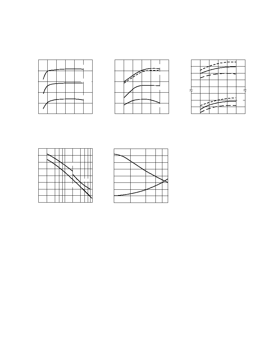
FREQUENCY (GHz)
Figure 4. Insertion Power Gain,
Maximum Available Gain and
Maximum Stable Gain vs. Frequency.
V
CE
= 8 V, I
C
= 35 mA.
GAIN (dB)
0.1
0.5
0.3
1.0
3.0
6.0
I
C
(mA)
Figure 2. Output Power and 1 dB
Compressed Gain vs. Collector
Current and Frequency. V
CE
= 8 V.
24
20
16
12
8
4
G
1 dB
(dB)
P
1 dB
(dBm)
0
10
20
30
40
50
P1dB
G1dB
2.0 GHz
2.0 GHz
4.0 GHz
4.0 GHz
40
35
30
25
20
15
10
5
0
MSG
MAG
|S21E|
2
I
C
(mA)
Figure 1. Insertion Power Gain vs.
Collector Current and Frequency.
V
CE
= 8 V.
20
16
12
8
4
0
|S
21E
|
2
GAIN (dB)
0
10
20
30
40
50
1.0 GHz
2.0 GHz
4.0 GHz
I
C
(mA)
Figure 3. Output Power and 1 dB
Compressed Gain vs. Collector
Current and Voltage. f = 2.0 GHz.
10 V
4 V
6 V
4 V
10 V
6 V
24
20
16
12
16
14
12
10
G
1 dB
(dB)
P
1 dB
(dBm)
0
10
20
30
40
50
P1dB
G1dB
FREQUENCY (GHz)
Figure 5. Noise Figure and Associated
Gain vs. Frequency.
V
CE
= 8 V, I
C
= 10mA.
GAIN (dB)
24
21
18
15
12
9
6
3
0
4
3
2
1
0
NF
O
(dB)
0.5
2.0
1.0
3.0
4.0 5.0
GA
NFO
4-157
AT-42010 Typical Scattering Parameters,
Common Emitter,
Z
O
= 50
, T
A
= 25
°
C, V
CE
= 8 V, I
C
= 10 mA
Freq.
S
11
S
21
S
12
S
22
GHz
Mag.
Ang.
dB
Mag.
Ang.
dB
Mag.
Ang.
Mag.
Ang.
0.1
.74
-47
28.5
26.65
153
-36.4
.015
72
.91
-18
0.5
.65
-136
21.4
11.71
103
-29.4
.034
38
.51
-39
1.0
.63
-168
15.9
6.24
82
-27.2
.044
36
.40
-42
1.5
.63
174
12.6
4.26
69
-26.0
.050
42
.38
-45
2.0
.63
161
10.1
3.23
57
-24.6
.059
43
.38
-49
2.5
.64
154
8.4
2.64
51
-23.0
.070
52
.38
-51
3.0
.65
145
6.9
2.22
41
-22.0
.080
54
.37
-56
3.5
.66
136
5.8
1.94
31
-21.0
.090
51
.38
-65
4.0
.66
126
4.7
1.72
21
-19.7
.104
50
.39
-74
4.5
.66
115
3.8
1.55
11
-18.0
.126
45
.40
-82
5.0
.66
103
3.0
1.41
1
-17.3
.136
41
.40
-89
5.5
.68
90
2.1
1.28
-9
-16.1
.156
36
.40
-98
6.0
.72
81
1.3
1.16
-19
-15.4
.170
31
.37
-110
AT-42010 Typical Scattering Parameters,
Common Emitter, Z
O
= 50
, T
A
= 25
°
C, V
CE
= 8 V, I
C
= 35 mA
Freq.
S
11
S
21
S
12
S
22
GHz
Mag.
Ang.
dB
Mag.
Ang.
dB
Mag.
Ang.
Mag.
Ang.
0.1
.54
-90
33.3
45.97
138
-39.2
.011
54
.76
-29
0.5
.62
-163
22.8
13.83
94
-33.2
.022
52
.34
-40
1.0
.62
177
17.0
7.10
78
-28.8
.036
59
.30
-40
1.5
.62
166
13.6
4.82
67
-26.2
.049
61
.29
-42
2.0
.62
155
11.3
3.65
56
-23.8
.065
57
.29
-47
2.5
.63
150
9.5
2.99
51
-21.8
.081
62
.29
-50
3.0
.64
142
8.0
2.52
42
-21.0
.090
63
.30
-57
3.5
.65
133
6.8
2.19
32
-19.7
.103
59
.30
-67
4.0
.65
124
5.7
1.93
22
-18.4
.120
54
.31
-76
4.5
.65
113
4.7
1.72
13
-17.2
.138
49
.33
-85
5.0
.66
102
3.9
1.56
3
-16.6
.148
45
.34
-92
5.5
.69
91
3.0
1.41
-6
-15.6
.166
39
.33
-100
6.0
.73
83
2.1
1.27
-16
-14.9
.180
32
.30
-110
A model for this device is available in the DEVICE MODELS section.
AT-42010 Noise Parameters:
V
CE
= 8 V, I
C
= 10 mA
Freq.
NF
O
opt
GHz
dB
Mag
Ang
R
N
/50
0.1
1.0
.04
15
0.13
0.5
1.1
.05
76
0.12
1.0
1.5
.10
132
0.12
2.0
1.9
.23
-177
0.11
4.0
3.0
.45
-125
0.26
4-158
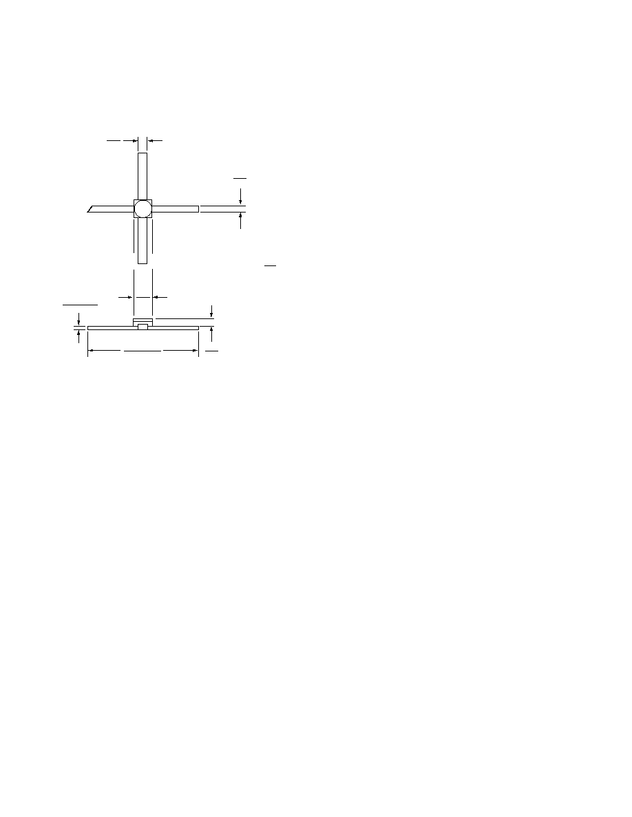
100 mil Package Dimensions
1
3
4
2
EMITTER
EMITTER
COLLECTOR
BASE
.020
.508
.100
2.54
.495
±
.030
12.57
±
.76
Notes:
(unless otherwise specified)
1. Dimensions are in
2. Tolerances
in .xxx =
±
0.005
mm .xx =
±
0.13
mm
.040
1.02
.030
.76
.004
±
.002
.10
±
.05
Document Outline
- List of Figures
- 1. Insertion Power Gain vs. Collector Current and Frequency
- 2. Output Power and 1 dB Compressed Gain vs. Collector Current and Frequency. Vce= 8 V
- 3. Output Power and 1 dB Compressed Gain vs. Collector Current and Frequency. Vce = 8 V
- 4. Insertion Power Gain, Maxiumum Available Gain and Maximum Stable Gain vs. Frequency. Vce = 8, Ic = 35 mA
- 5. Noise Figure and Associated Gain vs. Frequency. Vce= 8 V, Ic=10mA
- Features
- Description
- 100 mil Package
- AT-42010 Absolute Maximum Ratings [1]
- Electrical Specifications, TA = 25°C
- AT-42010 Typical Performance, TA = 25°C
- AT-42010 Typical Scattering Parameters, Common Emitter, ZO = 50 W, TA =25°C, VCE =8 V, ICÊ =Ê 10 mA
- AT-42010 Typical Scattering Parameters, Common Emitter, ZO = 50 W, TA =25°C, VCE =8 V, ICÊ =Ê 35 mA
- AT-42010 Noise Parameters: VCE = 8 V, IC = 10 mA
- 100 mil Package Dimensions