5-23
0.5 ≠ 12 GHz Low Noise
Gallium Arsenide FET
Technical Data
Features
∑ Low Noise Figure:
0.5 dB Typical at 4 GHz
∑ Low Bias:
V
DS
= 2 V, I
DS
= 20 mA
∑ High Associated Gain:
13.0 dB Typical at 4 GHz
∑ High Output Power:
20.0 dBm Typical P
1 dB
at 4 GHz
∑ Cost Effective Ceramic
Microstrip Package
∑ Tape-and Reel Packaging
Option Available
[1]
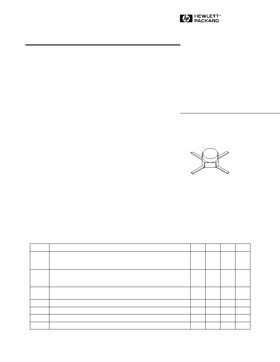
ATF-10136
36 micro-X Package
Electrical Specifications, T
A
= 25
∞
C
Symbol
Parameters and Test Conditions
Units Min.
Typ. Max.
NF
O
Optimum Noise Figure: V
DS
= 2 V, I
DS
= 25 mA
f = 2.0 GHz
dB
0.4
f = 4.0 GHz
dB
0.5
0.6
f = 6.0 GHz
dB
0.8
G
A
Gain @ NF
O
; V
DS
= 2 V, I
DS
= 25 mA
f = 2.0 GHz
dB
16.5
f = 4.0 GHz
dB
12.0
13.0
f = 6.0 GHz
dB
11.0
P
1 dB
Power Output @ 1 dB Gain Compression
f = 4.0 GHz
dBm
20.0
V
DS
= 4 V, I
DS
= 70 mA
G
1 dB
1 dB Compressed Gain: V
DS
= 4 V, I
DS
= 70 mA
f = 4.0 GHz
dB
12.0
g
m
Transconductance: V
DS
= 2 V, V
GS
= 0 V
mmho
70
140
I
DSS
Saturated Drain Current: V
DS
= 2 V, V
GS
= 0 V
mA
70
130
180
V
P
Pinchoff Voltage: V
DS
= 2 V, I
DS
= 1 mA
V
-4.0
-1.3
-0.5
Note:
1. Refer to PACKAGING section "Tape-and-Reel Packaging for Surface Mount Semiconductors."
Description
The ATF-10136 is a high performance
gallium arsenide Schottky-barrier-
gate field effect transistor housed in a
cost effective microstrip package. Its
premium noise figure makes this
device appropriate for use in the first
stage of low noise amplifiers operat-
ing in the 0.5-12 GHz frequency range.
This GaAs FET device has a nominal
0.3 micron gate length using airbridge
interconnects between drain fingers.
Total gate periphery is 500 microns.
Proven gold based metallization
systems and nitride passivation
assure a rugged, reliable device.
5965-8701E

5-24
ATF-10136 Absolute Maximum Ratings
Absolute
Symbol
Parameter
Units
Maximum
[1]
V
DS
Drain-Source Voltage
V
+5
V
GS
Gate-Source Voltage
V
-4
V
GD
Gate-Drain Voltage
V
-7
I
DS
Drain Current
mA
I
DSS
P
T
Power Dissipation
[2,3]
mW
430
T
CH
Channel Temperature
∞
C
175
T
STG
Storage Temperature
[4]
∞
C
-65 to +175
Notes:
1. Permanent damage may occur if
any of these limits are exceeded.
2. T
CASE
TEMPERATURE
= 25
∞
C.
3. Derate at 2.9 mW/
∞
C for
T
CASE
> 25
∞
C.
4. Storage above +150
∞
C may tarnish
the leads of this package making it
difficult to solder into a circuit.
After a device has been soldered
into a circuit, it may be safely
stored up to 175
∞
C.
5. The small spot size of this tech-
nique results in a higher, though
more accurate determination of
jc
than do alternate methods. See
APPLICATIONS PRIMER IIIA for
more information.
ATF-10136 Typical Performance, T
A
= 25
∞
C
Thermal Resistance :
jc
= 350
∞
C/W; T
CH
= 150
∞
C
Liquid Crystal Measurement:
1
µ
m Spot Size
[5]
ATF-10136 Noise Parameters:
V
DS
= 2 V, I
DS
= 25 mA
Freq.
NF
O
opt
GHz
dB
Mag
Ang
R
N
/50
0.5
0.35
0.93
12
0.80
1.0
0.4
0.85
24
0.70
2.0
0.4
0.70
47
0.46
4.0
0.5
0.39
126
0.36
6.0
0.8
0.36
-170
0.12
8.0
1.1
0.45
-100
0.38
Part Number Ordering Information
Part Number
Devices Per Reel
Reel Size
ATF-10136-TR1
1000
7"
ATF-10136-STR
10
STRIP
For more information, see "Tape and Reel Packaging for Semiconductor Devices."
FREQUENCY (GHz)
NF
O
(dB)
I
DS
(mA)
Figure 2. Optimum Noise Figure and
Associated Gain vs. I
DS
.
V
DS
= 2V, f = 4.0 GHz.
NF
O
(dB)
0
20
10
40
50
30
60
Figure 3. Insertion Power Gain,
Maximum Available Gain and
Maximum Stable Gain vs. Frequency.
V
DS
= 2 V, I
DS
= 25 mA.
FREQUENCY (GHz)
GAIN (dB)
2.0
1.5
1.0
0.5
0
18
15
12
9
6
G
A
(dB)
16
14
12
10
G
A
(dB)
2.0
6.0
4.0
8.0 10.0 12.0
1.5
1.0
0.5
0
G
A
G
A
NF
O
NF
O
|S
21
|
2
MSG
MAG
0.5
1.0
2.0
4.0
6.0 8.0 12.0
30
25
20
15
10
5
0
Figure 1. Optimum Noise Figure and
Associated Gain vs. Frequency.
V
DS
= 2V, I
DS
= 25 mA, T
A
= 25
∞
C.
5-25
Typical Scattering Parameters,
Common Source, Z
O
= 50
, T
A
= 25
∞
C, V
DS
= 2 V, I
DS
= 25 mA
Freq.
S
11
S
21
S
12
S
22
MHz
Mag.
Ang.
dB
Mag.
Ang.
dB
Mag.
Ang.
Mag.
Ang.
0.5
.98
-18
14.5
5.32
163
-34.0
.020
78
.35
-9
1.0
.93
-33
14.3
5.19
147
-28.4
.038
67
.36
-19
2.0
.79
-66
13.3
4.64
113
-22.6
.074
59
.30
-31
3.0
.64
-94
12.2
4.07
87
-19.2
.110
44
.27
-42
4.0
.54
-120
11.1
3.60
61
-17.3
.137
31
.22
-49
5.0
.47
-155
10.1
3.20
37
-15.5
.167
13
.16
-54
6.0
.45
162
9.2
2.88
13
-14.3
.193
-2
.08
-17
7.0
.50
120
8.0
2.51
-10
-13.9
.203
-19
.16
45
8.0
.60
87
6.4
2.09
-32
-13.6
.210
-36
.32
48
9.0
.68
61
4.9
1.75
-51
-13.6
.209
-46
.44
38
10.0
.73
42
3.6
1.52
-66
-13.7
.207
-58
.51
34
11.0
.77
26
2.0
1.26
-82
-13.8
.205
-73
.54
27
12.0
.80
14
1.0
1.12
-97
-14.0
.200
-82
.54
15
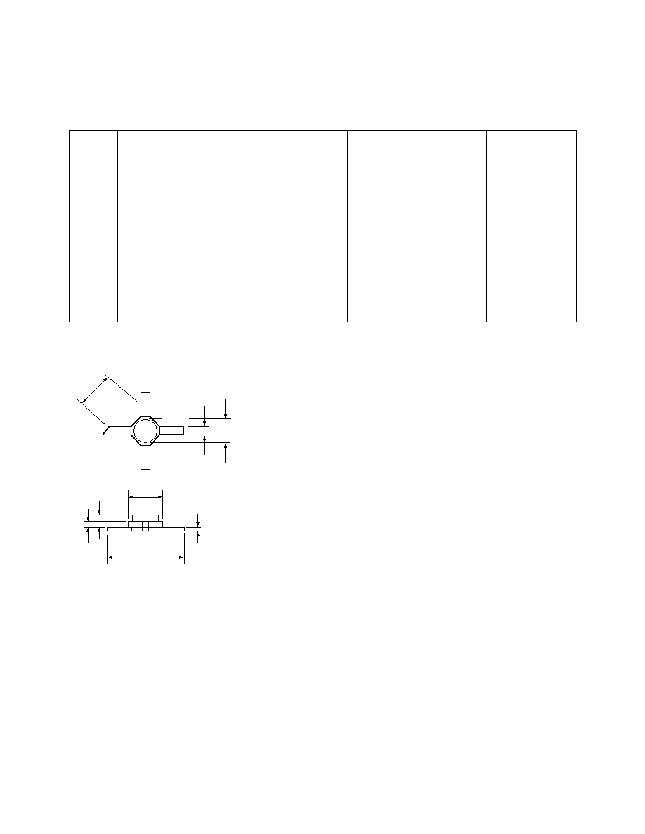
36 micro-X Package
Dimensions
1
3
4
2
SOURCE
SOURCE
DRAIN
GATE
2.15
(0.085)
2.11 (0.083) DIA.
0.508
(0.020)
2.54
(0.100)
4.57
±
0.25
0.180
±
0.010
0.15
±
0.05
(0.006
±
0.002)
Notes:
1. Dimensions are in millimeters (inches)
2. Tolerances: in .xxx =
±
0.005
mm .xx =
±
0.13
0.56
(0.022)
1.45
±
0.25
(0.057
±
0.010)
101