5-36
2 ≠ 16 GHz Low Noise
Gallium Arsenide FET
Technical Data
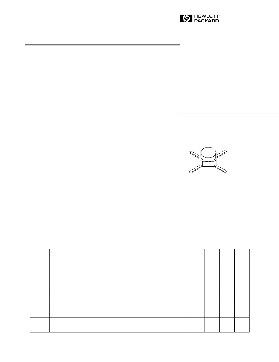
36 micro-X Package
Features
∑ Low Noise Figure:
1.4 dB Typical at 12 GHz
∑ High Associated Gain:
9.0 dB Typical at 12 GHz
∑ High Output Power:
17.5 dBm Typical P
1 dB
at
12 GHz
∑ Cost Effective Ceramic
Microstrip Package
∑ Tape-and-Reel Packaging
Option Available
[1]
Electrical Specifications, T
A
= 25
∞
C
Symbol
Parameters and Test Conditions
Units Min.
Typ. Max.
NF
O
Optimum Noise Figure: V
DS
= 2.5 V, I
DS
= 20 mA
f = 8.0 GHz
dB
1.2
f = 12.0 GHz
dB
1.4
1.6
f = 14.0 GHz
1.6
G
A
Gain @ NF
O
: V
DS
= 2.5 V, I
DS
= 20 mA
f = 8.0 GHz
dB
11.5
f = 12.0 GHz
dB
8.0
9.0
f = 14.0 GHz
dB
7.5
P
1 dB
Power Output @ 1 dB Gain Compression:
f = 12.0 GHz dBm
17.5
V
DS
= 4 V, I
DS
= 40 mA
G
1 dB
1 dB Compressed Gain: V
DS
= 4 V, I
DS
= 40 mA
f = 12.0 GHz
dB
8.5
g
m
Transconductance: V
DS
= 2.5 V, V
GS
= 0 V
mmho
25
55
I
DSS
Saturated Drain Current: V
DS
= 2.5 V, V
GS
= 0 V
mA
40
50
90
V
P
Pinch-off Voltage: V
DS
= 2.5 V, I
DS
= 1 mA
V
-4.0
-1.5
-0.5
Note:
1. Refer to PACKAGING section "Tape-and-Reel Packaging for Surface Mount Semiconductors".
ATF-13336
Description
The ATF-13336 is a high perfor-
mance gallium arsenide Schottky-
barrier-gate field effect transistor
housed in a cost effective micro-
strip package. Its premium noise
figure makes this device appropri-
ate for use in low noise amplifiers
operating in the 2-16 GHz
frequency range.
This GaAs FET device has a
nominal 0.3 micron gate length
with a total gate periphery of
250 microns. Proven gold based
metallization systems and nitride
passivation assure a rugged,
reliable device.
5965-8724E

5-37
ATF-13336 Typical Performance, T
A
= 25
∞
C
ATF-13336 Absolute Maximum Ratings
Absolute
Symbol
Parameter
Units
Maximum
[1]
V
DS
Drain-Source Voltage
V
+5
V
GS
Gate-Source Voltage
V
-4
V
GD
Gate-Drain Voltage
V
-6
I
DS
Drain Current
mA
I
DSS
P
T
Power Dissipation
[2,3]
mW
225
T
CH
Channel Temperature
∞
C
175
T
STG
Storage Temperature
∞
C
-65 to +175
Thermal Resistance :
jc
= 400
∞
C/W; T
CH
= 150
∞
C
Liquid Crystal Measurement:
1
µ
m Spot Size
[5]
Notes:
1. Permanent damage may occur if
any of these limits are exceeded.
2. T
CASE TEMPERATURE
= 25
∞
C.
3. Derate at 2.5mW/
∞
C for
T
CASE
> 85
∞
C.
4. Storage above +150
∞
C may tarnish
the leads of this package difficult to
solder into a circuit. After a device
has been soldered into a circuit, it
may be safely stored up to 175
∞
C.
4. The small spot size of this tech-
nique results in a higher, though
more accurate determination of
jc
than do alternate methods. See
MEASUREMENTS section for
more information.
Part Number Ordering Information
Part Number
Devices Per Reel
Reel Size
ATF-13336-TR1
1000
7"
ATF-13336-STR
10
strip
FREQUENCY (GHz)
NF
O
(dB)
Figure 3. Insertion Power Gain,
Maximum Available Gain and
Maximum Stable Gain vs. Frequency.
V
DS
= 2.5 V, I
DS
= 20 mA.
FREQUENCY (GHz)
GAIN (dB)
2.0
1.5
1.0
0.5
0
16
14
12
10
8
6
G
A
(dB)
6.0
10.0
8.0
12.0 14.0 16.0
GA
NFO
|S21|2
MSG
MAG
2.0
4.0
6.0
8.0 10.0 12.0 16.0
25
20
15
10
5
0
Figure 1. Optimum Noise Figure and
Associated Gain vs. Frequency.
V
DS
= 2.5V, I
DS
= 20 mA, T
A
= 25
∞
C.
I
DS
(mA)
Figure 2. Optimum Noise Figure and
Associated Gain vs. I
DS
.
V
DS
= 2.5V, f = 12.0 GHz.
NF
O
(dB)
0
20
10
40
50
30
60
14
12
10
8
G
A
(dB)
2.5
2.0
1.5
1.0
GA
NFO
ATF-13336 Noise Parameters:
V
DS
= 2.5 V, I
DS
= 20 mA
Freq.
NF
O
opt
GHz
dB
Mag
Ang
R
N
/50
4.0
0.8
.63
93
.27
6.0
1.1
.47
138
.10
8.0
1.2
.40
-153
.20
12.0
1.4
.52
-45
.88
14.0
1.6
.57
-2
1.3
5-38
Typical Scattering Parameters,
Common Emitter, Z
O
= 50
, T
A
= 25
∞
C, V
DS
= 2.5 V, I
DS
= 20 mA
Freq.
S
11
S
21
S
12
S
22
GHz
Mag.
Ang.
dB
Mag.
Ang.
dB
Mag.
Ang.
Mag.
Ang.
2.0
.96
-51
10.6
3.39
127
-27.1
.044
57
.61
-41
3.0
.88
-75
10.3
3.28
106
-23.4
.060
33
.58
-51
4.0
.86
-96
10.1
3.19
86
-22.6
.074
25
.57
-57
5.0
.79
-117
9.9
3.13
66
-20.6
.093
12
.54
-65
6.0
.69
-142
10.2
3.22
46
-18.9
.114
1
.49
-79
7.0
.60
-178
10.1
3.21
21
-17.6
.132
-18
.42
-97
8.0
.54
141
9.8
3.10
-4
-17.3
.137
-33
.31
-112
9.0
.56
103
8.9
2.80
-26
-16.7
.147
-48
.21
-121
10.0
.56
74
8.3
2.60
-48
-16.5
.150
-63
.09
-145
11.0
.58
44
7.6
2.39
-68
-16.8
.145
-78
.07
89
12.0
.63
20
6.7
2.17
-90
-17.5
.133
-95
.16
43
13.0
.65
3
6.0
2.00
-108
-18.3
.121
-107
.19
21
14.0
.66
-7
5.5
1.89
-126
-18.9
.114
-121
.19
-4
15.0
.70
-19
4.9
1.76
-144
-19.0
.112
-129
.16
-28
16.0
.72
-34
4.4
1.66
-175
-19.2
.110
-142
.14
-32
A model for this device is available in the DEVICE MODELS section.
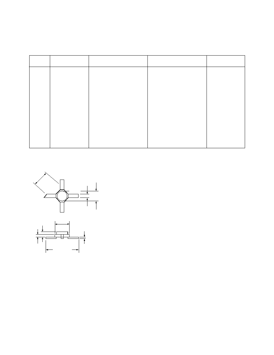
36 micro-X Package Dimensions
1
3
4
2
SOURCE
SOURCE
DRAIN
GATE
2.15
(0.085)
2.11 (0.083) DIA.
0.508
(0.020)
2.54
(0.100)
4.57
±
0.25
0.180
±
0.010
0.15
±
0.05
(0.006
±
0.002)
Notes:
1. Dimensions are in millimeters (inches)
2. Tolerances: in .xxx =
±
0.005
mm .xx =
±
0.13
0.56
(0.022)
1.45
±
0.25
(0.057
±
0.010)
133