
5-63
0.5≠10 GHz General Purpose
Gallium Arsenide FET
Technical Data
ATF-25735
35 micro-X Package
Description
The ATF-25735 is a high perfor-
mance gallium arsenide Schottky-
barrier-gate field effect transistor
housed in a cost effective
Features
∑ High Output Power:
19.0 Bm Typical P
1 dB
at 4 GHz
∑ High Gain:
12.5 dB Typical G
1 dB
at 4 GHz
∑ Low Noise Figure:
1.2 dB Typical at 4 GHz
∑ Cost Effective Ceramic
Microstrip Package
Electrical Specifications, T
A
= 25
∞
C
Symbol
Parameters and Test Conditions
Units Min.
Typ. Max.
NF
O
Optimum Noise Figure: V
DS
= 3 V, I
DS
= 20 mA
f = 2. 0 GHz
dB
1.0
f = 4.0 GHz
1.2
1.5
f = 6.0 GHz
1.4
G
A
Gain @ NF
O
: V
DS
= 3 V, I
DS
= 20 mA
f = 2.0 GHz
dB
15.0
f = 4.0 GHz
11.5
13.0
f =.6.0 GHz
10.5
P
1 dB
Power Output @ 1 dB Gain Compression:
f = 4.0 GHz
dBm
19.0
V
DS
=5 V, I
DS
= 50 mA
G
1 dB
1 dB Compressed Gain: V
DS
= 5 V, I
DS
=50 mA
f = 4.0 GHz
dB
12.5
g
m
Transconductance: V
DS
=3 V, V
GS
= 0 V
mmho
50
80
I
DSS
Saturated Drain Current: V
DS
=3 V, V
GS
= 0 V
mA
50
100
150
V
P
Pinch-off Voltage: V
DS
= 3 V, I
DS
= 1 mA
V
-3.0
-2.0
-0.8
microstrip package. This device is
designed for use in general
purpose amplifier and oscillator
applications in the 0.5-10 GHz
frequency range.
This GaAs FET device has a
nominal 0.3 micron gate length
using airbridge interconnects
between drain fingers. Total gate
periphery is 500 microns. Proven
gold based metallization systems
and nitride passivation assure a
rugged, reliable device.
5965-8710E
5-64
ATF-25735 Typical Performance, T
A
= 25
∞
C
ATF-25735 Absolute Maximum Ratings
Absolute
Symbol
Parameter
Units
Maximum
[1]
V
DS
Drain-Source Voltage
V
+7
V
GS
Gate-Source Voltage
V
-4
V
GD
Gate-Drain Voltage
V
-8
I
DS
Drain Current
mA
I
DSS
P
T
Power Dissipation
[2,3]
mW
450
T
CH
Channel Temperature
∞
C
175
T
STG
Storage Temperature
[4]
∞
C
-65 to +175
Thermal Resistance :
jc
= 325
∞
C/W; T
CH
= 150
∞
C
Liquid Crystal Measurement:
1
µ
m Spot Size
[5[
Notes:
1. Permanent damage may occur if
any of these limits are exceeded.
2. T
CASE TEMPERATURE
= 25
∞
C.
3. Derate at 3 mW/
∞
C for
T
CASE
> 29
∞
C.
4. Storage above +150
∞
C may tarnish
the leads of this package difficult to
solder into a circuit. After a device
has been soldered into a circuit, it
may be safely stored up to 175
∞
C.
5. The small spot size of this tech-
nique results in a higher, though
more accurate determination of
jc
than do alternate methods. See
MEASUREMENTS section for
more information.
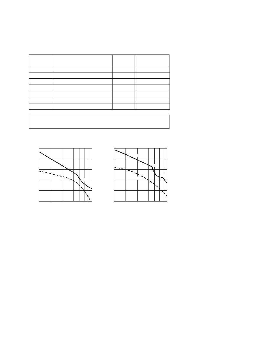
Figure 1. Insertion Power Gain,
Maximum Available Gain and
Maximum Stable Gain vs. Frequency.
V
DS
= 3 V, I
DS
= 20 mA.
Figure 2. Insertion Power Gain,
Maximum Available Gain and
Maximum Stable Gain vs. Frequency.
V
DS
= 5 V, I
DS
= 50 mA.
FREQUENCY (GHz)
GAIN (dB)
|S
21
|
2
MSG
MSG
MAG
0.5
1.0
2.0
4.0 6.0 8.0
12.0
25
20
15
10
5
0
FREQUENCY (GHz)
GAIN (dB)
|S
21
|
2
MSG
MAG
0.5
1.0
2.0
4.0 6.0 8.0
12.0
25
20
15
10
5
0
5-65
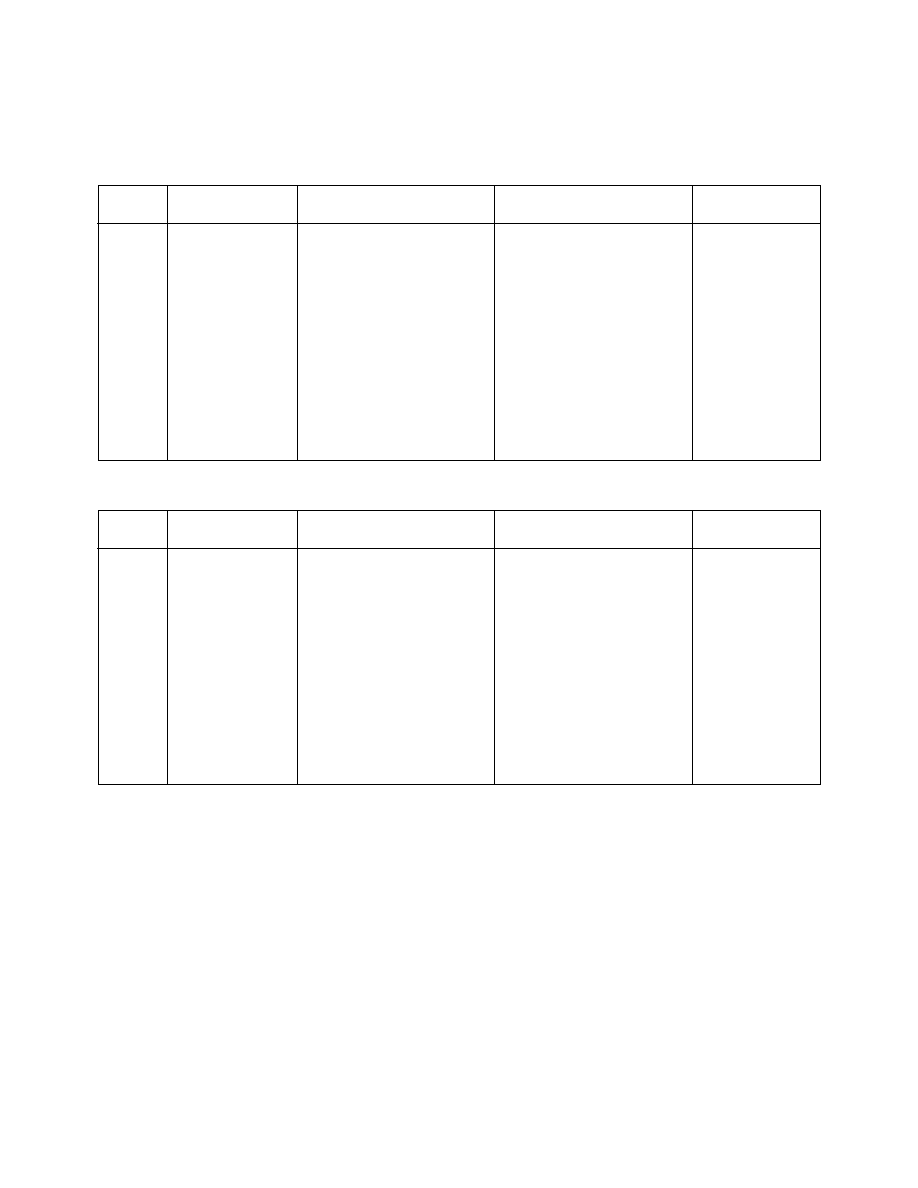
Typical Scattering Parameters,
Common Emitter, Z
O
= 50
, T
A
= 25
∞
C, V
DS
= 3 V, I
DS
= 20 mA
Freq.
S
11
S
21
S
12
S
22
GHz
Mag.
Ang.
dB
Mag.
Ang.
dB
Mag.
Ang.
Mag.
Ang.
0.5
.98
-22
13.9
4.95
159
-32.0
.025
77
.52
-12
1.0
.94
-45
13.3
4.61
142
-27.1
.044
64
.52
-20
2.0
.85
-82
12.2
4.06
110
-21.6
.083
45
.46
-41
3.0
.70
-116
11.0
3.54
81
-19.3
.109
24
.38
-61
4.0
.58
-152
10.0
3.17
54
-17.7
.131
12
.35
-81
5.0
.50
165
8.9
2.78
27
-16.7
.146
-7
.29
-97
6.0
.52
122
7.7
2.43
1
-16.1
.156
-20
.18
-112
7.0
.59
90
6.3
2.06
-23
-15.8
.162
-34
.07
-161
8.0
.65
66
5.1
1.79
-43
-15.5
.167
-46
.09
107
9.0
.69
44
3.8
1.55
-63
-15.3
.172
-53
.15
76
10.0
.73
32
2.7
1.36
-82
-15.4
.170
-65
.18
53
11.0
.79
20
1.1
1.14
-100
-15.5
.168
-78
.21
24
12.0
.84
7
-0.2
.98
-119
-15.7
.161
-93
.26
-5
Typical Scattering Parameters,
Common Emitter, Z
O
= 50
, T
A
= 25
∞
C, V
DS
= 5 V, I
DS
= 50 mA
Freq.
S
11
S
21
S
12
S
22
GHz
Mag.
Ang.
dB
Mag.
Ang.
dB
Mag.
Ang.
Mag.
Ang.
0.5
.93
-21
16.0
6.29
156
-34.0
.020
69
.56
-10
1.0
.88
-42
15.4
5.89
140
-29.6
.033
62
.53
-21
2.0
.78
-81
14.1
5.08
108
-24.4
.060
49
.47
-43
3.0
.65
-112
12.6
4.27
83
-22.6
.074
39
.44
-55
4.0
.55
-142
11.4
3.73
58
-21.0
.089
28
.41
-64
5.0
.48
-176
10.6
3.37
36
-19.7
.104
20
.37
-69
6.0
.47
142
9.7
3.04
10
-18.3
.122
6
.28
-83
7.0
.56
104
8.4
2.64
-14
-17.5
.134
-6
.14
-105
8.0
.65
80
7.0
2.25
-35
-16.7
.146
-17
.07
172
9.0
.73
61
5.8
1.94
-53
-16.1
.157
-26
.14
113
10.0
.78
47
4.7
1.71
-72
-15.4
.169
-40
.20
94
11.0
.80
34
3.6
1.51
-90
-15.1
.176
-53
.27
68
12.0
.85
18
2.7
1.36
-109
-14.8
.181
-64
.36
45
A model for this device is available in the DEVICE MODELS section.

5-66
35 micro-X Package Dimensions
1
3
4
2
SOURCE
DIA.
SOURCE
DRAIN
GATE
.085
2.15
.083
2.11
.020
.508
.100
2.54
.455
±
.030
11.54
±
.76
.006
±
.002
.15
±
.05
Notes:
(unless otherwise specified)
1. Dimensions are in
2. Tolerances
in .xxx =
±
0.005
mm .xx =
±
0.13
mm
.022
.56
.057
±
.010
1.45
±
.25
257