 | –≠–ª–µ–∫—Ç—Ä–æ–Ω–Ω—ã–π –∫–æ–º–ø–æ–Ω–µ–Ω—Ç: ATF-511P8 | –°–∫–∞—á–∞—Ç—å:  PDF PDF  ZIP ZIP |

Agilent ATF-511P8 High Linearity
Enhancement Mode
[1]
Pseudomorphic HEMT in
2x2 mm
2
LPCC
[3]
Package
Data Sheet
Description
Agilent Technologies's
ATF-511P8 is a single-voltage
high linearity, low noise
E-pHEMT housed in an 8-lead
JEDEC-standard leadless
plastic chip carrier (LPCC
[3]
)
package. The device is ideal as
a high linearity, low-noise,
medium-power amplifier. Its
operating frequency range is
from 50 MHz to 6 GHz.
The thermally efficient package
measures only 2 mm x 2 mm x
0.75 mm. Its backside
metalization provides excellent
thermal dissipation as well as
visual evidence of solder reflow.
The device has a Point MTTF of
over 300 years at a mounting
temperature of +85
∞C. All
devices are 100% RF & DC tested.
Features
∑ Single voltage operation
∑ High linearity and P1dB
∑ Low noise figure
∑ Excellent uniformity in product
specifications
∑ Small package size:
2.0 x 2.0 x 0.75 mm
∑ Point MTTF > 300 years
[2]
∑ MSL-1 and lead-free
∑ Tape-and-reel packaging option
available
Specifications
2 GHz; 4.5V, 200 mA (Typ.)
∑ 41.7 dBm output IP3
∑ 30 dBm output power at 1 dB gain
compression
∑ 1.4 dB noise figure
∑ 14.8 dB gain
∑ 12.1 dB LFOM
[4]
∑ 69% PAE
Applications
∑ Front-end LNA Q2 and Q3 driver or
pre-driver amplifier for Cellular/
PCS and WCDMA wireless
infrastructure
∑ Driver amplifier for WLAN,
WLL/RLL and MMDS applications
∑ General purpose discrete E-pHEMT
for other high linearity applications
Pin Connections and
Package Marking
Note:
Package marking provides orientation and
identification:
"1P" = Device Code
"x" = Date code indicates the month of
manufacture.
Note:
1. Enhancement mode technology employs a
single positive V
gs
, eliminating the need of
negative gate voltage associated with
conventional depletion mode devices.
2. Refer to reliability datasheet for detailed
MTTF data.
3. Conforms to JEDEC reference outline MO229
for DRP-N.
4. Linearity Figure of Merit (LFOM) is essentially
OIP3 divided by DC bias power.
Pin 1 (Source)
Pin 2 (Gate)
Pin 3
Pin 4 (Source)
Pin 8
Pin 7 (Drain)
Pin 6
Pin 5
1Px
Top View
Pin 8
Source
(Thermal/RF Gnd)
Pin 7 (Drain)
Pin 6
Pin 5
Pin 1 (Source)
Pin 2 (Gate)
Pin 3
Pin 4 (Source)
Bottom View
2
ATF-511P8 Absolute Maximum Ratings
[1]
Absolute
Symbol
Parameter
Units
Maximum
V
DS
Drain≠Source Voltage
[2]
V
7
V
GS
Gate≠Source Voltage
[2]
V
-5 to 1
V
GD
Gate Drain Voltage
[2]
V
-5 to 1
I
DS
Drain Current
[2]
A
1
I
GS
Gate Current
mA
46
P
diss
Total Power Dissipation
[3]
W
3
P
in max.
RF Input Power
[4]
dBm
+30
T
CH
Channel Temperature
∞C
150
T
STG
Storage Temperature
∞C
-65 to 150
ch_b
Thermal Resistance
[5]
∞C/W
33
Notes:
1. Operation of this device in excess of any one
of these parameters may cause permanent
damage.
2. Assumes DC quiescent conditions.
3. Board (package belly) temperatureT
B
is 25
∞C.
Derate 30 mW/
∞C for T
B
> 50
∞C.
4. With 10 Ohm series resistor in gate supply
and 3:1 VSWR.
5. Channel-to-board thermal resistance
measured using 150
∞C Liquid Crystal
Measurement method.
6. Device can safely handle +30dBm RF Input
Power provided IGS limited to 46mA. IGS at
P1dB drive level is bias circuit dependent.
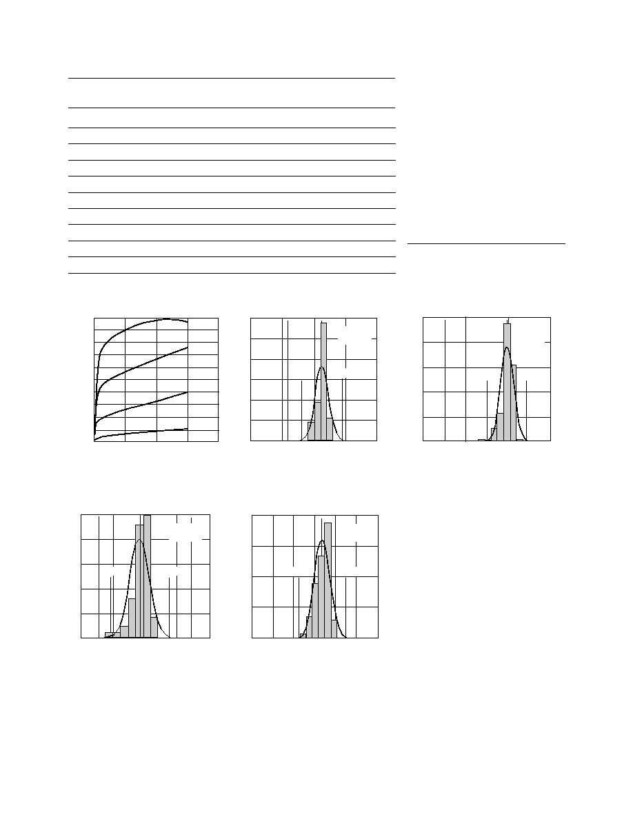
Product Consistency Distribution Charts at 2 GHz, 4.5V, 200 mA
[6,7]
OIP3 (dBm)
Figure 2. OIP3
LSL = 38.5, Nominal = 41.7.
35
41
38
44
47
240
200
160
120
80
40
0
Cpk = 1.66
Stdev = 0.6
-3 Std
+3 Std
P1dB (dBm)
Figure 3. P1dB
LSL = 28.5, Nominal = 30.
28
30
29
31
200
160
120
80
40
0
Cpk = 3.24
Stdev = 0.15
-3 Std
+3 Std
GAIN (dB)
Figure 4. Gain
LSL = 13.5, Nominal = 14.8, USL = 16.5.
13
15
14
16
17
150
120
90
60
30
0
Cpk = 1.4
Stdev = 0.31
-3 Std
+3 Std
Notes:
6. Distribution data sample size is 400 samples taken from 4 different wafers and 3 different lots.
Future wafers allocated to this product may have nominal values anywhere between the upper and
lower limits.
7. Measurements are made on production test board, which represents a trade-off between optimal
OIP3, P1dB and VSWR. Circuit losses have been de-embedded from actual measurements.
Figure 1. Typical I-V Curves
(Vgs = 0.1 per step).
V
DS
(V)
1000
900
800
700
600
500
400
300
200
100
0
0
2
4
6
8
I
DS
(mA)
0.8 V
0.7 V
0.5 V
0.6 V
PAE (%)
Figure 5. PAE
LSL = 52, Nominal = 68.9.
52
62
57
67
72
77
82
160
120
80
40
0
Cpk = 3.03
Stdev = 1.85
-3 Std
+3 Std

3
ATF-511P8 Electrical Specifications
T
A
= 25
∞C, DC bias for RF parameters is Vds = 4.5V and Ids = 200 mA unless otherwise specified.
Symbol
Parameter and Test Condition
Units
Min.
Typ.
Max.
Vgs
Operational Gate Voltage
Vds = 4.5V, Ids = 200 mA
V
0.25
0.51
0.8
Vth
Threshold Voltage
Vds = 4.5V, Ids = 32 mA
V
--
0.28
--
Idss
Saturated Drain Current
Vds = 4.5V, Vgs = 0V
µA
--
16.4
--
Gm
Transconductance
Vds = 4.5V, Gm =
Idss/Vgs;
mmho
--
2178
--
Vgs = Vgs1 ≠ Vgs2
Vgs1 = 0.55V, Vgs2 = 0.5V
Igss
Gate Leakage Current
Vds = 0V, Vgs = -4.5V
µA
-27
-2
--
NF
Noise Figure
[1]
f = 2 GHz
dB
--
1.4
--
f = 900 MHz
dB
--
1.2
--
G
Gain
[1]
f = 2 GHz
dB
13.5
14.8
16.5
f = 900 MHz
dB
--
17.8
--
OIP3
Output 3
rd
Order Intercept Point
[1,2]
f = 2 GHz
dBm
38.5
41.7
--
f = 900 MHz
dBm
--
43
--
P1dB
Output 1dB Compressed
[1]
f = 2 GHz
dBm
28.5
30
--
f = 900 MHz
dBm
--
29.6
--
PAE
Power Added Efficiency
f = 2 GHz
%
52
68.9
--
f = 900 MHz
%
--
68.6
--
ACLR
Adjacent Channel Leakage
Offset BW = 5 MHz
dBc
--
-58.9
--
Power Ratio
[1,3]
Offset BW = 10 MHz
dBc
--
-62.7
--
Notes:
1. Measurements obtained using production test board described in Figure 6 and PAE tested at P1dB condition.
2. I ) 2 GHz OIP3 test condition: F1 = 2.0 GHz, F2 = 2.01 GHz and Pin = -5 dBm per tone.
II ) 900 MHz OIP3 test condition: F1 = 900 MHz, F2 = 910 MHz and Pin = -5 dBm per tone.
3. ACLR test spec is based on 3GPP TS 25.141 V5.3.1 (2002-06)
- Test Model 1
- Active Channels: PCCPCH + SCH + CPICH + PICH + SCCPCH + 64 DPCH (SF=128)
- Freq = 2140 MHz
- Pin = -5 dBm
- Channel Integrate Bandwidth = 3.84 MHz
4. Use proper bias, board, heatsink and derating designs to ensure maximum channel temperature is not exceeded. See absolute maximum ratings and
application note for more details.
Input
50 Ohm
Transmission
Line and
Gate Bias T
(0.3 dB loss)
Input
Matching Circuit
_mag = 0.69
_ang = -164∞
(1.1 dB loss)
Output
Matching Circuit
_mag = 0.65
_ang = -163∞
(0.9 dB loss)
DUT
50 Ohm
Transmission
Line and
Drain Bias T
(0.3 dB loss)
Output
Figure 6. Block diagram of the 2 GHz production test board used for NF, Gain, OIP3 , P1dB and PAE and ACLR measurements. This circuit achieves a
trade-off between optimal OIP3, P1dB and VSWR. Circuit losses have been de-embedded from actual measurements.

4
Gamma Load and Source at Optimum OIP3 and P1dB Tuning Conditions
The device's optimum OIP3 and P1dB measurements were determined using a load pull system at 4.5V,
200 mA quiesent bias:
Figure 7. Simplified schematic of production test board. Primary purpose is to show 15 Ohm series resistor placement in
gate supply. Transmission line tapers, tee intersections, bias lines and parasitic values are not shown.
RF Input
1.2 pF
1.2 pF
2.7 nH
1.8 nH
RF Output
50 Ohm
.02
110 Ohm
.03
110 Ohm
.03
50 Ohm
.02
DUT
15 nH
15 Ohm
2.2
µF
Gate
DC Supply
47 nH
2.2
µF
Drain
DC Supply
Optimum OIP3
Freq
Gamma Source
Gamma Load
OIP3
Gain
P1dB
PAE
(GHz)
Mag
Ang
Mag
Ang
(dBm)
(dB)
(dBm)
(%)
0.9
0.776
152
0.549
-178
43.3
17.94
29.63
63.8
2.0
0.872
-171
0.683
-179
43.1
15.06
30.12
66.8
2.4
0.893
-162
0.715
-174
42.8
14.03
29.90
64.5
3.9
0.765
-132
0.574
-144
41.7
9.47
29.02
52
Optimum P1dB
Freq
Gamma Source
Gamma Load
OIP3
Gain
P1dB
PAE
(GHz)
Mag
Ang
Mag
Ang
(dBm)
(dB)
(dBm)
(%)
0.9
0.773
153
0.784
-173
38.0
19.28
31.9
54.23
2.0
0.691
147
0.841
-166
36.4
10.34
31.4
38.15
2.4
0.797
164
0.827
-166
36.2
8.43
31.2
37.38
3.9
0.602
-163
0.794
-155
35.4
7.03
31
32.72
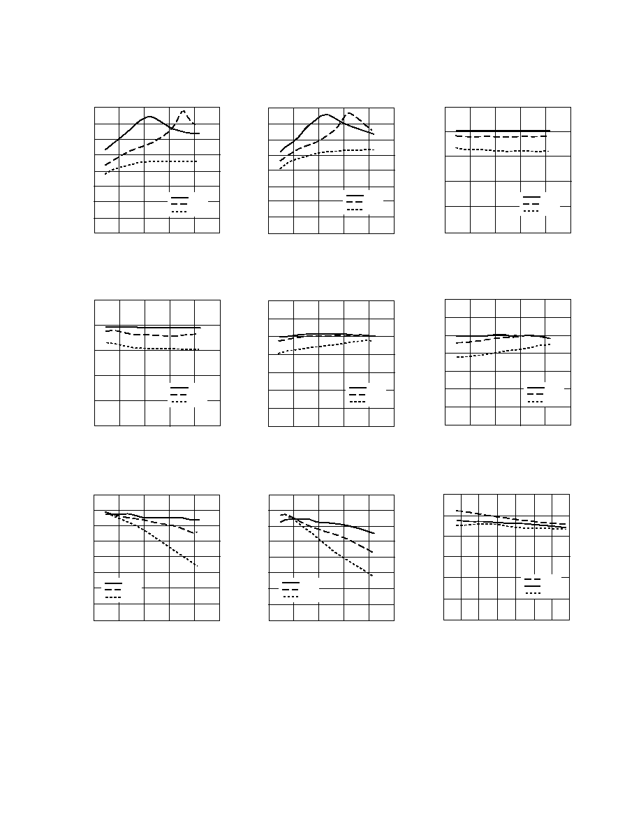
5
ATF-511P8 Typical Performance Curves (at 25
∞C unless specified otherwise)
Tuned for Optimal OIP3 at 4.5V 200 mA
Note:
Bias current for the above charts are quiescent
conditions. Actual level may increase or
decrease depending on amount of RF drive.
IDS (mA)
Figure 8. OIP3 vs. I
DS
and V
DS
at 2 GHz.
OIP3 (dBm)
50
50
45
40
35
30
25
20
15
10
550
150
350
450
250
4.5 V
4 V
3 V
IDS (mA)
Figure 9. OIP3 vs. I
DS
and V
DS
at 900 MHz.
OIP3 (dBm)
50
50
45
40
35
30
25
20
15
10
550
150
350
450
250
4.5 V
4 V
3 V
Idq (mA)
Figure 10. P1dB vs. I
dq
and V
DS
at 2 GHz.
P1dB (dBm)
50
35
30
25
20
15
10
550
150
350
450
250
4.5 V
4 V
3 V
Idq (mA)
Figure 11. P1dB vs.
Idq
and V
DS
at 900 MHz.
P1dB (dBm)
50
35
30
25
20
15
10
550
150
350
450
250
4.5 V
4 V
3 V
IDS (mA)
Figure 12. Gain vs. I
DS
and V
DS
at 2 GHz.
GAIN (dB)
50
17
16
15
14
13
12
11
10
550
150
350
450
250
4.5 V
4 V
3 V
IDS (mA)
Figure 13. Gain vs. I
DS
and V
DS
at 900 MHz.
GAIN (dB)
50
20
19
18
17
16
15
14
13
550
150
350
450
250
4.5 V
4 V
3 V
Idq (mA)
Figure 14. PAE vs. I
dq
and V
DS
at 2 GHz.
PAE (%)
50
80
70
60
50
40
30
20
10
0
550
150
350
450
250
4.5 V
4 V
3 V
Idq (mA)
Figure 15. PAE vs. I
dq
and V
DS
at 900 MHz.
PAE (%)
50
80
70
60
50
40
30
20
10
0
550
150
350
450
250
4.5 V
4 V
3 V
FREQUENCY (GHz)
Figure 16. OIP3 vs. Temp and Freq.
OIP3 (dBm)
0.5
50
45
40
35
30
25
20
4
1
2
2.5
1.5
3
3.5
-40
∞C
25
∞C
85
∞C