 | –≠–ª–µ–∫—Ç—Ä–æ–Ω–Ω—ã–π –∫–æ–º–ø–æ–Ω–µ–Ω—Ç: HDCP-2010 | –°–∫–∞—á–∞—Ç—å:  PDF PDF  ZIP ZIP |
Agilent HDCP-2010
Image Processor
Data Sheet
Description
The HDCP-2010 provides a
complete image-processing
pipeline for the Agilent family of
CMOS image sensors. This part
transforms the raw output data
from the CMOS sensor into final
images using a high performance
image processor. Complete
sensor control is performed by
the HDCP-2010, including auto-
exposure, illumination compen-
sation, and auto white balance.
Data output is 4:4:4 or 4:2:2 YUV
or compressed JPEG via parallel
or serial interface.
The HDCP-2010 enables imaging
in many different types of
devices, such as handheld
computers, cellular phones, and
notebook computers. The chip-
set combination of the HDCP-
2010 and a HDCS CMOS image
sensor delivers to another device
a complete image in JPEG
format, ready for storage or
transmission. By producing a
high-quality finished picture, the
host system is relieved of all
image-processing, thus allowing
for the incorporation of imaging
technology in a wide range of
products.
For standalone imaging, the
HDCP-2010 can be coupled with
a low-cost micro-controller to
provide a complete camera
solution. The HDCP-2010 con-
tains the entire image processing
system, while the micro-control-
ler controls the image storage,
user interface and power man-
agement. The simple system
designs enabled by the HDCP-
2010 will bring imaging to new
product types and markets.
Features
∑ High quality image processor --
sophisticated imaging algorithms
∑ Fully processed image output --
Direct JPEG or YUV format
∑ Auto-exposure
∑ Auto white balance
∑ Pixel correction
∑ Versatile image pipeline -- fully
programmable gamma correction
and color balance matrices
∑ Demosaic
∑ Color space conversion
∑ Pixel processing rate-- 12 million
pixels/second
∑ Reference design and evaluation
kit available-- includes USB VGA
camera, PC drivers/software, and
schematics
Sensors Supported
∑ HDCS-1020 (CIF)
∑ HDCS-2020 (VGA)
Applications
∑ PDAs
∑ Notebook computers
∑ Video phones
∑ Low-cost digital still cameras

2
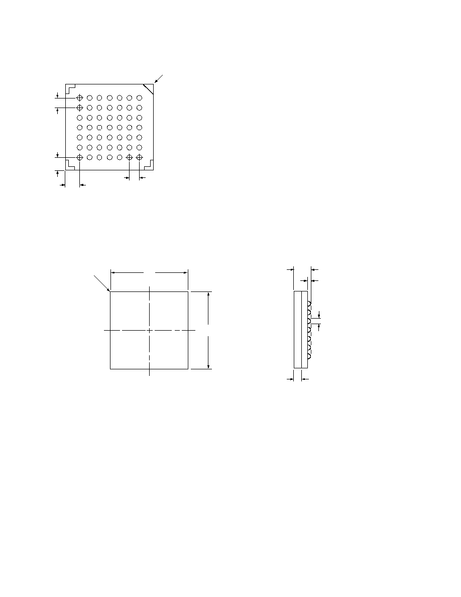
Package Ball Layout
The HDCP-2010 uses a 49 ball ChipArray TM.
7
6
5
4
3
2
1
A
B
C
D
E
F
G
Figure 1. Ball Grid Array (bottom view).
Table 1. Package Pin Assignment and Function.
Pin
Name
Type
Pin
Name
Type
A1
IPC_TWIN_sdata
Input/output
D5
Gnd
Ground
A2
Mode_select[0]
Input
D6
GPIO_0
Input/output
A3
IPC_TWIN_sclk
Input
D7
Vdd_3.3V
Power
A4
Sensor_clock
Output
E1
End_of_frame
Output
A5
Sensor_nRow
Input
E2
End_of_line
Output
A6
Sensor_data_ready
Input
E3
Data_ready
Output
A7
Sensor_nReset
Output
E4
Data_output[0]
Output
B1
Mode_select [1]
Input
E5
Sensor_data[0]
Input
B2
Mode_select [2]
Input
E6
Sensor_data[1]
Input
B3
Reserve/NO CONNECT
Output
E7
Sensor_data[3]
Input
B4
GPIO_1
Input/output
F1
Data_output[3]
Output
B5
nPOR
Input
F2
Data_output[1]
Output
B6
Sensor_TWIN_data
Input/output
F3
Data_output[2]
Output
B7
Sensor_nFrame
Input
F4
Sensor_data[2]
Input
C1
VddA_1.8V
Power
F5
Sensor_data[4]
Input
C2
Vdd_1.8V
Power
F6
Sensor_data[6]
Input
C3
Crystal_output
output
F7
Sensor_data[5]
Input
C4
Gnd
Ground
G1
Data_output[7]
Output
C5
Gnd
Ground
G2
Data_output[5]
Output
C6
Vdd_1.8V
Power
G3
Data_output[4]
Output
C7
Sensor_TWIN_clock
Output
G4
Data_output[6]
Output
D1
Gnd
Ground
G5
Sensor_data[8]
Input
D2
Crystal_input
Input
G6
Sensor_data[9]
Input
D3
Vdd_3.3V
Power
G7
Sensor_data[7]
Input
D4
Gnd
Ground

3
Pin Descriptions
Power and Ground
Table 2. Power and Ground Pin Numbers and Descriptions.
Pin Name
Pin
Type
Function
Vdd_1.8V
C2, C6
Power
Core Vdd input ≠ 1.8V nominal
VddA_1.8V
C1
Power
Analog Vdd input ≠ 1.8V nominal
Vdd_3.3V
D3, D7
Power
Pad Vdd input ≠ 3.3V nominal
Gnd
C4, C5, D1, D4, D5
Ground
Ground connection
Miscellaneous
Table 3. Mode Select, Clock, General Purpose Input/Output and Reset Pin Numbers and Descriptions.
Pin Name
Pin
Type
Function
Mode_select[0]
A2
Input
Determine clock mode and place HDCP-2010 in suspend/low power mode.
Mode_select[1]
B1
Input
See Table 3.
Mode_select[2]
B2
Input
Crystal_output
C3
Input/output
16 MHz crystal output in normal mode.
Crystal_input
D2
Input
16 MHz crystal or external clock connection in normal mode. Connect to the same
clock (48 MHz) signal as Crystal_output when operating in external mode.
GPIO_0
D6
Input/output
General-purpose input/output connection. Controlled through GPIO register.
GPIO_1
B4
Input/output
General-purpose input/output connection. Controlled through GPIO register.
nPOR
B5
Input
Active low power on reset connection (hold for 100 msec during power on).
Table 4. Clocking and Suspend/Low Power Modes.
Input Logic Level
Mode
Description
Mode_select[2]
Mode_select[1]
Mode_select[0]
Normal
Use crystal/external clock plus internal PLL
0
0
0
External
Use external clock and bypass internal PLL
0
1
1
Tri-state
Tri-state all pads
1
1
0
Two Wire Serial Interface
Table 5. Two Wire Serial Interface (TWIN) Pin Numbers and Descriptions.
Pin Name
Pin
Type
Function
IPC_TWIN_sclk
A3
Input
Receive serial data transfer synchronization signal (SCLK) from a master device.
IPC_TWIN_sdata
A1
Input/output
Send/receive serial data signal (SDATA).

4
Pin Descriptions,
continued
HDCP-2010 Image Data Output
Table 6. Image Data Output Pin Numbers and Descriptions.
Pin Name
Pin
Type
Function
Data_ready
E3
Output
Transmit Data_ready signal when in parallel output mode. In serial output mode,
Data_ready provides a serial synchronization signal.
End_of_line
E2
Output
Transmit End_of_line signal indicating that an image row has been transmitted
when in parallel mode. In serial mode, End_of_line signals data valid.
End_of_frame
E1
Output
Transmit End_of_frame signal indicating last byte of frame and between frame
states in both parallel and serial modes.
Data_output[0]
E4
Output
Output 8-bit parallel data in parallel mode. In serial mode, Data_output[7] transmits
Data_output[1]
F2
Output
serialized data stream.
Data_output[2]
F3
Output
Data_output[3]
F1
Output
Data_output[4]
G3
Output
Data_output[5]
G2
Output
Data_output[6]
G4
Output
Data_output[7]
G1
Output
Agilent CMOS Sensor Interface
Table 7. Image Sensor Interface Pin Numbers and Descriptions.
Pin Name
Pin
Type
Function
Sensor_clock
A4
Output
Provide system clock signal to image sensor.
Sensor_nReset
A7
Output
Transmit initialization signal to image sensor.
Sensor_TWIN_clock
C7
Output
Transmit serial data transfer synchronization signal.
Sensor_TWIN_data
B6
Input/output
Serial data transmission. This line is used to configure and monitor the sensor.
Sensor_data_ready
A6
Input
Receive data ready signal from image sensor.
Sensor_nRow
A5
Input
Receive signal indicating that an image row has been transmitted.
Sensor_nFrame
B7
Input
Receive signal indicating that an entire image frame has been transmitted.
Sensor_data[0]
E5
Input
Receive parallel digitized pixel data from the image sensor.
Sensor_data[1]
E6
Input
Sensor_data[2]
F4
Input
Sensor_data[3]
E7
Input
Sensor_data[4]
F5
Input
Sensor_data[5]
F7
Input
Sensor_data[6]
F6
Input
Sensor_data[7]
G7
Input
Sensor_data[8]
G5
Input
Sensor_data[9]
G6
Input
5
7
6
5
4
3
2
1
A
B
C
D
E
F
G
A1 Ball Pad Corner
0.80
1.10
REF
1.10 REF
Bottom View: 49 solder balls
0.80
Title????
Package Dimensions
A1 Ball Pad Corner
7.00
7.00
Top View
Side View
0.36
±
0.05
1.40
±
0.10
0.70
±
0.05
0.46 TYP