 | –≠–ª–µ–∫—Ç—Ä–æ–Ω–Ω—ã–π –∫–æ–º–ø–æ–Ω–µ–Ω—Ç: HDMP-0440 | –°–∫–∞—á–∞—Ç—å:  PDF PDF  ZIP ZIP |
Agilent HDMP-0440
Quad Port Bypass Circuit
for Fibre Channel Arbitrated Loops
Data Sheet
Features
∑ Supports 1.0625 GBd Fibre
Channel operation
∑ Supports 1.25 GBd Gigabit
Ethernet (GE) operation
∑ Quad PBC in one package
∑ Equalizers on all inputs
∑ High-speed LVPECL I/O
∑ Buffered Line Logic (BLL) outputs
(no external bias resistors
required)
∑ 0.5 W typical power at V
CC
= 3.3 V
∑ 44 Pin, 10 mm, low-cost plastic
QFP package
Applications
∑ RAID, JBOD, BTS cabinets
∑ Two 2:1 muxes
∑ Two 1:2 buffers
∑ 1
N Gigabit serial buffer
∑ N
1 Gigabit serial mux
Description
The HDMP-0440 is a Quad Port
Bypass Circuit (PBC), which
provides a low-cost, low-power
physical-layer solution for Fibre
Channel Arbitrated Loop (FC-AL)
disk array configurations. By using
a PBC such as the HDMP-0440,
hard disks may be pulled out or
swapped while other disks in the
array are available to the system.
A PBC consists of multiple 2:1
multiplexers daisy chained
together. Each port has two modes
of operation: "disk in loop" and
"disk bypassed." When the "disk in
loop" mode is selected, the loop
goes into and out of the disk drive
at that port. For example, data goes
from the HDMP-0440's
TO_NODE[n]
±
differential output
pins to the Disk Drive Transceiver
IC's (e.g. an HDMP-1636A) Rx
differential input pins. Data from
the Disk Drive Transceiver IC's Tx
differential outputs goes to the
HDMP-0440's FM_NODE[n]
±
differential input pins. Figure 2
shows connection diagrams for
disk drive array applications.
When the "disk bypassed" mode
is selected, the disk drive is either
absent or non-functional and the
loop bypasses the hard disk.
The "disk bypassed" mode is
enabled by pulling the
BYPASS[n]- pin low. Leave
BYPASS[n]- floating to enable the
"disk in loop" mode. HDMP-
0440s may be cascaded with
other members of the HDMP-
04XX/HDMP-05XX family
through the appropriate
FM_NODE[n]
±
and
TO_NODE[n]
±
pins to
accommodate any number of
hard disks (see Figure 3). The
unused cells in the HDMP-0440
may be bypassed by using
pulldown resistors on the
BYPASS[n]- pins for these cells.
An HDMP-0440 may also be
configured as five 1:1 buffers, as
two 2:1 multiplexers or as two
1:2 buffers.
CAUTION: As with all semiconductor ICs, it is advised that normal static precautionsb be taken in
the handling and assembly of this component to prevent damage and/or degradation which may be
induced by electrostatic discharge (ESD).
HDMP-0440

2
HDMP-0440 Block Diagram
BLL OUTPUT
All TO_NODE[n]
±
high-speed
differential outputs are driven by
a Buffered Line Logic (BLL)
circuit that has on-chip source
termination, so no external bias
resistors are required. The BLL
Outputs on the HDMP-0440 are
of equal strength and can drive
lengthy FR-4 PCB trace.
Unused outputs should not be left
unconnected. Ideally, unused
outputs should have their
differential pins shorted together
with a short PCB trace. If longer
traces or transmission lines are
connected to the output pins, the
lines should be differentially
terminated with an appropriate
resistor. The value of the
termination resistor should match
the PCB trace differential
impedance.
EQU INPUT
All FM_NODE[n]
±
high-speed
differential inputs have an
Equalization (EQU) buffer to
offset the effects of skin loss and
dispersion on PCBs. An external
termination resistor is required
across all high-speed inputs. The
value of the termination resistor
should match the PCB trace
differential impedance.
Alternatively, instead of a single
resistor, two resistors in series,
with an AC ground between them,
can be connected differentially
across the FM_NODE[n]
±
inputs.
The latter configuration
attenuates high-frequency
common mode noise.
BYPASS[n]- INPUT
The active low BYPASS[n]- inputs
control the data flow through the
HDMP-0440. All BYPASS pins are
LVTTL and contain internal pull-
up circuitry. To bypass a port,
the appropriate BYPASS[n]- pin
should be connected to GND
through a 1 k
resistor.
Otherwise, the BYPASS[n]- inputs
should be left to float, as the
internal pull-up circuitry will
force them high.
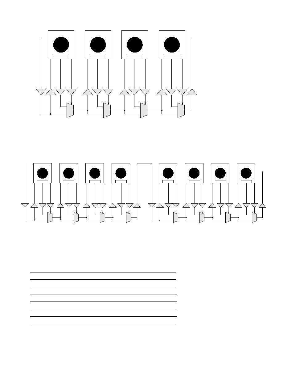
Figure 1. Block diagram of HDMP-0440.
FM_NODE[1]
TO_NODE[1]
BYPASS[1]≠
1
0
TO_NODE[0]
FM_NODE[2]
TO_NODE[2]
1
0
FM_NODE[3]
TO_NODE[3]
1
0
FM_NODE[4]
TO_NODE[4]
1
0
BLL
EQU
TTL
BYPASS[2]≠
BLL
EQU
TTL
BYPASS[3]≠
BLL
EQU
TTL
BYPASS[4]≠
BLL
EQU
TTL
BLL
FM_NODE[0]
EQU
3
Figure 2. Connection diagram for disk array applications.
Figure 3. Connection diagram for multiple HDMP-0440s.
I/O Type Definitions
I/O Type
Definition
I-LVTTL
LVTTL Input
O-LVTTL
LVTTL Output
HS_OUT
High Speed Output, LVPECL compatible
HS_IN
High Speed Input
C
External Circuit Node
S
Power Supply or Ground
FM_NODE[1]
TO_NODE[1]
BYPASS[1]≠
1
0
TO_NODE[0] = TO_LOOP
FM_NODE[2]
TO_NODE[2]
1
0
FM_NODE[3]
TO_NODE[3]
1
0
FM_NODE[4]
TO_NODE[4]
1
0
BLL
EQU
TTL
BYPASS[2]≠
BLL
EQU
TTL
BYPASS[3]≠
BLL
EQU
TTL
BYPASS[4]≠
BLL
EQU
TTL
BLL
FM_NODE[0] = FM_LOOP
EQU
SERDES
HARD DISK A
HARD DISK B
HARD DISK C
HARD DISK D
SERDES
SERDES
SERDES
1
2
3
4
TO_NODE[1]
FM_NODE[1]
BYPASS[1]≠
1
0
SERDES
HARD DISK A
TO_NODE[0]
1
TO_NODE[2]
FM_NODE[2]
BYPASS[2]≠
1
0
2
TO_NODE[3]
FM_NODE[3]
BYPASS[3]≠
1
0
3
TO_NODE[4]
FM_NODE[4]
BYPASS[4]≠
1
0
4
HARD DISK B
HARD DISK C
HARD DISK D
SERDES
SERDES
SERDES
BLL
EQU
TTL
BLL
EQU
TTL
BLL
EQU
TTL
BLL
EQU
TTL
BLL
TO_NODE[0] = TO_LOOP
FM_NODE[0]
1
0
TO_NODE[4]
FM_NODE[4]
BYPASS[4]
4
TO_NODE[1]
FM_NODE[1]
BYPASS[1]≠
1
0
1
TO_NODE[2]
FM_NODE[2]
BYPASS[2]≠
1
0
2
TO_NODE[3]
FM_NODE[3]
BYPASS[3]≠
1
0
3
HARD DISK H
HARD DISK E
HARD DISK F
SERDES
SERDES
SERDES
BLL
EQU
BLL
EQU
TTL
BLL
EQU
TTL
BLL
EQU
TTL
BLL
EQU
TTL
HARD DISK G
SERDES
FM_NODE[0] = FM_LOOP
EQU

4
Pin Definitions
Pin Name
Pin
Pin Type
Pin Description
TO_NODE[0]+
24
HS_OUT
Serial Data Outputs: High-speed outputs to a hard disk drive or to a cable.
TO_NODE[0]-
25
TO_NODE[1]+
07
TO_NODE[1]-
06
TO_NODE[2]+
44
TO_NODE[2]-
43
TO_NODE[3]+
38
TO_NODE[3]-
37
TO_NODE[4]+
31
TO_NODE[4]-
30
FM_NODE[0]+
10
HS_IN
Serial Data Inputs: High-speed inputs from a hard disk drive or from a cable.
FM_NODE[0]-
09
FM_NODE[1]+
04
FM_NODE[1]-
03
FM_NODE[2]+
41
FM_NODE[2]-
40
FM_NODE[3]+
35
FM_NODE[3]-
34
FM_NODE[4]+
28
FM_NODE[4]-
27
BYPASS[0]-
14
I-LVTTL
Bypass Inputs: For "disk bypassed" mode, connect BYPASS[n]- to GND
BYPASS[1]-
15
through a 1 k
resistor. For "disk in loop" mode, float HIGH.
BYPASS[2]-
16
BYPASS[3]-
17
BYPASS[4]-
18
GND
01
S
Ground: Normally 0 V. See Figure 9 for Recommended Power Supply Filtering.
08
11
12
13
19
22
23
33
39
V
CC
HS[0]
26
S
High Speed Supply: Normally 3.3 V. Used only for high-speed outputs(
V
CC
HS[1]
05
S
TO_NODE[n]). See Figure 9 for Recommended Power Supply Filtering.
V
CC
HS[2]
42
S
V
CC
HS[3]
36
S
V
CC
HS[4]
29
S
V
CC
02
S
Logic Power Supply: Normally 3.3 V. Used for internal logic. See Figure 9 for
14
Recommended Power Supply Filtering.
20
21
32

5
Absolute Maximum Ratings
T
A
= 25
∞
C, except as specified. Operation in excess of any of these conditions may result in permanent damage to this
device. Continuous operation at these minimum or maximum ratings is not recommended.
Symbol
Parameter
Units
Min.
Max.
V
CC
Supply Voltage
V
≠0.5
4.0
V
IN,LVTTL
LVTTL Input Voltage
V
≠0.5
V
CC
+ 0.5
[1]
V
IN,HS_IN
HS_IN Input Voltage (Differential)
mV
200
2000
I
O,LVTTL
LVTTL Output Sink/Source Current
mA
±
13
T
stg
Storage Temperature
∞
C
≠65
+150
T
j
Junction Temperature
∞
C
0
+125
Note:
1. Must remain less than or equal to absolute maximum V
CC
voltage of 4.0 V.
DC Electrical Specifications
T
A
= 0
∞
C to +70
∞
C, V
CC
= 3.15 V to 3.45 V.
Symbol
Parameter
Units
Min.
Typ.
Max.
V
IH,LVTTL
LVTTL Input High Voltage Range
V
2.0
V
IL,LVTTL
LVTTL Input Low Voltage Range
V
0.8
V
OH,LVTTL
LVTTL Output High Voltage Range, I
OH
= -400
µ
A
V
2.2
V
CC
V
OL,LVTTL
LVTTL Output Low Voltage Level, I
OL
= 1 mA
V
0
0.6
I
IH,LVTTL
Input High Current (Magnitude), V
IN
= 2.4 V, V
CC
= 3.45 V
µ
A
40
I
IL,LVTTL
Input Low Current (Magnitude), V
IN
= 0.4 V, V
CC
= 3.45 V
µ
A
≠600
I
CC
Total Supply Current, T
A
= 25
∞
C
mA
150
185