 | –≠–ª–µ–∫—Ç—Ä–æ–Ω–Ω—ã–π –∫–æ–º–ø–æ–Ω–µ–Ω—Ç: HEDS-1500 | –°–∫–∞—á–∞—Ç—å:  PDF PDF  ZIP ZIP |
Features
∑ Focused Emitter and
Detector in a Single Package
∑ 655 nm Visible Emitter
∑ 0.178 mm (0.007) Resolution
∑ TO-5 Miniature Sealed
Package
∑ Photodiode Output
Description
The HEDS-1500 is a fully inte-
grated module designed for
applications requiring optical
reflective sensing. The module
contains a 655 nm visible LED
HEDS-1500
655 nm Precision Optical
Reflective Sensor
Technical Data
emitter and a matched I.C. photo-
detector. A bifurcated aspheric
lens is used to image the active
areas of the emitter and the
detector to a single spot 4.27 mm
(0.168 in.) in front of the pack-
age. The output signal is a current
generated by the photodiode.
Applications
Applications for the HEDS-1500
include bar code scanning,
pattern recognition and verifica-
tion, object sizing, optical limit
switching, tachometry, textile
thread counting and defect
detection, dimensional monitor-
ing, line locating, paper edge
detection, and any application
where precision optical reflective
sensing is desired.
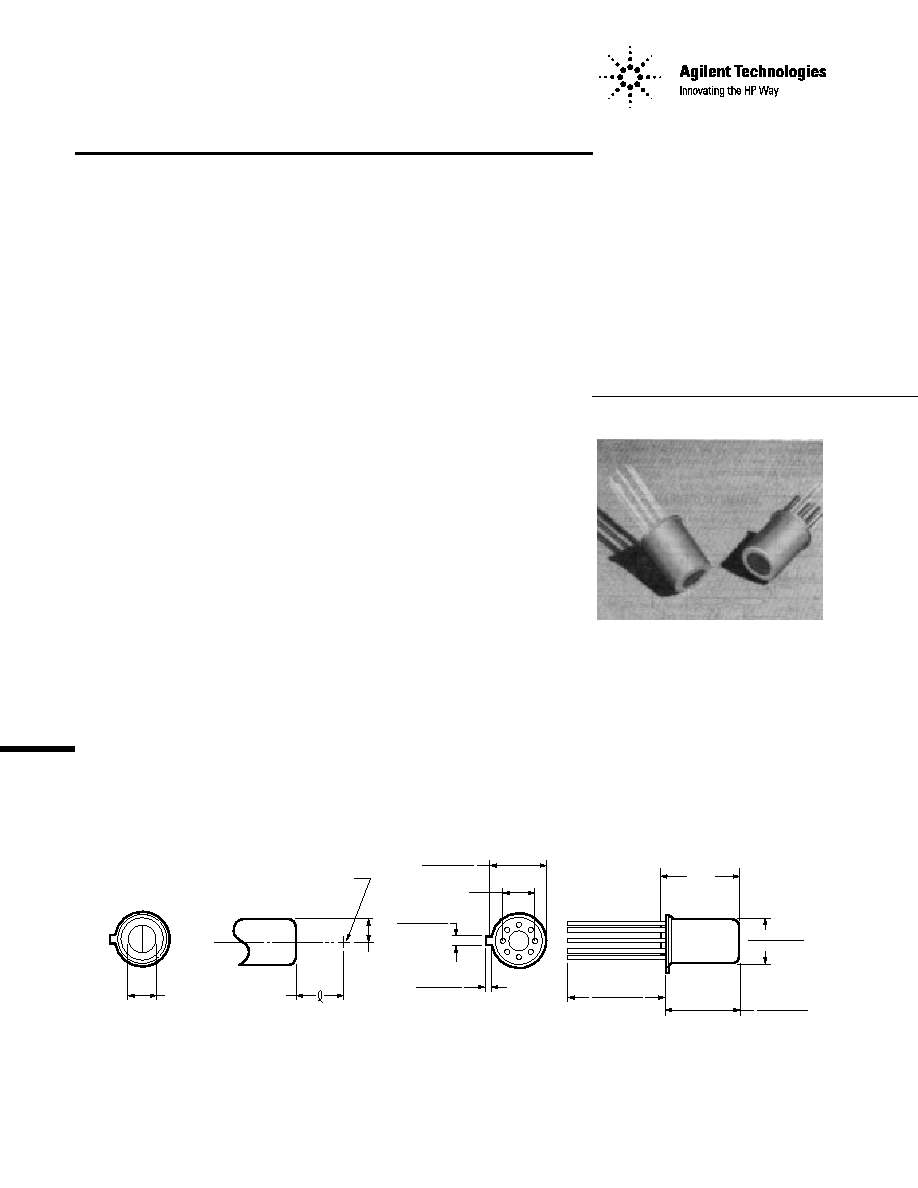
Mechanical
Considerations
The HEDS-1500 is packaged in a
high profile 8 pin TO-5 metal can
with a glass window. The emitter
and photodetector chips are
mounted on the header at the
base of the package. Positioned
above these active elements is a
CL
5.08
(0.200)
REFERENCE PLANE
MAXIMUM SIGNAL POINT
4.27 ± 0.25
(0.168 ± 0.010)
5.08
(0.200)
9.40 (0.370)
8.51 (0.335)
0.86 (0.034)
0.73 (0.029)
1.14 (0.045)
0.73 (0.029)
15.24 (0.600)
12.70 (0.500)
11.50 (0.453)
11.22 (0.442)
8.33 (0.328)
7.79 (0.307)
12.0
(0.473)
S.P.
R.P.
NOTES:
1. ALL DIMENSIONS IN MILLIMETERS AND (INCHES).
2. ALL UNTOLERANCED DIMENSIONS ARE FOR REFERENCE ONLY.
3. THE REFERENCE PLANE (R.P.) IS THE TOP SURFACE OF THE PACKAGE.
4. NICKEL CAN AND GOLD PLATED LEADS.
5. S.P. = SEATING PLANE.
6. THE LEAD DIAMETER IS 0.45 mm (0.018 IN.) TYP.
4.11
(0.162)
Package Dimensions
2
bifurcated aspheric acrylic lens
that focuses them to the same
point.
The sensors can be rigidly se-
cured by commercially available
two piece TO-5 style heat sinks,
such as Thermalloy 2205, Aavid
Engineering 321527, or 8 pin
0.200 inch diameter pin circle
sockets. These fixtures provide a
stable reference platform for
affixing the HEDS-1500 to a
circuit board.
In applications requiring contact
scanning, protective focusing tips
are available. Focusing tips are
available in either metal or poly-
carbonate packages using a
sapphire ball as the contact
surface. The Agilent part numbers
are HEDS-3001, HBCS-2999,
HBCS-4999, HBCS-A998, and
HBCS-A999.
Electrical Operation
The detector of the sensor is a
single photodiode. Figure 7 shows
photocurrent being supplied from
the cathode of the photodiode to
an inverting input of the opera-
tional amplifier. The cathode of
the 655 nm emitter is physically
and electrically connected to the
case-substrate of the device.
Applications that require modula-
tion or switching of the LED
should be designed to have the
cathode connected to the electri-
cal ground of the system.
Applications where ambient light
is present will require a special
LED drive and recovery circuit to
achieve the full resolution of the
sensor. Application Note 1040
provides data and schematics to
support HEDS-1500 sensor oper-
ation in ambient light conditions.
A reliability data sheet is available
for the HEDS-1500 precision
optical reflective sensor.
Absolute Maximum Ratings @ T
A
= 25
∞
C
Parameter
Symbol
Min.
Max.
Units
Note
Operating Temperature
T
A
-20
70
∞
C
Storage Temperature
T
S
-40
75
∞
C
Lead Soldering Temperature
260
∞
C
1
for 10 sec.
Average LED Forward Current
I
f
50
mA
Peak LED Forward Current
I
fp
(data pending)
2
Reverse LED Input Voltage
V
r
5
V
Photodiode Bias (-V = forward bias)
V
d
-0.3
7
V
3
(See next page for Notes.)
7
3
5
2
6
4
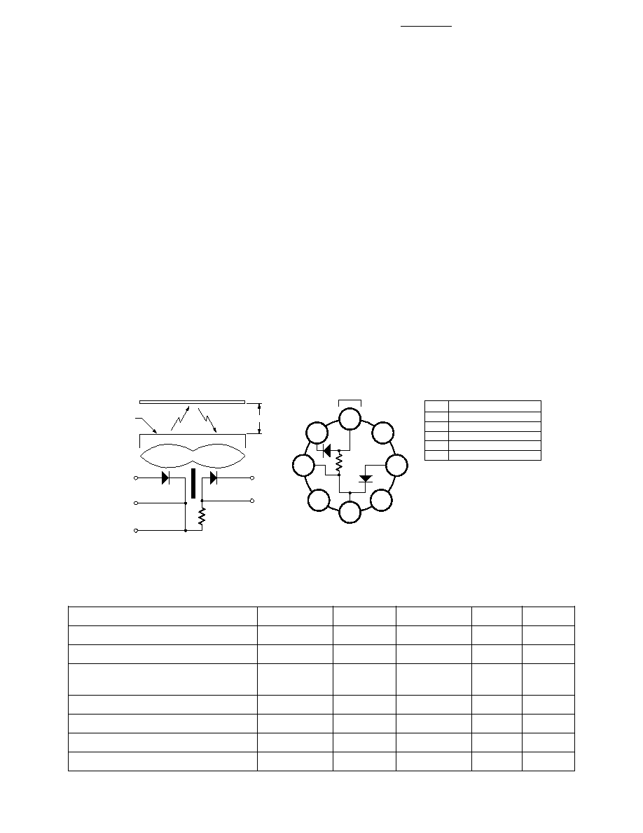
TOP VIEW
PIN #
FUNCTION
1
2
4
6
8
PHOTODIODE CATHODE
HEADER GROUND
**
LED ANODE
PHOTODIODE ANODE
**CUSTOMER SHOULD NOT CONNECT
GROUND TO PIN 4.
INTERNAL CONNECTION TO PIN 4
WILL BE DELETED IN THE FUTURE.
DPS
LED
SCHEMATIC DIAGRAM
CONNECTION DIAGRAM
1
8
REFERENCE
PLANE
REFLECTOR
6
CASE, SUBSTRATE
RS
DPS
1
8
LED
Z
2
4
RS ≠ CHARACTERISTIC NOT DEFINED
RS

3
Electrical/Optical Characteristics at T
A
= 25
∞
C
Parameter
Symbol
Min.
Typ.
Max.
Units
Conditions
Note
Figure
Reflected Photocurrent
I
pr
80
125
≠
nA
I
f
= 35 mA
4, 5, 11
1, 2, 4, 7
Quality Factor
<Q>
0.82
0.95
1.0
≠
I
f
= 35 mA
4, 6
Maximum Signal Point (MSP)
Z
4.01
4.27
4.52
mm
4, 7
4
(0.158) (0.168) (0.178)
(inch)
LED Forward Voltage
V
f
≠
1.72
1.86
V
I
f
= 35 mA
3
LED Reverse Breakdown Voltage
BVR
5.0
≠
≠
V
I
r
= 100
µ
A
Photodiode Dark Current
I
d
≠
50
1000
pA
V
d
= 5 V, I
f
= 0
8
LED Peak Wavelength
lambda
655
670
nm
I
f
= 35 mA
5
I
pr
Temperature Coefficient
K
e
-0.006
1/
∞
C
9
System Optical Step
d
0.154
mm
≠
10
8
Response Size (OSR)
(0.006)
(inch)
Notes:
1. CAUTION: The thermal constraints of the acrylic lens will not permit conventional wave soldering procedures. The typical preheat
and post-soldering cleaning procedures and dwell times can subject the lens to thermal stresses beyond the absolute maximum
ratings and can cause it to defocus.
2. (Reliability tests are proceeding--data not yet available.)
3. I
d
(max) = 100
µ
A. Recommended operation: V
d
(min) = 0 V V
d
(max) = 5 V Exceeding maximum conditions may cause permanent
damage to photodiode or to chip metallization.
4. Measured from a reflector coated with 99% diffuse reflective white paint (Kodak 6080) positioned 4.27 mm (0.168 in.) from the
reference plane. (See "Photocurrent Test Circuit" for test connection.) Measured physically is the total photocurrent, I
pt
, which
consists of a signal (reflected from target) component, I
pr
, and a component induced by reflection internal to the sensor (stray), I
ps
.
I
pt
= I
pr
+ I
ps
Specified is the reflected signal component, I
pr
.
5. See Bin Table.
6. <Q> = I
pr
/I
pt
.
7. Measured from the reference plane (R.P.) of the sensor.
8. Leakage current of photodiode measured in the dark.
9. Photocurrent variation with temperature varies with LED output which follows a natural exponential law:
I
p
(T) = I
p
(T
o
)*exp[K
e
(T-T
o
)].
10. OSR size is defined as the distance for a 10%-90% "step" response of I
pr
as the sensor moves over an abrupt step from opaque white
to black, or from opaque white to free space (no reflection).
11. Sensor contains no ambient light filtering--see Figure 6 for relative response of detector. In bright ambient light conditions, LED
signal may be a small portion of total signal. AC coupling and additional signal processing may be necessary. Reference Application
Note 1040.
4
IPT
nA-METER
REFERENCE
PLANE
REFLECTOR
6
CASE, SUBSTRATE
RS
DPS
1
8
LED
Z
2
4
If
+Vf
BIN #
MIN.
1
2
3
4
5
6
7
I
pr
LIMITS
MAX.
80
105
125
150
180
215
270
110 nA
135
155
190
220
275
320
BIN TABLE
DETECTOR
0.406 mm SQUARE
BAFFLE
SENSING
AREA
EMITTER
0.185 mm DIA. JUNCTION
ACRYLIC
SEAL
LENS
GLASS
Figure 1. Photocurrent Test Circuit.
OPTICAL SYSTEM
Product Marking
The photocurrent binning of the
sensor is incorporated as part of
the date code format, assigned at
time of test--"CTYYWWan",
where:
C = letter identifying country of
assembly--S = Singapore
If blank = USA
T = tester code designation letter
(single letter)
YY = last two digits of year
WW = week number in year
a = single lot code letter (A - Z),
sequential assignment during
week
n = bin number
See Figure 7 for suggestion in the
application of photocurrent bins.
Test algorithm bins units to the
lowest bin number if a unit is in
the overlap region. Such units can
cross bin boundaries as tempera-
ture changes. (Ambient tempera-
ture affects LED efficiency
slightly and may cause several
percent change in I
pr
). Bin
numbers are for "reference only"
and do not constitute an absolute
guarantee.
The output of all LEDs degrade
with time, depending on drive
conditions and temperature.
The entire available distribution
of parts, appropriately marked,
will be shipped. Single bin orders
cannot be supplied.

5
PHOTOCURRENT NORMALIZED
AT I
F
= 35 mA, 25 ∞C
3.0
IF ≠ FORWARD CURRENT ≠ mA
30
0
0
100
10
50
70 80
0.5
1.5
2.0
2.5
20
40
60
90
1.0
V
F
≠ FORWARD VOLTAGE ≠ V
2.0
IF ≠ FORWARD CURRENT
1.5
1.0
1 µA
100 mA
1.7
1.1
10 mA
1.2
1.9
10 µA 100 µA 1 mA
1.4
1.6
1.8
1.3
PHOTOCURRENT NORMALIZED
TO PEAK @ MSP
1.0
DISTANCE FROM REFERENCE PLANE
OF SENSOR ≠ mm
0
3.0
5.0
0.2
3.5
4.0
4.5
0.4
0.6
0.8
5.5
6.0
MSP = 4.01 mm
SENSOR
MSP RANGE
MSP = 4.52 mm
LED LIGHT OUTPUT
(NORMALIZED TO 25 ∞C VALUE)
1.75
WAVELENGTH ≠ nm
0
595
715
655
0.25
615
635
0.75
1.25
1.50
675
695
1.00
0.50
-20 ∞C
NORMALIZED
0 ∞C
NORMALIZED
25 ∞C
NORMALIZED
70 ∞C
NORMALIZED
RESPONSE NORMALIZED TO PEAK
1.0
WAVELENGTH ≠ nm
0
550
900
0.2
650
0.4
0.6
0.8
800
600
700
750
850
Figure 2. Relative Reflected Photocurrent.
Figure 3. LED Forward Voltage vs. Forward Current.
Figure 4. Photocurrent Variation with Distance.
Figure 5. 655 nm Emitter Typical Spectral Distribution.
Figure 6. Relative Spectral Response of Sensor.