 | ÐлекÑÑоннÑй компоненÑ: HFCT-5201 | СкаÑаÑÑ:  PDF PDF  ZIP ZIP |
Hfct5201.p65
Agilent HFCT-5201 155 Mb/s
Single Mode Fiber Transceiver for
ATM, SONET OC-3/SDH STM-1
Data Sheet
Description
General
The HFCT-5201 is a 1300 nm laser
based transceiver. It provides a
very cost-effective solution for
medium haul 155 Mb/s data link
requirements.
The new multisourced 2 x 9
footprint package style is a
variation of the standard 1 x 9
package with an integral Duplex
SC connector receptacle. The
extra row of 9 pins provides
connections for laser bias and
optical power monitoring as well
as providing transmitter disable
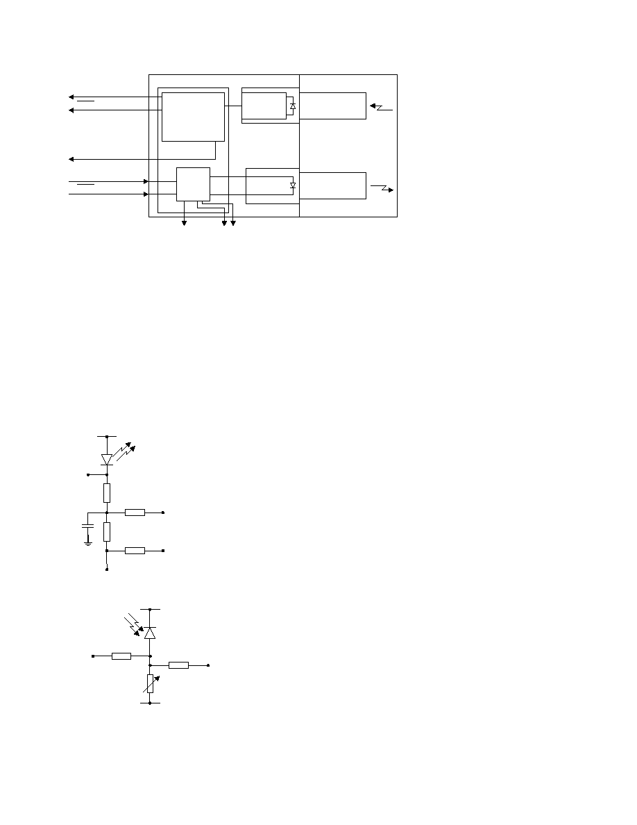
function. A block diagram is
shown in Figure 1.
Features
· 1300 nm Single mode transceiver
for links up to 15 Km
· Compliant with ATM forum
155 Mb/s physical layer
specification AF-PHY-0046.000
· Compliant with specifications
proposed to ANSI T1E1.2
committee for inclusion in
T1.646-1995 Broadband ISDN and
T1E1.2/96-002 SONET network to
customer installation interface
standards
· Compliant with specifications
proposed to ANSI T1X1.5
committee for inclusion in
T1.105.06 SONET physical layer
specifications standard
· Multisourced 2 x 9 pin-out
package style derived from 1 x 9
pin-out industry standard
package style
· Integral duplex SC connector
receptacle compliant with TIA/IA
and IEC standards
· Laser bias monitor, power monitor
and transmitter disable functions
compliant with SONET objectives
· Two Temperature Ranges:
0°C - +70°C
HFCT-5201B/D
-40°C - +85°C
HFCT-5201A/C
· Single +5 V power supply
operation and PECL logic
interfaces
· Wave solder and aqueous wash
process compatible
· Manufactured in an ISO 9001
certified facility
· Considerable EMI margin to FCC
Class B
Applications
· ATM 155 Mb/s links
· SONET OC-3/SDH STM-1
interconnections
2
Laser
AC
L
MON
(+)
Pin 6
V
CC
30 R
3 k
W
10 R
L
MON
( - )
Pin 5
Laser
DC Bias
3 k
W
V
CC
V
EE
30 k
W
V
REF
1.2 V
3 k
W
P
OWER
M
ONITOR
P
IN
9
(R
EF
TO
V
EE
)
ELECTRICAL SUBASSEMBLY
DATA
SIGNAL DETECT
DATA
POST
AMPLIFIER IC
LASER
DRIVER
IC
PRE-
AMPLIFIER
IC
LASER
PIN PHOTODIODE
DUPLEX SC
RECEPTACLE
TOP VIEW
OPTICAL
SUB-
ASSEMBLIES
DATA
DATA
POWER
MONITOR
LASER BIAS
MONITOR
Figure 1. Block Diagram
Figure 2a. Laser Bias Monitor
Figure 2b. Power Monitor Circuit
Transmitter Section
The transmitter section of the
HFCT-5201 consists of a 1300 nm
InGaAsP laser in an eyesafe optical
subassembly (OSA) which mates
to the fiber cable. The laser OSA is
driven by a custom, silicon bipolar
IC which converts differential
input PECL logic signals, ECL
referenced to a +5 V supply, into
an analog laser drive current.
The laser bias monitor circuit is
shown in Figure 2a, the power
monitor circuit in Figure 2b.
Receiver Section
The receiver utilizes an InGaAs
PIN photodiode mounted together
with a silicon bipolar
transimpedance preamplifier IC in
an OSA. This OSA is connected to
a silicon bipolar circuit providing
post- amplification quantization,
and optical signal detection.
The post amp circuit includes a
Signal Detect circuit which
provides a PECL logic-high output
upon detection of a usable input
optical signal level. Signal Detect
is a basic fiber failure indicator.
This single-ended PECL output is
designed to drive a standard PECL
input.
Receiver Signal Detect
As the input optical power is
decreased, Signal Detect will
switch from high to low (de-assert
point) somewhere between
sensitivity and the no light input
level. As the input optical power is
increased from very low levels,
Signal Detect will switch back
from low to high (assert point). The
assert level will be at least 0.5 dB
higher than the de-assert level.
Transceiver Specified for Wide
Temperature Range Operation
The HFCT-5201 is specified for
operation over normal commercial
temperature range of 0° to +70°C
(HFCT-5201B/D) or the extended
temperature range of -40° to +85°C
(HFCT-5201A/C) in an airflow of
2 m/s.
Other Members of Agilent SC Duplex
155 Mb/s Product Family
· HFCT-5205, 5103, 5215,
1300 nm single mode
transceivers for links up to
40 km. The part is based on the
1 x 9 industry standard package
and has an integral duplex SC
connector receptacle
· XMT5370155, 1300 nm laser-
based transmitter in pigtailed
package for 2 km and 15 km
links with SMF cables
· XMT5170155, 1300 nm laser-
based transmitter in pigtailed
package for 40 km links with
SMF cables
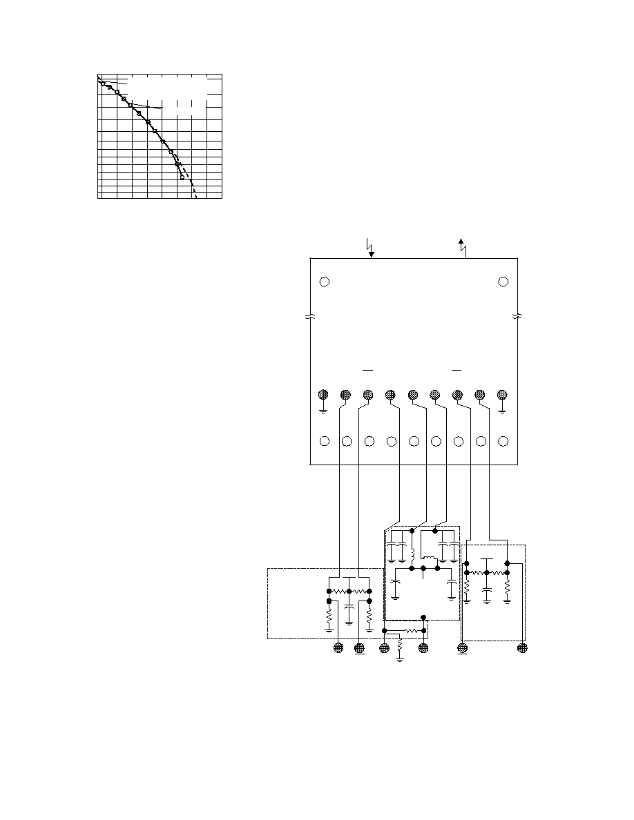
Applications Information
Typical BER Performance of
Receiver versus Input Optical Power
Level
The HFCT-5201 transceiver can be
operated at Bit-Error-Rate
conditions other than the required
BER = 1 x 10
-10
of the ATM Forum
155.52 Mb/s Physical Layer
Standard. The typical trade-off of
BER versus Relative Input Optical
Power is shown in Figure 3. The
Relative Input Optical Power in dB
is referenced to the Input Optical
Power parameter value in the
Receiver Optical Characteristics
table. For BER conditions better
than 1 x 10
-10
, more input signal is
needed (+dB).
3
10
-2
10
-3
10
-4
10
-5
10
-6
10
-7
10
-8
10
-9
10
-10
10
-11
10
-12
10
-13
10
-14
10
-15
-5
LINEAR EXTRAPOLATION OF
10
-4
THROUGH 10
-7
DATA
ACTUAL DATA
BIT ERROR RATIO
-4 -3 -2
-1
0
1
2
3
Figure 3. Relative Input Optical Power
- dBm. Avg.
C8
Rx
Tx
NO INTERNAL
CONNECTION
NO INTERNAL
CONNECTION
TOP VIEW
V
EER
18
RD
17
RD
16
SD
15
V
CCR
14
V
CCT
13
TD
12
TD
11
V
EET
10
NC
1
NC
2
NC
3
NC
4
NC
8
R8
RD
RD
TERMINATE
AT THE
DEVICE
INPUTS
SD
C3
C4
LOCATE
FILTER
AT VCC
PINS
V
CC
L1 L2
V
CC
R5
R7
R6
C6
R4
V
CC
R2
R3
R1
C5
TD
TERMINATE AT
FIBER-OPTIC
TRANSCEIVER
INPUTS
TD
NOTES:
THE SPLIT-LOAD TERMINATIONS FOR PECL SIGNALS NEED TO BE LOCATED AT THE INPUT OF
DEVICES RECEIVING THOSE PECL SIGNALS.
R1 = R4 = R6 = R8 = R10 = 130
W
R2 = R3 = R5 = R7 = R9 = 82
W
C1 = C2 = 10 µF
C3 = C4 = C7 = C8 = 100 nF
C5 = C6 = 0.1 µF.
L1 = L2 = 3.3 µH COIL.
L
MON
(-)
5
L
MON
(+)
6
Tx
DIS
7
P
MON
9
R10
C1 C7
C2
R9
Figure 4. Recommended Circuit Schematic
Recommended Circuit Schematic
In order to ensure proper
functionality of the HFCT-5201 a
recommended circuit is provided
in Figure 4. When designing the
circuit interface, there are a few
fundamental guidelines to follow.
For example, in the Recommended
Circuit Schematic figure the
differential data lines should be
treated as 50 ohm Microstrip or
stripline transmission lines. This
will help to minimize the parasitic
inductance and capacitance
effects. Proper termination of the
differential data signals will
prevent reflections and ringing
which would compromise the
signal fidelity and generate
unwanted electrical noise. Locate
termination at the received signal
end of the transmission line. The
length of these lines should be
kept short and of equal length. For
the high speed signal lines,
differential signals should be
used, not single-ended signals, and
these differential signals need to
be loaded symmetrically to
prevent unbalanced currents from
flowing which will cause
distortion in the signal.
Maintain a solid, low inductance
ground plane for returning signal
currents to the power supply.
Multilayer plane printed circuit
board is best for distribution of
V
CC
, returning ground currents,
forming transmission lines and
shielding, Also, it is important to
suppress noise from influencing
the fiber-optic transceiver
performance, especially the
receiver circuit. Proper power
supply filtering of V
CC
for this
transceiver is accomplished by
using the recommended separate
filter circuits shown in Figure 4,
the Recommended Circuit
Schematic diagram for the
transmitter and receiver sections.
These filter circuits suppress V
CC
noise of 100 mV peak-to-peak or
less over a broad frequency range.
This prevents receiver sensitivity
degradation due to V
CC
noise. It is
recommended that surface-mount
components be used. Use tantalum
capacitors for the 10 µF capacitors
and monolithic, ceramic bypass
capacitors for the 0.1 µF
capacitors. Also, it is
4
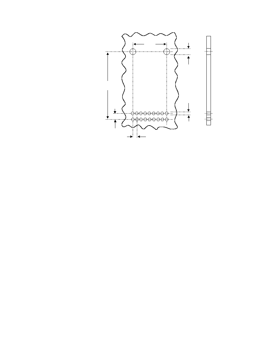
TOP VIEW
20.32
(0.8)
2 x Ø 1.9 ± 0.1
(0.075 ±0.004)
33.02
(1.3)
2.54
(0.1)
2.54
(0.1)
18 x Ø 0.8 ± 0.1
(0.031 ±0.004)
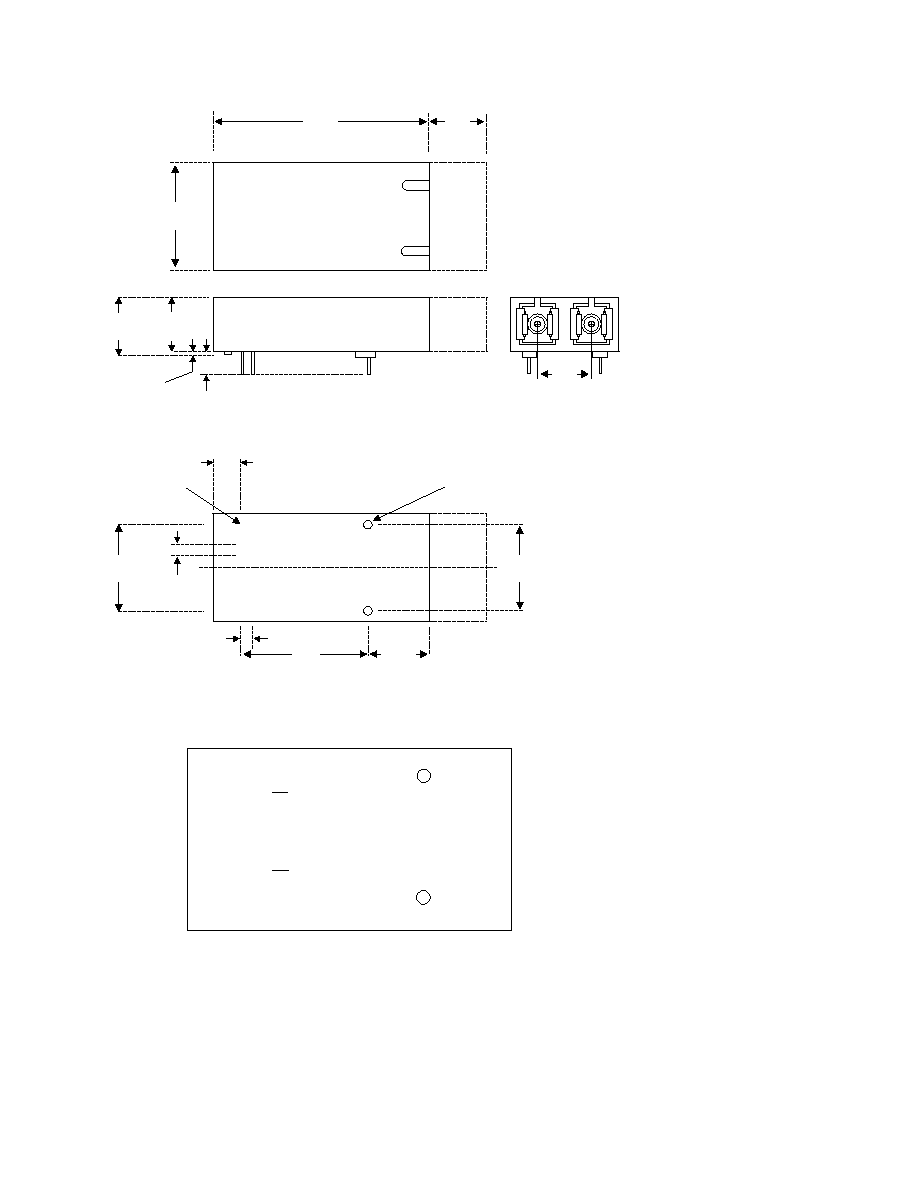
Figure 5. Recommended Board Layout Hole Pattern
recommended that a surface-
mount coil inductor of
3.3 µH be used. Ferrite beads can
be used to replace the coil
inductors when using quieter V
CC
supplies, but a coil inductor is
recommended over a ferrite bead.
Coils with a low, series dc
resistance (<0.7 ohms) and high,
self-resonating frequency are
recommended. All power supply
components need to be placed
physically next to the V
CC
pins of
the receiver and transmitter. Use a
good, uniform ground plane with a
minimum number of holes to
provide a low-inductance ground
current return for the power
supply currents.
Evaluation Circuit Boards
Evaluation circuit boards imple-
menting this recommended circuit
design are available from Agilent's
Application Engineering staff.
Contact your local Agilent sales
representative to arrange for
access to one if needed.
Operation in -5.2 V Designs
For applications that require -5.2 V
dc power supply level for true ECL
logic circuits, the HFCT-5201
transceiver can be operated with a
V
CC
= 0 V dc and a V
EE
= -5.2 V dc.
This transceiver is not specified
with an operating, negative power
supply voltage. The potential
compromises that can occur with
use of -5.2 V dc power are that the
absolute voltage states for V
OH
and V
OL
will be changed slightly
due to the 0.2 V difference in
supply levels. Also, noise
immunity may be compromised
for the HFCT-5201 transceiver
because the ground plane is now
the V
CC
supply point. The
suggested power supply filter
circuit shown in Figure 4,
Recommended Circuit Schematic,
should be located in the V
EE
paths
at the transceiver supply pins.
Direct coupling of the differential
data signals can be done between
the HFCT-5201 transceiver and
the standard ECL circuits.
Recommended Solder and Wash
Process
The HFCT-5201 is compatible with
industry standard wave or hand
solder processes.
HFCT-5201 Process Plug
The HFCT-5201 transceiver is
supplied with a process plug for
protection of the optical ports
with the Duplex SC connector
receptacle. This process plug
prevents contamination during
wave solder and aqueous rinse as
well as during handling, shipping
or storage. It is made of
high-temperature, molded, sealing
material.
Recommended Solder Fluxes
and Cleaning/Degreasing
Chemicals
Solder fluxes used with the
HFCT-5201 fiber-optic transceiver
should be water-soluble, organic
solder fluxes. Some recommended
solder fluxes are Lonco 3355-11
from London Chemical West, Inc.
of Burbank, CA, and 100 Flux from
Alpha- metals of Jersey City, NJ.
Recommended cleaning and
degreasing chemicals for the
HFCT-5201 are alcohol's (methyl,
isopropyl, isobutyl), aliphatics
(hexane, heptane) and other
chemicals, such as soap solution
or naphtha. Do not use partially
halogenated hydrocarbons for
cleaning/degreasing. Examples of
chemicals to avoid are 1.1.1.
trichloroethane, ketones (such as
MEK), acetone, chloroform, ethyl
acetate, methylene dichloride,
phenol, methylene chloride or
N-methylpyrolldone.
5
Figure 6. Package Outline Drawing and Pinout
AREA
RESERVED
FOR
PROCESS
PLUG
52.02
(2.048)
MAX
12.7
(0.5)
25.4
(1.0)
MAX
11.1
(0.437)
10.35
(0.407)
MAX
MAX
0.75
(0.03)
3.3
(0.13)
12.7
(0.5)
+
+
18 x Ø 0.46
(0.018)
0.53
(0.021)
Note 1
Note 1: SOLDER POSTS AND ELECTRICAL PINS ARE TIN/LEAD PLATED.
DIMENSIONS IN MILLIMETERS (INCHES).
20.32
(0.8)
8 x 2.54
(0.1)
MIN
MAX
3.12
(0.123)
2.54
(0.1)
33.02
(1.3)
15.88
(0.625)
2 x Ø 1.27
(0.05)
1.32
(0.052)
Note 1
MAX
MIN
20.32
(0.8)
ff 18 = V
EER
ff 17 = RD
ff 16 = RD
ff 15 = SD
ff 14 = V
CCR
ff 13 = V
CCT
ff 12 = TD
ff 11 = TD
ff 10 = V
EET
1 = N/C
2 = N/C
3 = N/C
4 = N/C
5 = L
MON
(-)
6 = L
MON
(+)
7 = T
X
DIS
8 = N/C
9 = P
MON
RX
TX
N/C
N/C
TOP VIEW
Document Outline
- Features
- Applications
- Description
- Transmitter Section
- Receiver Section
- Receiver Signal Detect
- Transceiver Specified for Wide Temperature Range Operation
- Other Members of Agilent SC Duplex 155 Mb/s Product Family
- Applications Information
- Typical BER Performance of Receiver versus Input Optical Power Level
- Recommended Circuit Schematic
- Figure 4
- Figure 5
- Figure 6
- Evaluation Circuit Boards
- Operation in -5.2 V Designs
- Recommended Solder and Wash Process
- HFCT-5201 Process Plug
- Recommended Solder Fluxes and Cleaning/Degreasing Chemicals
- Regulatory Compliance
- Table 1
- Electrostatic Discharge (ESD)
- Electromagnetic Interference (EMI)
- Immunity
- Performance Specifications
- Absolute Maximum Ratings
- Operating Environment
- Transmitter Section
- Receiver Section
- Table 2. Pin Out Table
- Ordering Information
- Supporting Documentation