 | –≠–Ľ–Ķ–ļ—ā—Ä–ĺ–Ĺ–Ĺ—č–Ļ –ļ–ĺ–ľ–Ņ–ĺ–Ĺ–Ķ–Ĺ—ā: INA-01100 | –°–ļ–į—á–į—ā—Ć:  PDF PDF  ZIP ZIP |
Document Outline
- List of Figures
- 1. Typical Gain and Noise Figure vs. Frequency
- 2. Device Current vs. Voltage
- 3. Power Gain vs. Current
- 4. Output Power and 1 dB Gain Compression, NF and Power Gain vs. Case Temperature
- 5. Output Power at 1 dB Gain Compression vs. Frequency
- 6. Noise Figure vs. Frequency
- Features
- Description
- Typical Biasing Configuration
- Chip Outline
- INA-01100 Absolute Maximum Ratings
- INA-01100 Electrical Specifications [1,3] , TA = 25įC
- INA-01100 Typical Scattering Parameters [1] (Z = 50 W, T = 25įC, V = 35 mA)
- INA-01100 Typical Performance, T A = 25įC
- INA-01100 Chip Dimensions
6-84
Low Noise, Cascadable
Silicon Bipolar MMIC Amplifier
Technical Data
Features
∑ Cascadable 50
Gain Block
∑ Low Noise Figure:
1.7 dB Typical at 100 MHz
∑ High Gain:
32.5 dB Typical at 100 MHz
∑ 3 dB Bandwidth:
DC to 500 MHz
∑ Unconditionally Stable
(k>1)
INA-01100
Chip Outline
[1]
Description
The INA-01100 is a low-noise silicon
bipolar Monolithic Microwave
Integrated Circuit (MMIC) feedback
amplifier chip. It is designed for
narrow or wide bandwidth indus-
trial and military applications that
require high gain and low noise IF
or RF amplification.
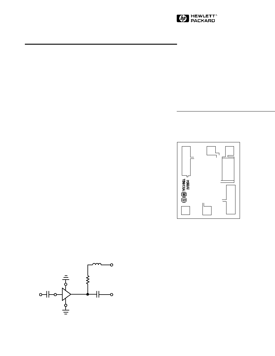
Typical Biasing Configuration
C
block
C
block
R
bias
V
CC
V
d
= 5.5 V
(Nominal)
RFC (Optional)
RF IN
RF OUT
4
1
2
3
Note:
1. See Application Note, "A005: Transistor
Chip Use" for additional information.
RF
IN
RF
OUT
GND
2
GND
1
The INA series of MMICs is
fabricated using HP's 10 GHz f
T
,
25 GHz f
MAX
, ISOSATTM-I silicon
bipolar process which uses nitride
self-alignment, submicrometer
lithography, trench isolation, ion
implantation, gold metallization
and polyimide intermetal dielec-
tric and scratch protection to
achieve excellent performance,
uniformity and reliability.
The recommended assembly
procedure is gold-eutectic die
attach at 400
į
C and either wedge
or ball bonding using 0.7 mil gold
wire.
[1]
5965-9561E
6-85
INA-01100 Absolute Maximum Ratings
Parameter
Absolute Maximum
[1]
Device Current
50 mA
Power Dissipation
[2,3]
400 mW
RF Input Power
+13 dBm
Junction Temperature
200
į
C
Storage Temperature
≠65 to 200
į
C
Thermal Resistance:
jc
= 60
į
C/W
Notes:
1. Permanent damage may occur if
any of these limits are exceeded.
2. T
Mounting Surface
(T
MS
)
= 25
į
C.
3. Derate at 16.7 mW/
į
C for T
MS
>
176
į
C.
INA-01100 Typical Scattering Parameters
[1]
(Z
O
= 50
, T
A
= 25
į
C, V
CC
= 35 mA)
Freq.
GHz
Mag
Ang
dB
Mag
Ang
dB
Mag
Ang
Mag
Ang
k
0.01
0.09
≠16
32.7
43.4
≠1
≠38.5
.012
≠1
.18
1
1.17
0.05
0.10
≠27
32.7
43.1
≠10
≠38.6
.012
15
.19
5
1.18
0.10
0.11
≠5
32.4
41.9
≠20
≠38.4
.012
≠8
.20
10
1.17
0.20
0.14
≠80
31.6
38.0
≠37
≠38.6
.012
4
.24
14
1.22
0.30
0.18
≠98
30.5
33.7
≠52
≠38.8
.011
≠10
.27
15
1.31
0.40
0.20
≠110
29.4
29.6
≠65
≠39.6
.011
2
.30
10
1.51
0.50
0.22
≠115
28.4
26.2
≠75
≠38.6
.012
≠12
.32
6
1.48
0.60
0.24
≠120
27.4
23.4
≠84
≠39.1
.011
≠7
.34
1
1.67
0.80
0.27
≠124
25.7
19.3
≠100
≠38.3
.012
≠6
.36
≠11
1.76
1.00
0.30
≠127
24.3
16.3
≠115
≠36.1
.016
≠5
.36
≠22
1.58
1.5
0.44
165
21.8
12.37 ≠179
≠33.6
.020
42
.19
≠69
1.75
2.0
0.44
154
17.9
7.88
146
≠33.0
.022
42
.13
≠106
2.42
2.5
0.46
148
14.6
5.36
121
≠30.6
.029
36
.12
≠151
2.63
3.0
0.48
139
11.4
3.71
96
≠30.0
.032
45
.10
159
3.31
Note:
1. S-parameters are de-embedded from 70 mil package measured data using the package model found in the DEVICE
MODELS section of the Communications Components Designer's Catalog.
S
11
S
21
S
12
S
22
G
P
Power Gain (|S
21
|
2
)
f = 100 MHz
dB
32.5
G
P
Gain Flatness
f = 10 to 250 MHz
dB
Ī
0.5
f
3 dB
3 dB Bandwidth
MHz
500
ISO
Reverse Isolation (|S
12
|
2
)
f = 10 to 250 MHz
dB
39
Input VSWR
f = 10 to 250 MHz
1.6:1
Output VSWR
f = 10 to 250 MHz
1.5:1
NF
50
Noise Figure
f = 100 MHz
dB
1.7
P
1 dB
Output Power at 1 dB Gain Compression
f = 100 MHz
dBm
11
IP
3
Third Order Intercept Point
f = 100 MHz
dBm
23
t
D
Group Delay
f = 100 MHz
psec
200
V
d
Device Voltage
V
4.0
5.5
7.0
dV/dT
Device Voltage Temperature Coefficient
mV/
į
C
+10
Notes:
1. The recommended operating current range for this device is 30 to 40 mA. Typical performance as a function of current
is on the following page.
2. RF performance of the chip is determined by packaging and testing 10 devices per wafer.
3. The values are the achievable performance for the INA-01100 mounted in a 70 mil stripline package.
INA-01100 Electrical Specifications
[1,3]
, T
A
= 25
į
C
Symbol
Parameters and Test Conditions
[2]
: I
d
= 35 mA, Z
O
= 50
Units
Min.
Typ.
Max.
VSWR
6-86
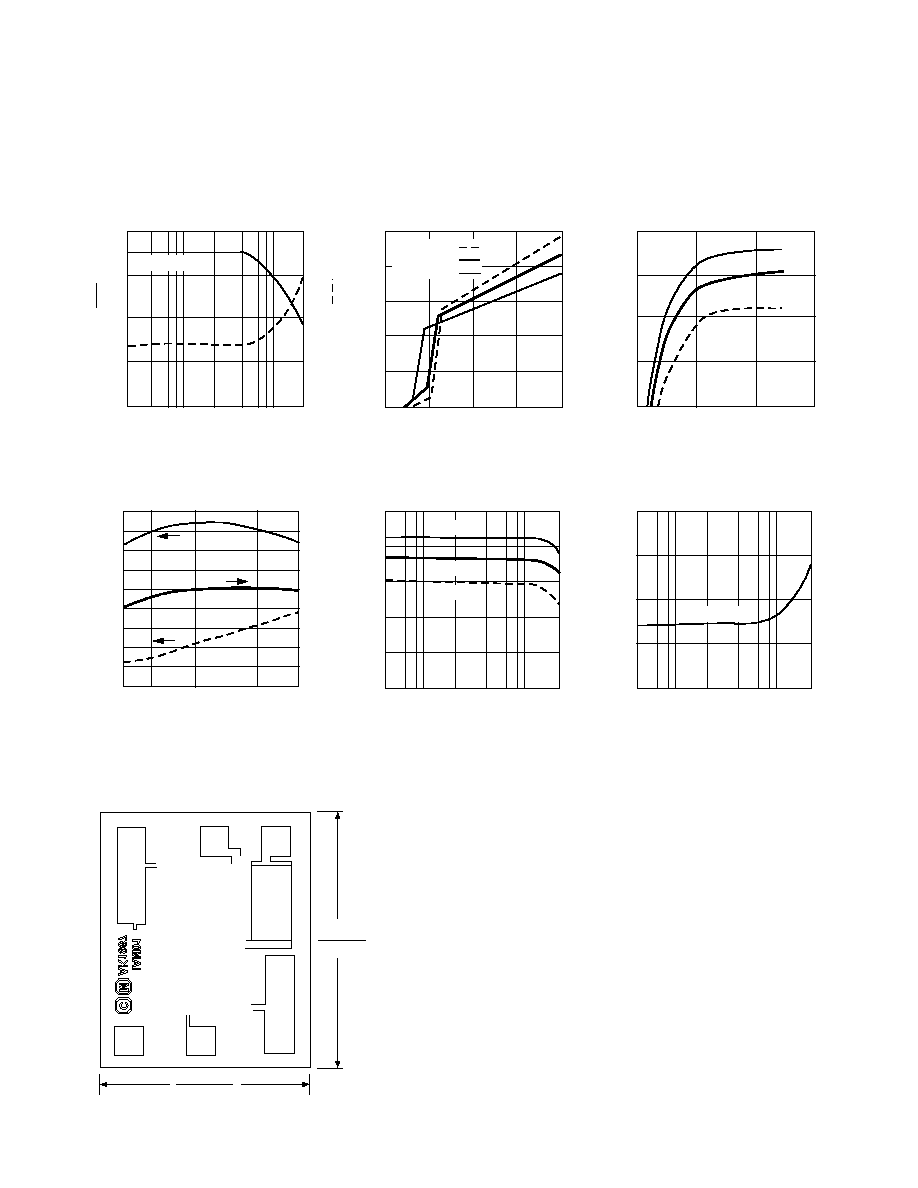
INA-01100 Typical Performance, T
A
= 25
į
C
(unless otherwise noted: The values are the achievable performance for the INA-01100 mounted in a 70 mil
stripline package.)
0
10
20
30
40
50
I
d
(mA)
I
d
(mA)
I
d
(mA)
0
4
6
2
8
V
d
(V)
Figure 2. Device Current vs. Voltage.
FREQUENCY (GHz)
FREQUENCY (GHz)
Figure 5. Output Power at 1 dB Gain
Compression vs. Frequency.
Figure 6. Noise Figure vs. Frequency.
NF (dB)
15
20
25
30
35
1.0
.01
.02
.05
0.1
0.2
0.5
1.0
1.5
2.0
2.5
3.0
G
p
(dB)
NF (dB)
FREQUENCY (GHz)
Figure 1. Typical Gain and Noise Figure
vs. Frequency, T
A
= 25
į
C, I
d
= 35 mA
Gain Flat to DC
T
MS
= +125
į
C
T
MS
= +25
į
C
T
MS
= ≠55
į
C
15
20
25
30
35
.01
.05
0.2
1.0
Figure 3. Power Gain vs. Current.
0.1 GHz
1.0 GHz
0.5 GHz
0.5
2.0
1.5
2.5
1.0
30
31
32
33
7
9
11
13
≠55
≠25
+25
+85
+125
.02
.05
0.1
0.5
0.2
1.0
.02
.05
0.1
0.5
0.2
1.0
NF (dB)
0
9
6
15
12
3
1.0
2.5
2.0
3.0
1.5
P
1 dB
(dBm)
P
1 dB
(dBm)
G
p
(mA)
TEMPERATURE (
į
C)
Figure 4. Output Power and 1 dB Gain
Compression, NF and Power Gain vs.
CaseTemperature. f = 0.1 GHz, I
d
= 35 mA.
G
p
P
1 dB
NF
I
d
= 40 mA
I
d
= 35 mA
I
d
= 30 mA
I
d
= 30 to 40 mA
375
Ī
13
Ķ
m
14.8
Ī
0.5 mil
(4)
(3)
(1)
(2)
RF
IN
RF
OUT
GND
2
GND
1
500
Ī
13
Ķ
m
19.7
Ī
0.5 mil
Chip thickness is 140
Ķ
m/5.5 mil. Bond Pads are
41
Ķ
m/1.6 mil typical on each side. Note: Ground
Bonding is Critical. Refer to Application Bulletin,
"AB-0007: INA Bonding Configuration".
INA-01100 Chip Dimensions