
6-192
2 ≠ 6 GHz Cascadable GaAs
MMIC Amplifier
Technical Data
Features
∑ Cascadable 50
Gain Block
∑ Broadband Performance:
2≠6 GHz
12.0 dB Typical Gain
±
0.8 dB Gain Flatness
12.0 dBm P
1 dB
∑ Single Supply Bias
∑ Cost Effective Ceramic
Microstrip Package
MGA-64135
Description
The MGA-64135 is a high perfor-
mance gallium arsenide Monolithic
Microwave Integrated Circuit
(MMIC) housed in a cost effective,
microstrip package. This device is
designed for use as a general
purpose 50 ohm gain block in the 2
to 6 GHz frequency range. Typical
35 Micro-X Package
Typical Biasing Configuration
C
block
V
d
RFC
IN
1
4
3
2
OUT
MGA
applications include narrow and
broadband IF and RF amplifiers
for commercial, industrial, and
military requirements.
This MMIC is a cascade of two
stages, each utilizing shunt
feedback to establish a broadband
impedance match. The source of
each stage is AC grounded to
allow biasing from a single
positive power supply. The
interstage blocking capacitor as
well as a resistive "self-bias"
network are included on chip.
The die is fabricated using HP's
nominal .5 micron recessed
Schottky-barrier-gate, gold
metallization and silicon nitride
passivation to achieve excellent
performance, uniformity, and
reliability.
5965-9005E
6-193
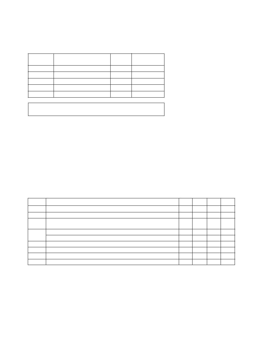
MGA-64135 Absolute Maximum Ratings
Absolute
Symbol
Parameter
Units
Maximum
[1]
V
d
Device Voltage
V
12
P
diss
Total Power Dissipation
[2]
mW
650
P
in
CW RF Input Power
dBm
+13
T
ch
Channel Temperature
∞
C
175
T
STG
Storage Temperature
[3]
∞
C
-65 to 175
Notes:
1. Operation of this device above any one of these parameters may cause
permanent damage.
2. Derate linearly at 8.3 mW/
∞
C for
T
CASE
> 103
∞
C.
3. Storage above +150
∞
C may tarnish the leads of this package making it
difficult to solder into a circuit. After a device has been soldered into a
circuit, it may be safely stored up to 175
∞
C.
4. The thermal resistance value is based on measurements taken with the
device soldered to a 25 mil Teflon PCB.
5. The small spot size of this technique results in a higher, though more
accurate determination of
jc
than do alternate methods. See MEASURE-
MENTS section for more information.
Thermal Resistance :
jc
= 150
∞
C/W
[4]
; T
CH
= 150
∞
C
Liquid Crystal Measurement:
1
µ
m Spot Size
[5]
G
P
Power Gain (|S
21
|
2
)
f = 2 to 6 GHz
dB
10.0
12.0
G
P
Gain Flatness
f = 2 to 6 GHz
dB
±
1.20
--
Gain Variation vs. Temperature
f = 2 to 6 GHz
dB
±
0.5
T
CASE
= ≠25
∞
C to +85
∞
C
Input VSWR
f = 2 to 6 GHz
1.5:1
2.0:1
Output VSWR
f = 2 to 6 GHz
1.4:1
2.0:1
P
1 dB
Output Power at 1 dB Gain Compression
f = 2 to 6 GHz
dBm
10.0
12.0
NF
50
Noise Figure
f = 2 to 6 GHz
dB
7.5
--
Reverse Isolation (|S
21
|
2
)
f = 2 to 6 GHz
dB
35
I
d
Device Current
mA
35
50
65
MGA-64135 Electrical Specifications, T
A
= 25
∞
C
Symbol
Parameters and Test Conditions: V
d
= 10 V, Z
O
= 50
Units
Min.
Typ.
Max.
VSWR

6-194
MGA-64135 Typical Performance, T
A
= 25
∞
C
MGA-64135 Typical Scattering Parameters (Z
O
= 50
, T
A
= 25
∞
C, V
d
= 10 V)
Freq.
GHz
Mag
Ang
dB
Mag
Ang
dB
Mag
Ang
Mag
Ang
0.5
.27
≠38
10.6
3.38
174
≠31.0
.028
≠13
.38
≠41
1.0
.18
≠44
12.9
4.42
≠9
≠33.1
.022
≠20
.26
≠48
2.0
.14
≠67
14.3
5.21
≠54
≠34.9
.018
≠19
.16
≠59
3.0
.17
≠91
14.5
5.33
≠93
≠37.1
.014
≠21
.11
≠75
4.0
.20
≠105
14.2
5.11
≠131
≠37.8
.013
≠15
.11
≠71
5.0
.18
≠114
13.6
4.79
≠167
≠37.3
.014
≠10
.14
≠57
6.0
.07
≠162
12.8
4.35
157
≠38.5
.012
≠1
.17
≠41
7.0
.15
96
11.8
3.89
123
≠36.0
.016
3
.16
≠42
8.0
.23
76
10.8
3.46
92
≠34.3
.019
4
.10
≠54
9.0
.32
63
9.5
2.98
63
≠29.3
.034
12
.04
159
10.0
.43
52
8.6
2.68
38
≠27.6
.041
≠11
.09
116
S
11
S
21
S
12
S
22
0
6.0
8.0
2.0
4.0
10.0
0
4.0
6.0
2.0
8.0
FREQUENCY (GHz)
FREQUENCY (GHz)
Figure 2. Output Power @ 1 dB Gain
Compression vs. Frequency, V
d
= 10 V.
6
8
10
16
14
12
G
P
(dB)
11
12
13
14
15
P
1 dB
(dBm)
2.0
6.0
4.0
8.0
FREQUENCY (GHz)
7.0
7.5
8.0
8.5
9.0
NOISE FIGURE
(dB)
Figure 1. Power Gain vs. Frequency,
V
d
= 10 V.
Figure 3. Noise Figure vs. Frequency,
V
d
= 10 V.
0
6.0
8.0
2.0
4.0
10.0
FREQUENCY (GHz)
INPUT
1.0:1
1.2:1
1.4:1
2.0:1
1.8:1
1.6:1
VSWR
Figure 4. VSWR vs. Frequency, V
d
= 10 V.
OUTPUT

6-195
1
3
4
2
GROUND
DIA.
GROUND
RF OUTPUT
RF INPUT
.085
2.15
641
.083
2.11
.020
.508
.100
2.54
.455
±
.030
11.54
±
.75
.006
±
.002
.15
±
.05
Notes:
(unless otherwise specified)
1. Dimensions are in
2. Tolerances
in .xxx =
±
0.005
mm .xx =
±
0.13
mm
.022
.56
.057
±
.010
1.45
±
.25
35 Micro-X Package Dimensions