 | ÐлекÑÑоннÑй компоненÑ: MGS-71008 | СкаÑаÑÑ:  PDF PDF  ZIP ZIP |
Äîêóìåíòàöèÿ è îïèñàíèÿ www.docs.chipfind.ru
7-161
Absorptive SPDT GaAs MMIC
Switch
Technical Data
Features
· Single-Pole, Double-Throw
Output
· Broad Bandwidth:
DC to 3 GHz
· High Isolation:
37 dB Typical at 1 GHz
· Fast Switching Time:
3 ns Typical
· Ultra Low DC Power
Consumption
· Small Surface-Mount Plastic
Package
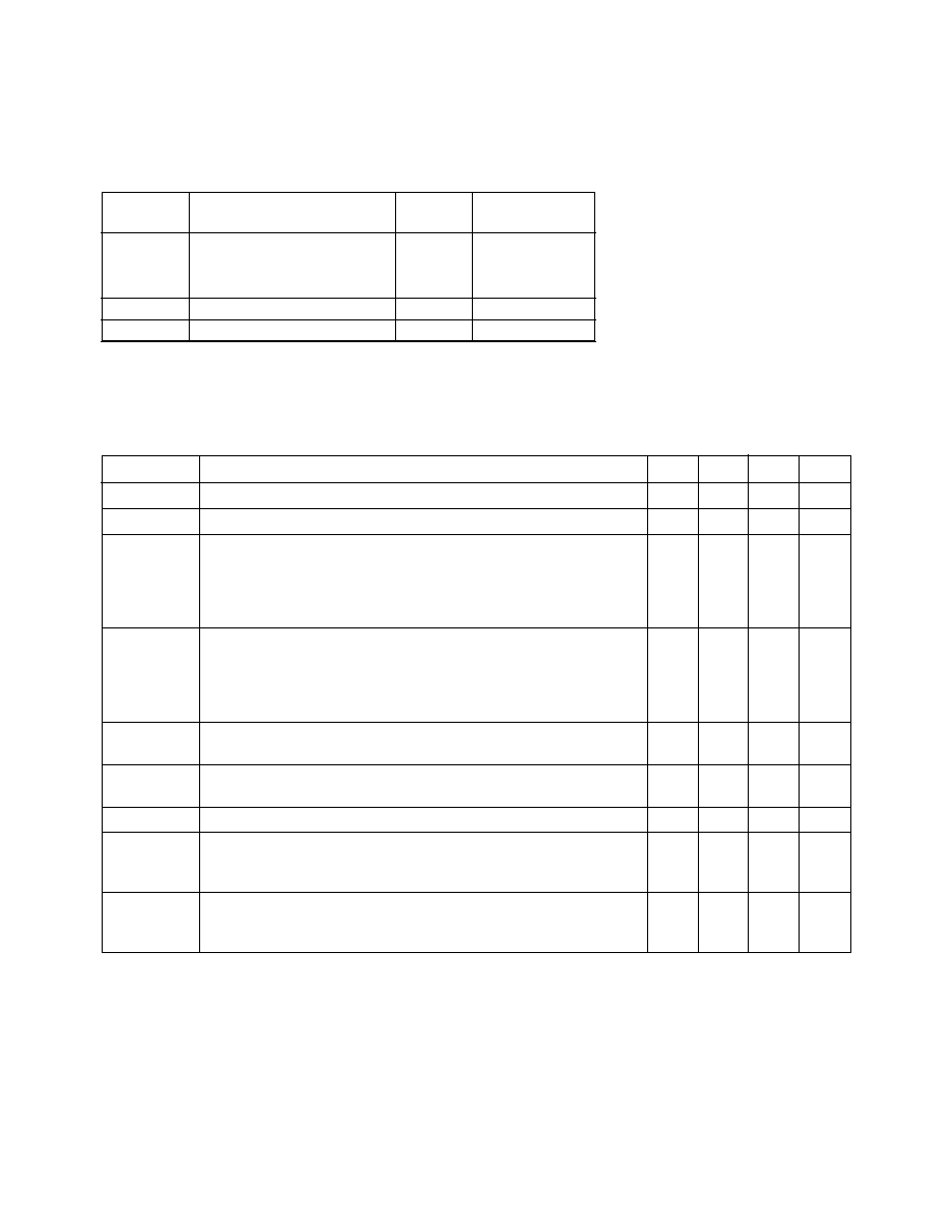
MGS-71008
SO-8 Package
Description
The MGS-71008 is a single-pole,
double-throw monolithic GaAs
MMIC switch. The J2 and J3 of the
MGS-71008 are terminated to
ground by internal 50
load
resistors when "off" (a reflective
version, the MGS-70008, which
terminates the "off" port to
ground, is also available). The
switch is sealed in a small, plastic,
AC Equivalent
Circuit/Pinout
J1
Ground
J2
Control 1
Control 2
J3
Ground
Ground
surface-mount SO-8 package.
Switching is actuated by a -5 V
control voltage per the truth table
shown on the next page. -3.3 V
operation is also possible with
some reduction in P
1 dB
and IP
3
.
The MGS-71008 is designed for
high volume commercial applica-
tions where low insertion loss,
high isolation, and fast switching
speed are required. Its low cost
and high performance make it
suitable for a wide variety of uses
such as digital cellular, spread
spectrum, GPS, and other RF
switching applications. Refer to
applications note AN-G007 for
more application details.
The die is fabricated using HP's
nominal 0.3 micron recessed
Schottky-barrier-gate, gold
metallization, and silicon nitride
passivation to achieve excellent
performance, uniformity, and
reliability.
5965-9118E
7-162
MGS-71008 Absolute Maximum Ratings
Absolute
Symbol
Parameter
Units
Maximum
[1]
Maximum Input Power
below 500 MHz
dBm
+27
above 500 MHz
dBm
+30
Control Voltage
V
-8.0
T
STG
Storage Temperature
°
C
-65 to 150
Note:
1. Operation of this device above any one of these limits may cause permanent
damage.
Electrical Specifications, T
A
= 25
°
C
Symbol
Parameters and Test Conditions
[1]
Units Min.
Typ. Max.
I
C
Control Input Current
DC
µ
A
12
110
BW
Bandwidth
GHz
DC-3
IL
Insertion Loss
200 MHz
dB
0.9
1000 MHz
dB
1.2
1.5
2000 MHz
dB
1.3
2500 MHz
dB
1.4
3000 MHz
dB
1.5
ISO
Isolation
200 MHz
dB
52
1000 MHz
dB
30
37
2000 MHz
dB
26
2500 MHz
dB
22
3000 MHz
dB
16
VSWR
Voltage Standing Wave Ration (on port)
DC - 1000 MHz
--
1.2:1
1.4:1
J1, J2 or J3
1000-3000 MHz
--
1.3:1
VSWR
Voltage Standing Wave Ration (off port)
DC - 2000 MHz
--
1.2:1
J2 or J3
2000-3000 MHz
--
1.3:1
I
SW
Switching Speed
10% to 90%
ns
3
P
1 dB
[2]
Output @ 1 dB Gain Compression
200 MHz
dBm
16.5
1000 MHz
dBm
25.2
2000 MHz
dBm
25.2
IP
3
[2]
3rd Order Intercept
200 MHz
dBm
41
1000 MHz
dBm
45
2000 MHz
dBm
45
Notes:
1. Measured in a 50
system at 1 GHz, unless otherwise specified, V
C
= -5 V.
2. Measured in a 50
system with V
C
= -7 V.
7-163
MGS-70008 Typical Performance, T
A
= 25
°
C
MGS-71008 Truth Table (Typical Performance at 1 GHz)
Control Input
Insertion Loss
Return Loss
C1
C2
J1-J2
J1-J3
J1
J2
J3
0 V
0 V
16 dB
16 dB
1 dB
1 dB
1 dB
For normal SPDT use
0 V
-5 V
37 dB
1.2 dB
22 dB
22 dB
22 dB
For normal SPDT use
-5 V
0 V
1.2 dB
37 dB
22 dB
22 dB
1 dB
-5 V
-5 V
26 dB
26 dB
1 dB
1 dB
1 dB
MGS-71008 Typical Power Performance vs. Frequency and Control Voltage (V
C
)
(All other typical specifications remain constant.)
V
C
= -7 V
V
C
= -5 V
V
C
= -3.3 V
Frequency
P
1 dB
IP
3
P
1 dB
IP
3
P
1 dB
IP
3
200 MHz
16.5 dBm
41 dBm
16.5 dBm
41 dBm
15.5 dBm
35 dBm
1000 MHz
25.2 dBm
45 dBm
23.7 dBm
44 dBm
19.0 dBm
38 dBm
2000 MHz
25.2 dBm
45 dBm
22.5 dBm
44 dBm
18.5 dBm
38 dBm
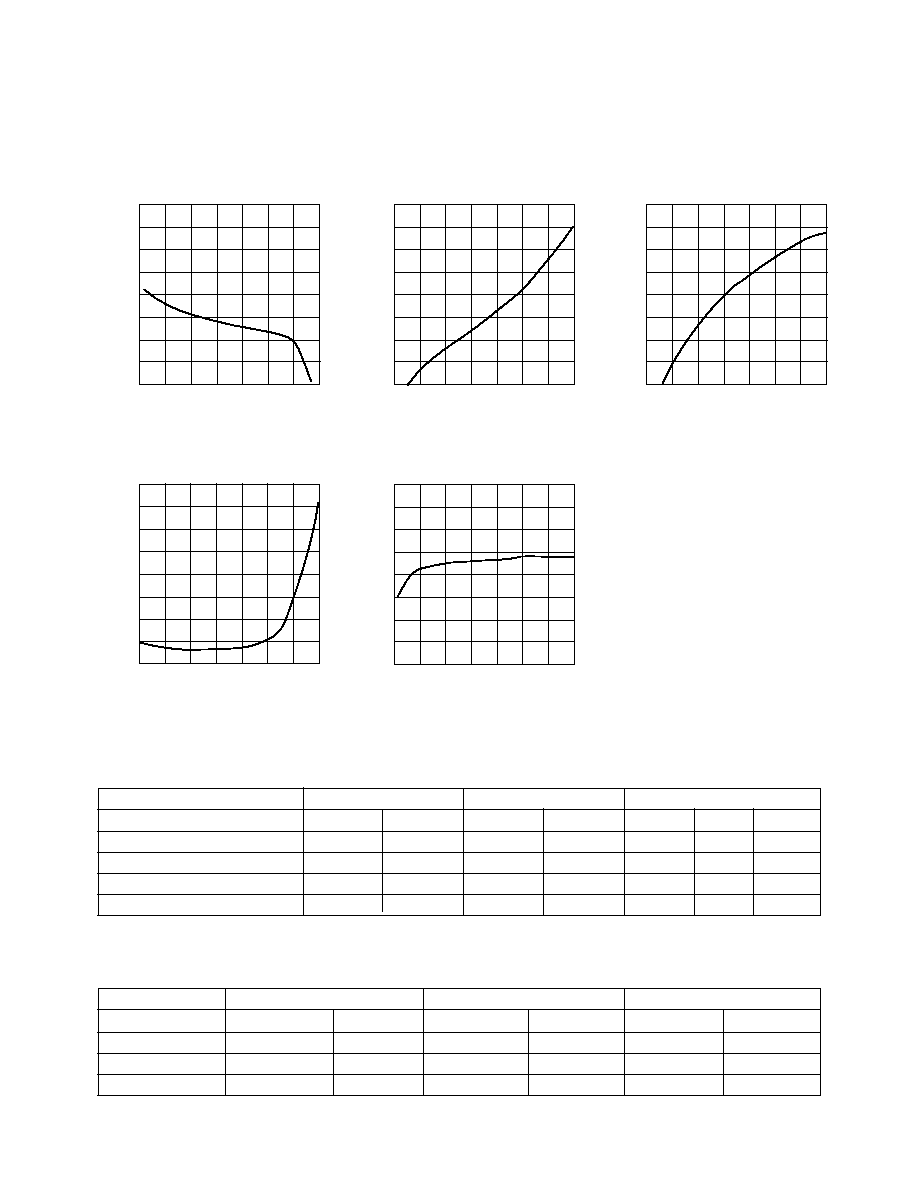
FREQUENCY (GHz)
0
-0.5
-1.0
-1.5
-2.0
INSERTION LOSS (dB)
0
1
2
3
Figure 3. Isolation vs. Frequency.
V
Control
= -5 V.
Figure 1. Insertion Loss vs. Frequency.
V
Control
= -5 V.
Figure 2. Off Port VSWR vs. Frequency.
V
Control
= -5 V.
Figure 5. Output Power vs. Frequency.
V
Control
= -7 V.
FREQUENCY (GHz)
-10
-20
-30
-40
-50
ISOLATION (dB)
0
1
2
3
FREQUENCY (GHz)
2:1
1.5:1
1:1
OFF PORT VSWR
0
1
2
3
Figure 4. On Port VSWR vs. Frequency.
V
Control
= -5 V.
FREQUENCY (GHz)
2:1
1.5:1
1:1
ON PORT VSWR
0
1
2
3
FREQUENCY (GHz)
40
30
20
10
0
P
1 dB
(dBm)
0
1
2
3
7-164
Typical Scattering Parameters,
ON Switch Port, Z
O
= 50
, T
A
= 25
°
C, V
C
= -5 V
Freq.
S
11
S
21
S
12
S
22
MHz
Mag.
Ang.
dB
Mag.
Ang.
dB
Mag.
Ang.
Mag.
Ang.
0.2
.05
-18.2
-.9
.90
-5.1
-.9
.904
-5.0
.05
-14.1
0.4
.05
-18.3
-.9
.90
-9.4
-.9
.9.6
-9.2
.04
-10.1
0.6
.05
-20.6
-.9
.90
-13.9
-.9
.898
-13.6
.03
-8.2
0.8
.05
-18.7
-.9
.90
-18.2
-.9
.898
-17.8
.02
8.9
1.0
.05
-20.4
-1.0
.89
-22.8
-1.0
.890
-22.3
.02
30.5
1.2
.06
-26.3
-1.0
.89
-27.8
-1.0
.893
-26.9
.01
42.3
1.4
.06
-29.1
-1.0
.89
-32.7
-1.0
.891
-31.5
.02
55.2
1.6
.07
-38.1
-1.1
.88
-37.5
-1.0
.889
-36.3
.02
59.1
1.8
.06
-46.4
-1.1
.88
-42.4
-1.1
.884
-41.5
.01
19.1
2.0
.06
-63.8
-1.2
.87
-47.8
-1.1
.879
-46.6
.01
-75.6
2.2
.06
-82.3
-1.2
.87
-53.5
-1.2
.871
-52.2
.03
-103.5
2.4
.07
-109.8
-1.3
.86
-58.5
-1.2
.867
-57.8
.05
-115.3
2.6
.08
-128.7
-1.4
.85
-63.2
-1.4
.851
-62.9
.08
-126.2
2.8
.11
-153.4
-1.5
.84
-68.7
-1.5
.838
-70.0
.11
-134.4
3.0
.14
-169.6
-1.6
.83
-74.0
-2.0
.791
-76.5
.16
-144.1
3.2
.20
178.3
-2.0
.79
-80.3
-2.5
.746
-82.8
.20
-152.8
3.4
.26
167.7
-2.3
.77
-83.8
-3.1
.700
-87.2
.26
-163.4
3.6
.31
154.5
-2.4
.76
-87.3
-3.3
.686
-93.8
.29
-168.1
3.8
.40
152.0
-2.5
.75
-90.3
-4.0
.632
-99.3
.37
-169.7
4.0
.51
145.4
-3.0
.71
-100.2
-4.6
.588
-99.6
.37
167.2
4.2
.63
139.5
-3.3
.68
-101.6
-5.4
.534
-101.6
.43
168.5
4.4
.82
133.0
-3.1
.70
-103.8
-6.1
.498
-104.6
.46
162.7
Typical Scattering Parameters,
OFF Switch Port, Z
O
= 50
, T
A
= 25
°
C, V
C
= -5 V
Freq.
S
11
S
21
S
12
S
22
GHz
Mag.
Ang.
dB
Mag.
Ang.
dB
Mag.
Ang.
Mag.
Ang.
0.2
.06
-9.8
-52.0
0
73.6
-46.0
.005
74.7
.01
146.5
0.4
.05
0
-42.4
.01
94.8
-41.9
.008
95.5
.03
130.7
0.6
.05
27.3
-36.4
.02
113.0
-36.5
.015
113.7
.05
125.1
0.8
.06
20.7
-35.2
.02
92.3
-35.4
.017
93.0
.07
116.9
1.0
.06
21.7
-33.7
.02
106.1
-33.6
.021
107.1
.08
115.7
1.2
.07
20.6
-31.4
.03
114.5
-32.0
.025
116.4
.10
114.8
1.4
.08
15.7
-30.5
.03
122.9
-29.1
.035
125.5
.12
114.6
1.6
.08
-5.6
-28.0
.04
112.0
-27.7
.041
114.2
.14
116.3
1.8
.08
-11.8
-26.0
.05
122.0
-26.2
.049
124.9
.16
115.2
2.0
.07
-17.0
-24.4
.06
121.9
-24.2
.062
125.4
.18
117.1
2.2
.08
-24.6
-21.9
.08
124.3
-22.3
.077
128.3
.21
118.5
2.4
.07
-40.0
-20.9
.09
119.5
-20.4
.095
123.5
.23
117.9
2.6
.06
-46.7
-20.0
.10
119.4
-19.6
.105
124.0
.25
117.8
2.8
.05
-66.2
-18.4
.12
119.0
-17.8
.129
122.9
.27
117.9
3.0
.05
-112.4
-16.5
.15
116.5
-16.1
.157
119.7
.30
118.0
3.2
.08
-158.0
-15.4
.17
111.0
-14.4
.191
113.1
.32
116.2
3.4
.16
170.2
-14.4
.19
100.7
-13.8
.204
100.3
.33
119.8
3.6
.23
158.7
-13.6
.21
100.8
-13.0
.223
96.7
.35
120.5
3.8
.34
146.0
-12.4
.24
97.3
-12.8
.229
90.9
.36
124.0
4.0
.45
138.0
-11.4
.27
83.0
-11.7
.260
78.3
.33
113.0
4.2
.54
129.9
-12.0
.25
82.7
-12.6
.234
78.8
.39
120.7
4.4
.65
125.4
-10.8
.29
81.1
-11.9
.253
74.5
.39
116.1
7-165
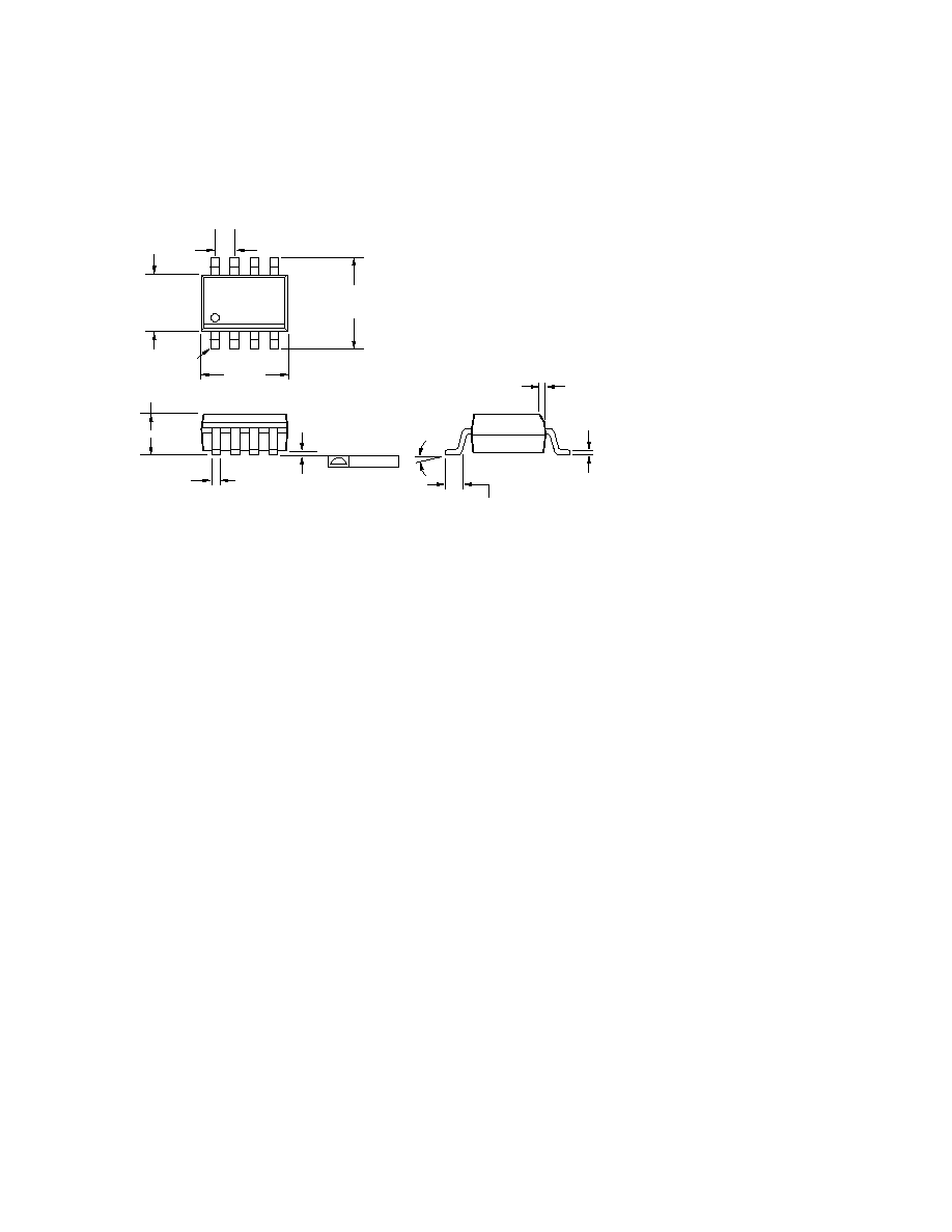
SO-8 Package Dimensions
5.84/6.20
(.230/.244)
3.80/4.00
(.1497/.1574)
Pin 1
1.27 (.050)
6x
4.72/5.00
(.186/.197)
0.10/0.25
(.004/.0098)
0.33/0.51
(.013/.020) 8X
1.35/1.75
(.0532/.0688)
0.19/0.25
(.0075/.0098)
0.41/1.27
(.016/.050)
0
°
/8
°
0.38
±
0.10
(.015
±
.004) x 45
°
0.10 (.004)
Note:
1. Dimensions are shown in millimeters (inches).
Document Outline
- List of Figures
- 1. Insertion Loss vs. Frequency.
- 2. Off Port VSWR vs. Frequency.
- 3. Isolation vs. Frequency.
- 4. On Port VSWR vs. Frequency.
- 5. Output Power vs. Frequency.
- Features
- Description
- SO-8 Package
- AC Equivalent Circuit/Pinout
- MGS-71008 Absolute Maximum Ratings
- Electrical Specifications, TA = 25°C
- MGS-70008 Typical Performance, TA = 25°C
- MGS-71008 Truth Table
- MGS-71008 Typical Power Performance vs. Frequency and Control Voltage (VC )
- Typical Scattering Parameters
- Typical Scattering Parameters
- SO-8 Package Dimensions