 | –≠–ª–µ–∫—Ç—Ä–æ–Ω–Ω—ã–π –∫–æ–º–ø–æ–Ω–µ–Ω—Ç: MSA-0100 | –°–∫–∞—á–∞—Ç—å:  PDF PDF  ZIP ZIP |
Document Outline
- List of Figures
- 1. Typical Power Gain vs. Frequency
- 2. Power Gain vs. Current
- 3. Output Power at 1 dB Gain Compression, NF and Power Gain vs. Mounting Surface Temperature
- 4. Output Power at 1 dB Gain Compression vs.Frequency
- 5. Noise Figure vs. Frequency
- Features
- Description
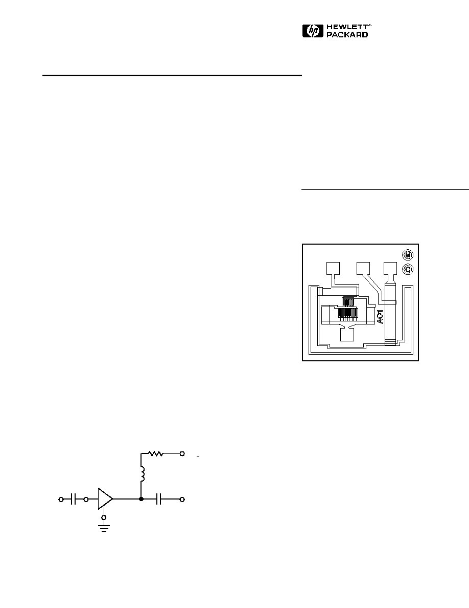
- Typical Biasing Configuration
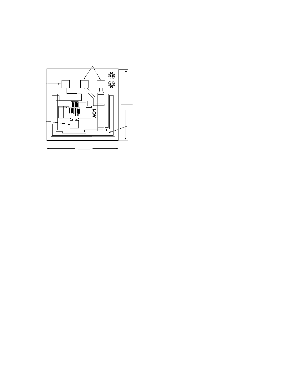
- Chip Outline
- MSA-0100 Absolute Maximum Ratings
- Electrical Specifications
- Part Number Ordering Information
- MSA-0100 Typical Scattering Parameters
- MSA-0100 Typical Performance
- MSA-0100 Chip Dimensions
6-242
Cascadable Silicon Bipolar
MMIC Amplifier
Technical Data
Features
∑ Cascadable 50
Gain Block
∑ 3 dB Bandwidth:
DC to 1.3 GHz
∑ High Gain:
18.5 dB Typical at 0.5 GHz
∑ Unconditionally Stable
(k>1)
MSA-0100
Chip Outline
[1]
Typical Biasing Configuration
C
block
C
block
R
bias
V
CC
>
7 V
V
d
= 5 V
RFC (Optional)
IN
OUT
MSA
Note:
1. This chip contains additional biasing
options. The performance specified
applies only to the bias option whose
bond pads are indicated on the chip
outline. Refer to the APPLICATIONS
section "Silicon MMIC Chip Use" for
additional information.
Description
The MSA-0100 is a high performance
silicon bipolar Monolithic Microwave
Integrated Circuit (MMIC) chip. This
MMIC is designed for use as a general
purpose 50
gain block. Typical
applications include narrow and
broad band IF and RF amplifiers in
commercial, industrial and military
applications.
The MSA-series is fabricated using
HP's 10 GHz f
T
, 25 GHz f
MAX
, silicon
bipolar MMIC process which uses
nitride self-alignment, ion implanta-
tion, and gold metallization to
achieve excellent performance,
uniformity and reliability. The use
of an external bias resistor for
temperature and current stability
also allows bias flexibility.
The recommended assembly
procedure is gold-eutectic die
attach at 400
∞
C and either wedge or
ball bonding using 0.7 mil gold
wire.
[1]
See APPLICATIONS section,
"Chip Use".
5965-9689E

6-243
MSA-0100 Absolute Maximum Ratings
Parameter
Absolute Maximum
[1]
Device Current
40 mA
Power Dissipation
[2,3]
200 mW
RF Input Power
+20 dBm
Junction Temperature
200
∞
C
Storage Temperature
≠65 to 200
∞
C
Thermal Resistance
[2,4]
:
jc
= 45
∞
C/W
Part Number Ordering Information
Part Number
Devices Per Tray
MSA-0100-GP4
100
G
P
Power Gain (|S
21
|
2
)
f = 0.1 GHz
dB
19.0
G
P
Gain Flatness
f = 0.1 to 0.7 GHz
dB
±
0.6
f
3 dB
3 dB Bandwidth
GHz
1.3
Input VSWR
f = 0.1 to 3.0 GHz
1.3:1
Output VSWR
f = 0.1 to 3.0 GHz
1.3:1
NF
50
Noise Figure
f = 0.5 GHz
dB
5.5
P
1 dB
Output Power at 1 dB Gain Compression
f = 0.5 GHz
dBm
1.5
IP
3
Third Order Intercept Point
f = 0.5 GHz
dBm
14.0
t
D
Group Delay
f = 0.5 GHz
psec
150
V
d
Device Voltage
V
4.5
5.0
5.5
dV/dT
Device Voltage Temperature Coefficient
mV/
∞
C
≠9.0
Notes:
1. The recommended operating current range for this device is 13 to 25 mA. Typical performance as a function of current
is on the following page.
2. RF performance of the chip is determined by packaging and testing 10 devices per wafer in a dual ground configuration.
Electrical Specifications
[1]
, T
A
= 25
∞
C
Symbol
Parameters and Test Conditions
[2]
: I
d
= 17 mA, Z
O
= 50
Units
Min.
Typ.
Max.
VSWR
Notes:
1. Permanent damage may occur if any of these limits are exceeded.
2. T
Mounting Surface
(T
MS
)
= 25
∞
C.
3. Derate at 22.2 mW/
∞
C for T
MS
> 191
∞
C.
4. The small spot size of this technique results in a higher, though more
accurate determination of
jc
than do alternate methods. See MEASURE-
MENTS section "Thermal Resistance" for more information.
6-244
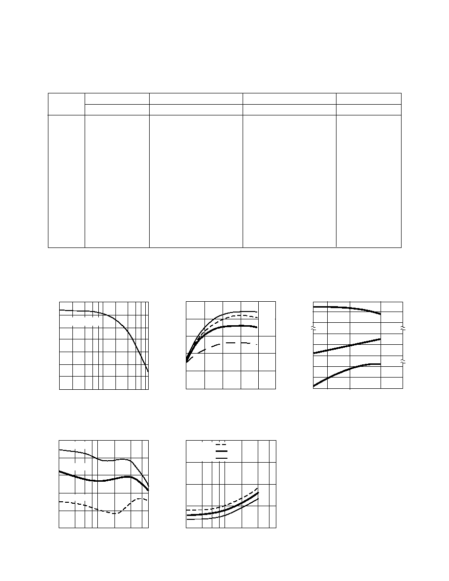
MSA-0100 Typical Performance, T
A
= 25
∞
C
(unless otherwise noted)
≠2
0
2
4
6
8
16
18
20
6
≠55
≠25
+25
+85
+125
8
4
P
1 dB
(dBm)
NF (dB)
G
P
P
1 dB
NF
G
p
(dB)
0.1
0.3 0.5
1.0
3.0
6.0
FREQUENCY (GHz)
Figure 1. Typical Power Gain vs.
Frequency, T
A
= 25
∞
C, I
d
= 17 mA.
I
d
(mA)
Figure 2. Power Gain vs. Current.
0
5
10
15
20
25
0
3
6
9
12
15
18
21
G
p
(dB)
G
p
(dB)
10
20
25
30
15
TEMPERATURE (
∞
C)
Figure 3. Output Power at 1 dB Gain
Compression, NF and Power Gain vs.
Mounting Surface Temperature,
f = 0.5 GHz, I
d
= 17 mA.
0.1 GHz
1.0 GHz
2.0 GHz
5.0
5.5
6.0
6.5
7.0
NF (dB)
FREQUENCY (GHz)
Figure 5. Noise Figure vs. Frequency.
0.1
0.2 0.3
0.5
2.0
1.0
4.0
0.1
0.2 0.3
0.5
2.0
1.0
FREQUENCY (GHz)
Figure 4. Output Power at 1 dB Gain
Compression vs. Frequency.
≠4
≠2
0
2
4
6
P
1 dB
(dBm)
Gain Flat to DC
0.5 GHz
I
d
= 20 mA
I
d
= 17 mA
I
d
= 13 mA
I
d
= 13 mA
I
d
= 17 mA
I
d
= 20 mA
MSA-0100 Typical Scattering Parameters
[1]
(Z
O
= 50
, T
A
= 25
∞
C, I
d
= 17 mA)
Freq.
GHz
Mag
Ang
dB
Mag
Ang
dB
Mag
Ang
Mag
Ang
0.1
.08
171
19.0
8.91
174
≠22.7
.073
2
.10
≠11
0.2
.07
161
18.9
8.82
169
≠22.5
.075
6
.11
≠24
0.3
.07
152
18.8
8.72
163
≠22.3
.077
9
.10
≠35
0.4
.06
143
18.6
8.56
156
≠22.4
.076
12
.11
≠44
0.5
.06
133
18.5
8.37
151
≠22.1
.079
14
.11
≠53
0.6
.05
115
18.2
8.15
146
≠21.9
.080
19
.12
≠60
0.8
.04
84
17.7
7.68
136
≠21.3
.086
22
.12
≠75
1.0
.04
3
17.1
7.17
126
≠20.3
.096
26
.12
≠88
1.5
.08
≠39
15.5
5.95
106
≠19.3
.109
32
.10
≠107
2.0
.12
≠76
13.7
4.86
90
≠17.9
.127
32
.08
≠128
2.5
.15
≠102
12.2
4.09
82
≠16.9
.142
36
.06
≠130
3.0
.19
≠122
10.8
3.47
71
≠16.4
.151
36
.06
≠125
3.5
.25
≠137
9.4
2.96
60
≠15.6
.165
34
.07
≠107
4.0
.27
≠147
8.2
2.56
51
≠15.2
.173
32
.10
≠86
4.5
.28
≠157
7.0
2.24
42
≠14.8
.182
29
.13
≠80
5.0
.28
≠171
6.0
2.00
35
≠14.4
.190
28
.16
≠77
Note:
1. S-parameters are de-embedded from 70 mil package measured data using the package model found in the DEVICE
MODELS section.
S
11
S
21
S
12
S
22
6-245
MSA-0100 Chip Dimensions
NOT APPLICABLE
INPUT
GROUND
OPTIONAL
OUTPUT
[1]
394
µ
m
15.5 mil
394
µ
m
15.5 mil
Chip thickness is 114
µ
m/4.5 mil. Bond Pads are
41
µ
m/1.6 mil typical on each side.
Note 1: Output contact is made by die attaching
the backside of the die.