 | –≠–ª–µ–∫—Ç—Ä–æ–Ω–Ω—ã–π –∫–æ–º–ø–æ–Ω–µ–Ω—Ç: MSA-0135 | –°–∫–∞—á–∞—Ç—å:  PDF PDF  ZIP ZIP |
Document Outline
- List of Figures
- 1. Typical Power Gain vs. Frequency
- 2. Device Current vs. Voltage
- 3. Power Gain vs. Current
- 4. Output Power at 1 dB Gain Compression, NF and Power Gain vs. CaseTemperature
- 5. Output Power at 1 dB Gain Compression vs. Frequency
- 6. Noise Figure vs. Frequency
- Features
- Description
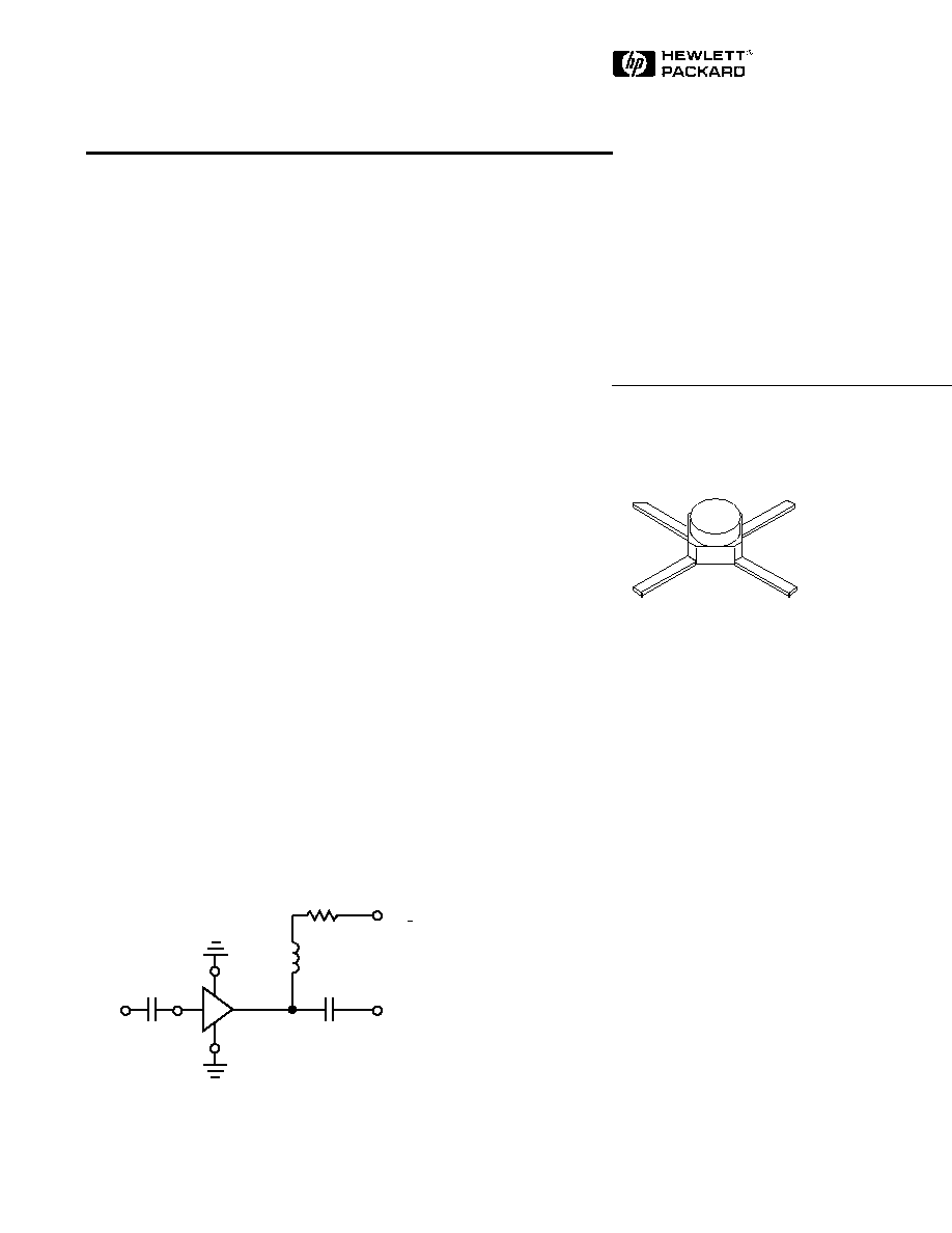
- Typical Biasing Configuration
- 35 micro-X Package
- MSA-0135, -0136 Absolute Maximum Ratings
- MSA-0135, -0136 Electrical Specifications
- MSA-0135, -0136 Typical Scattering Parameters
- MSA-0135, -0136 Typical Performance
- 35 micro-X Package Dimensions
6-250
Cascadable Silicon Bipolar
MMIC Amplifiers
Technical Data
Features
∑ Cascadable 50
Gain Block
∑ 3 dB Bandwidth:
DC to 1.2 GHz
∑ High Gain:
18.5 dB Typical at 0.5 GHz
∑ Unconditionally Stable
(k>1)
∑ Cost Effective Ceramic
Microstrip Package
MSA-0135, -0136
35 micro-X Package
[1]
Description
The MSA-0135 is a high perfor-
mance silicon bipolar Monolithic
Microwave Integrated Circuit
(MMIC) housed in a cost effective,
microstrip package. This MMIC is
designed for use as a general
Typical Biasing Configuration
C
block
C
block
R
bias
V
CC
>
7 V
V
d
= 5 V
RFC (Optional)
IN
OUT
MSA
4
1
2
3
Note:
1.
Short leaded 36 package available
upon request.
purpose 50
gain block. Typical
applications include narrow and
broad band IF and RF amplifiers
in industrial and military applica-
tions.
The MSA-series is fabricated using
HP's 10 GHz f
T
, 25 GHz f
MAX
,
silicon bipolar MMIC process
which uses nitride self-alignment,
ion implantation, and gold metalli-
zation to achieve excellent
performance, uniformity and
reliability. The use of an external
bias resistor for temperature and
current stability also allows bias
flexibility.
Available in cut lead version
(package 36) as MSA-0136.
5965-9691E
6-251
MSA-0135, -0136 Absolute Maximum Ratings
Parameter
Absolute Maximum
[1]
Device Current
40 mA
Power Dissipation
[2,3]
200 mW
RF Input Power
+13 dBm
Junction Temperature
200
∞
C
Storage Temperature
≠65 to 200
∞
C
Thermal Resistance
[2,5]
:
jc
= 150
∞
C/W
Notes:
1. Permanent damage may occur if any of these limits are exceeded.
2. T
CASE
= 25
∞
C.
3. Derate at 6.7 mW/
∞
C for T
C
> 170
∞
C.
4. Storage above +150
∞
C may tarnish the leads of this package making it difficult to solder into a circuit.
5. The small spot size of this technique results in a higher, though more accurate determination of
jc
than do alternate
methods. See MEASUREMENTS section "Thermal Resistance" for more information.
G
P
Power Gain (|S
21
|
2
)
f = 0.1 GHz
dB
18.0
19.0
G
P
Gain Flatness
f = 0.1 to 0.6 GHz
dB
±
0.6
f
3 dB
3 dB Bandwidth
GHz
1.2
Input VSWR
f = 0.1 to 3.0 GHz
1.3:1
Output VSWR
f = 0.1 to 3.0 GHz
1.3:1
NF
50
Noise Figure
f = 0.5 GHz
dB
5.5
P
1 dB
Output Power at 1 dB Gain Compression
f = 0.5 GHz
dBm
1.5
IP
3
Third Order Intercept Point
f = 0.5 GHz
dBm
14.0
t
D
Group Delay
f = 0.5 GHz
psec
160
V
d
Device Voltage
V
4.5
5.0
5.5
dV/dT
Device Voltage Temperature Coefficient
mV/
∞
C
≠9.0
Notes:
1. The recommended operating current range for this device is 13 to 25 mA. Typical performance as a function of current
is on the following page.
MSA-0135, -0136 Electrical Specifications
[1]
, T
A
= 25
∞
C
Symbol
Parameters and Test Conditions: I
d
= 17 mA, Z
O
= 50
Units
Min.
Typ.
Max.
VSWR
6-252
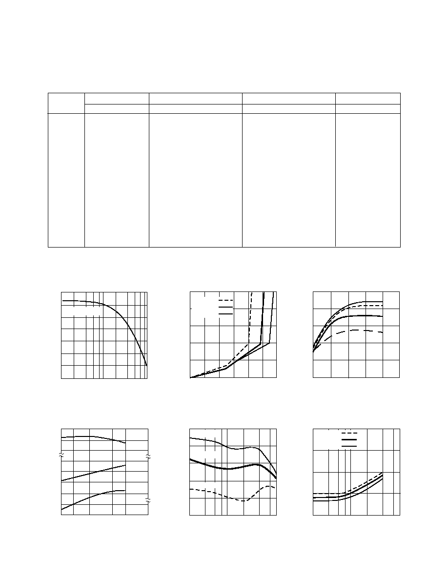
MSA-0135, -0136 Typical Performance, T
A
= 25
∞
C
(unless otherwise noted)
≠2
0
4
2
6
8
16
18
20
4
≠55
≠25
+25
+85
+125
6
8
2
P
1 dB
(dBm)
NF (dB)
G
P
P
1 dB
NF
G
p
(dB)
0.1
0.3 0.5
1.0
3.0
6.0
FREQUENCY (GHz)
Figure 1. Typical Power Gain vs.
Frequency, T
A
= 25
∞
C, I
d
= 17 mA.
I
d
(mA)
Figure 3. Power Gain vs. Current.
0
5
10
15
20
25
0
3
6
9
12
15
18
21
G
p
(dB)
G
p
(dB)
10
20
25
30
15
TEMPERATURE (
∞
C)
Figure 4. Output Power at 1 dB Gain
Compression, NF and Power Gain vs.
CaseTemperature, f = 0.5 GHz, I
d
= 17 mA.
0.1 GHz
1.0 GHz
2.0 GHz
5.0
5.5
6.0
6.5
7.0
NF (dB)
FREQUENCY (GHz)
Figure 6. Noise Figure vs. Frequency.
0.1
0.2 0.3
0.5
2.0
1.0
4.0
0.1
0.2 0.3
0.5
2.0
1.0
4.0
FREQUENCY (GHz)
Figure 5. Output Power at 1 dB Gain
Compression vs. Frequency.
≠4
≠2
0
2
4
6
P
1 dB
(dBm)
Gain Flat to DC
0.5 GHz
V
d
(V)
Figure 2. Device Current vs. Voltage.
0
5
10
15
20
25
I
d
(mA)
0
2
3
4
5
6
1
I
d
= 20 mA
I
d
= 17 mA
I
d
= 13 mA
T
C
= +125
∞
C
T
C
= +25
∞
C
T
C
= ≠55
∞
C
I
d
= 13 mA
I
d
= 17 mA
I
d
= 20 mA
MSA-0135, -0136 Typical Scattering Parameters (Z
O
= 50
, T
A
= 25
∞
C, I
d
= 17 mA)
Freq.
GHz
Mag
Ang
dB
Mag
Ang
dB
Mag
Ang
Mag
Ang
0.1
.08
158
19.1
9.01
172
≠23.0
.071
3
.07
≠2
0.2
.08
134
18.9
8.84
165
≠22.4
.076
6
.07
≠10
0.3
.08
116
18.7
8.65
157
≠22.5
.075
12
.07
≠10
0.4
.08
97
18.5
8.40
150
≠22.2
.078
13
.07
≠15
0.5
.09
83
18.2
8.13
143
≠21.7
.082
16
.07
≠17
0.6
.09
68
17.9
7.84
136
≠21.6
.083
17
.07
≠21
0.8
.11
47
17.2
7.25
125
≠20.7
.092
22
.07
≠30
1.0
.11
27
16.5
6.64
113
≠19.9
.101
23
.07
≠34
1.5
.11
≠18
14.6
5.37
90
≠18.3
.122
27
.06
≠34
2.0
.09
≠62
12.8
4.38
70
≠16.8
.144
24
.05
≠39
2.5
.08
≠114
11.3
3.67
58
≠16.1
.157
24
.03
≠61
3.0
.12
≠158
10.0
3.15
43
≠15.0
.177
20
.03
≠67
3.5
.18
178
8.7
2.72
28
≠14.5
.189
14
.05
≠88
4.0
.21
163
7.5
2.37
15
≠14.0
.200
9
.10
≠92
4.5
.23
145
6.4
2.10
2
≠13.4
.213
4
.14
≠99
5.0
.27
125
5.5
1.88
≠10
≠13.2
.220
≠2
.15
≠102
A model for this device is available in the DEVICE MODELS section.
S
11
S
21
S
12
S
22
6-253
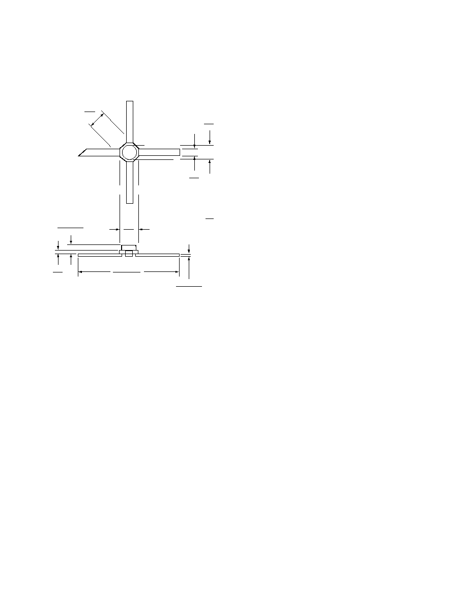
35 micro-X Package Dimensions
1
3
4
2
GROUND
DIA.
GROUND
RF OUTPUT
AND BIAS
RF INPUT
.085
2.15
.083
2.11
.020
.508
.100
2.54
.455
±
.030
11.54
±
.75
.006
±
.002
.15
±
.05
Notes:
(unless otherwise specified)
1. Dimensions are in
2. Tolerances
in .xxx =
±
0.005
mm .xx =
±
0.13
mm
.022
.56
.057
±
.010
1.45
±
.25
A01