 | –≠–ª–µ–∫—Ç—Ä–æ–Ω–Ω—ã–π –∫–æ–º–ø–æ–Ω–µ–Ω—Ç: MSA-0735 | –°–∫–∞—á–∞—Ç—å:  PDF PDF  ZIP ZIP |
Document Outline
- List of Figures
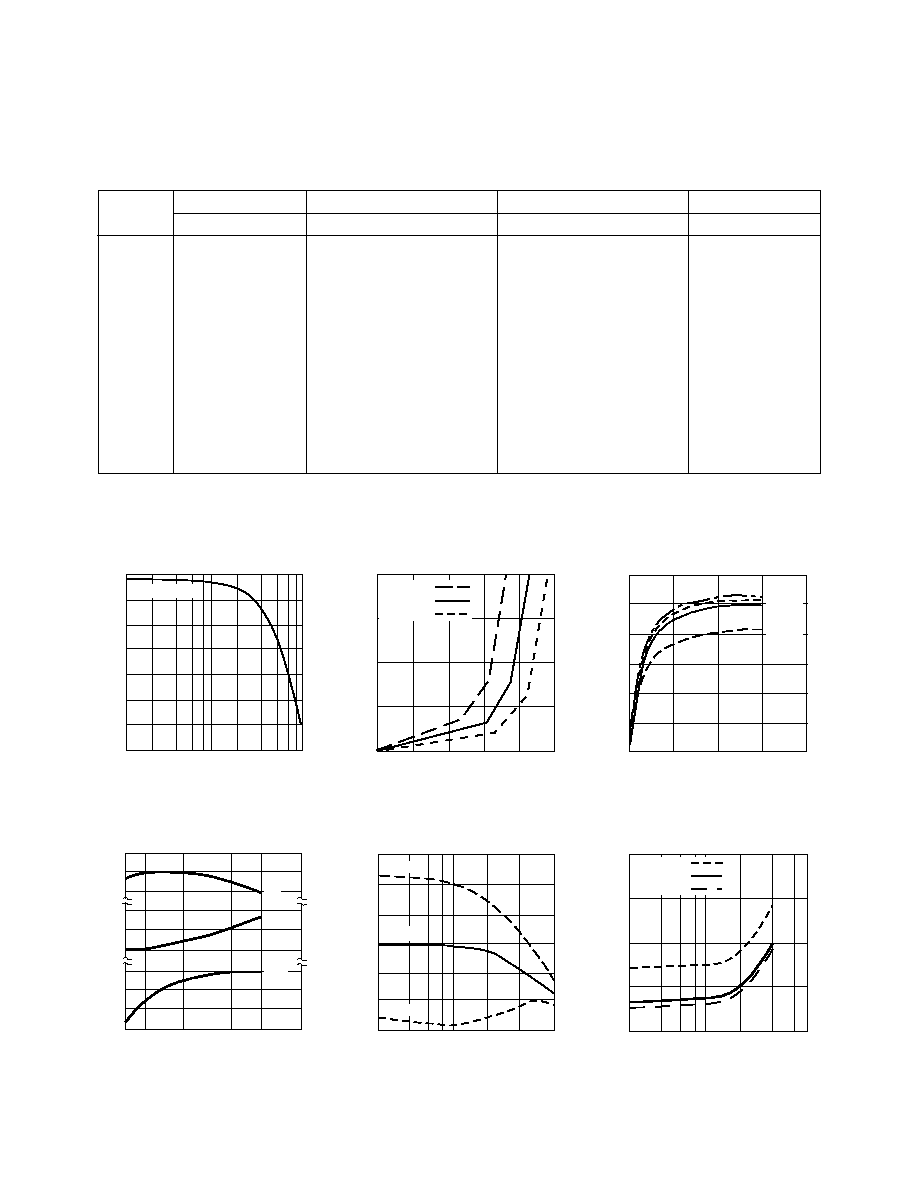
- 1. Typical Power Gain vs. Frequency
- 2. Device Current vs. Voltage
- 3. Power Gain vs. Current
- 4. Output Power at 1 dB Gain Compression, NF and Power Gain vs. Case Temperature
- 5. Output Power at 1 dB Gain Compression vs. Frequency
- 6. Noise Figure vs. Frequency
- Features
- Description
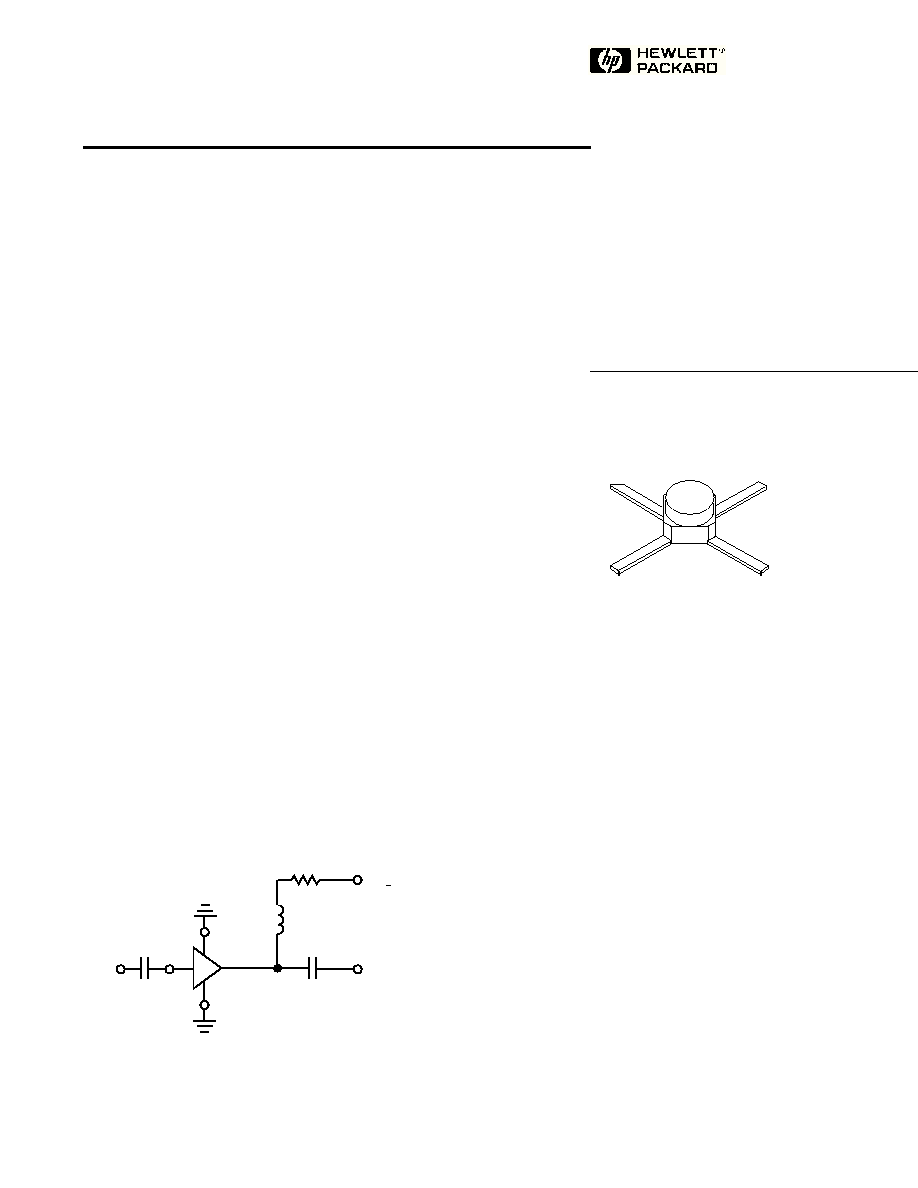
- Typical Biasing Configuration
- 35 micro-X Package
- MSA-0753, -0736 Absolute Maximum Ratings
- Electrical Specifications
- Part Number Ordering Information
- MSA-0735, -0736 Typical Scattering Parameters
- Typical Performance
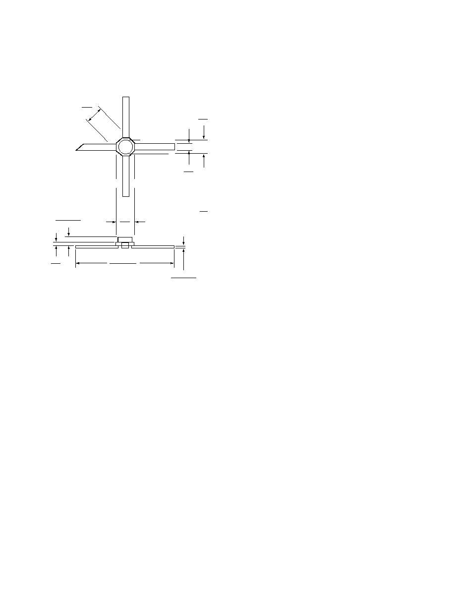
- 35 micro-X Package Dimensions
6-394
Cascadable Silicon Bipolar
MMIC Amplifiers
Technical Data
Features
∑ Cascadable 50
Gain Block
∑ Low Operating Voltage:
4.0 V Typical V
d
∑ 3 dB Bandwidth:
DC to 2.4 GHz
∑ 13.0 dB Typical Gain at
1.0 GHz
∑ Unconditionally Stable
(k>1)
∑ Cost Effective Ceramic
Microstrip Package
MSA-0735, -0736
35 micro-X Package
[1]
Description
The MSA-0735 is a high perfor-
mance silicon bipolar Monolithic
Microwave Integrated Circuit
(MMIC) housed in a cost effective,
Typical Biasing Configuration
Note:
1. Short leaded 36 package available upon
request.
C
block
C
block
R
bias
V
CC
>
5 V
V
d
= 4.0 V
RFC (Optional)
IN
OUT
MSA
4
1
2
3
microstrip package. This MMIC is
designed for use as a general
purpose 50
gain block. Typical
applications include narrow and
broad band IF and RF amplifiers
in industrial and military applica-
tions.
The MSA-series is fabricated using
HP's 10 GHz f
T
, 25 GHz f
MAX
,
silicon bipolar MMIC process
which uses nitride self-alignment,
ion implantation, and gold metalli-
zation to achieve excellent
performance, uniformity and
reliability. The use of an external
bias resistor for temperature and
current stability also allows bias
flexibility.
5965-9591E
6-395
MSA-0735, -0736 Absolute Maximum Ratings
Parameter
Absolute Maximum
[1]
Device Current
60 mA
Power Dissipation
[2,3]
275 mW
RF Input Power
+13 dBm
Junction Temperature
200
∞
C
Storage Temperature
≠65 to 200
∞
C
Thermal Resistance
[2,5]
:
jc
= 155
∞
C/W
Notes:
1. Permanent damage may occur if any of these limits are exceeded.
2. T
CASE
= 25
∞
C.
3. Derate at 6.5 mW/
∞
C for T
C
> 157
∞
C.
4. Storage above +150
∞
C may tarnish the leads of this package making it
difficult to solder into a circuit.
5. Ths small spot size of this technique results in a higher, though more
accurate determination of
jc
than do alternate methods. See MEASURE-
MENTS section "Thermal Resistance" for more information.
G
P
Power Gain (|S
21
|
2
)
f = 0.1 GHz
dB
12.5
13.5
14.5
G
P
Gain Flatness
f = 0.1 to 1.3 GHz
dB
±
0.6
±
1.0
f
3 dB
3 dB Bandwidth
GHz
2.4
Input VSWR
f = 0.1 to 2.5 GHz
2.0:1
Output VSWR
f = 0.1 to 2.5 GHz
1.8:1
NF
50
Noise Figure
f = 1.0 GHz
dB
4.5
P
1 dB
Output Power at 1 dB Gain Compression
f = 1.0 GHz
dBm
5.5
IP
3
Third Order Intercept Point
f = 1.0 GHz
dBm
19.0
t
D
Group Delay
f = 1.0 GHz
psec
140
V
d
Device Voltage
V
3.6
4.0
4.4
dV/dT
Device Voltage Temperature Coefficient
mV/
∞
C
≠7.0
Note:
1. The recommended operating current range for this device is 15 to 40 mA. Typical performance as a function of current
is on the following page.
Electrical Specifications
[1]
, T
A
= 25
∞
C
Symbol
Parameters and Test Conditions: I
d
= 22 mA, Z
O
= 50
Units
Min.
Typ.
Max.
VSWR
Part Number Ordering Information
Part Number
No. of Devices
Container
MSA-0735
10
Strip
MSA-0736-BLK
100
Antistatic Bag
MSA-0736-TR1
1000
7" Reel
For more information, see "Tape and Reel Packaging for Semiconductor Devices".
6-396
MSA-0735, -0736 Typical Scattering Parameters (Z
O
= 50
, T
A
= 25
∞
C, I
d
= 22 mA)
Freq.
GHz
Mag
Ang
dB
Mag
Ang
dB
Mag
Ang
Mag
Ang
0.1
.13
≠3
13.5
4.71
175
≠19.0
.112
2
.29
≠7
0.2
.13
≠6
13.4
4.69
170
≠18.5
.119
3
.29
≠12
0.4
.14
≠13
13.4
4.68
160
≠18.6
.118
6
.29
≠24
0.6
.16
≠20
13.3
4.64
150
≠18.4
.120
7
.28
≠35
0.8
.19
≠29
13.2
4.60
140
≠18.1
.125
8
.28
≠47
1.0
.21
≠40
12.9
4.42
129
≠17.6
.131
10
.27
≠58
1.5
.27
≠71
12.2
4.07
104
≠16.5
.149
10
.24
≠83
2.0
.32
≠107
11.5
3.74
79
≠15.6
.165
7
.19
≠103
2.5
.37
≠134
10.3
3.26
62
≠15.3
.173
5
.15
≠113
3.0
.43
≠160
8.8
2.76
44
≠15.4
.171
0
.14
≠120
3.5
.47
≠179
7.5
2.37
27
≠15.3
.173
≠4
.16
≠120
4.0
.49
167
6.2
2.05
12
≠15.2
.168
≠6
.21
≠121
5.0
.51
134
4.0
1.59
≠15
≠15.2
.173
≠11
.28
≠135
6.0
.60
96
2.1
1.27
≠42
≠14.6
.185
≠16
.29
≠167
A model for this device is available in the DEVICE MODELS section.
S
11
S
21
S
12
S
22
G
p
(dB)
0.1
0.3 0.5
1.0
3.0
6.0
FREQUENCY (GHz)
Figure 1. Typical Power Gain vs.
Frequency, I
d
= 22 mA.
1
0
2
3
4
5
V
d
(V)
Figure 2. Device Current vs. Voltage.
Figure 3. Power Gain vs. Current.
0
2
4
6
8
10
12
14
0
10
20
30
40
Gain Flat to DC
I
d
(mA)
T
C
= +125
∞
C
T
C
= +25
∞
C
T
C
= ≠55
∞
C
I
d
(mA)
G
p
(dB)
4
6
8
10
12
16
14
10
20
30
40
0.1 GHz
0.5 GHz
1.0 GHz
2.0 GHz
3
4
5
6
12
13
14
≠25
≠55
+25
+85
+125
4
5
6
P
1 dB
(dBm)
NF (dB)
NF
G
p
(dB)
TEMPERATURE (
∞
C)
Figure 4. Output Power at 1 dB Gain
Compression, NF and Power Gain vs.
Case Temperature, f = 1.0 GHz,
I
d
=22mA.
0.1
0.2 0.3
0.5
2.0
1.0
4.0
FREQUENCY (GHz)
Figure 5. Output Power at 1 dB Gain
Compression vs. Frequency.
≠3
0
3
6
9
12
15
P
1 dB
(dBm)
I
d
= 40 mA
I
d
= 15 mA
I
d
= 22 mA
4.5
4.0
5.0
5.5
6.0
NF (dB)
FREQUENCY (GHz)
Figure 6. Noise Figure vs. Frequency.
0.1
0.2 0.3
0.5
2.0
1.0
P
1 dB
G
P
I
d
= 15 mA
I
d
= 22 mA
I
d
= 40 mA
Typical Performance, T
A
= 25
∞
C
(unless otherwise noted)
6-397
35 micro-X Package Dimensions
1
3
4
2
GROUND
DIA.
GROUND
RF OUTPUT
AND BIAS
RF INPUT
.085
2.15
.083
2.11
.020
.508
.100
2.54
.455
±
.030
11.54
±
.75
.006
±
.002
.15
±
.05
Notes:
(unless otherwise specified)
1. Dimensions are in
2. Tolerances
in .xxx =
±
0.005
mm .xx =
±
0.13
mm
.022
.56
.057
±
.010
1.45
±
.25
A07