 | –≠–ª–µ–∫—Ç—Ä–æ–Ω–Ω—ã–π –∫–æ–º–ø–æ–Ω–µ–Ω—Ç: MSA-0886 | –°–∫–∞—á–∞—Ç—å:  PDF PDF  ZIP ZIP |
Document Outline
- List of Figures
- 1. Typical Power Gain vs. Frequency
- 2. Device Current vs. Voltage
- 3. Output Power at 1 dB Gain Compression, NF and Power Gain vs. Case Temperature
- 4. Output Power at 1 dB Gain Compression vs. Frequency
- 5. Noise Figure vs. Frequency
- Features
- Typical Biasing Configuration
- Description
- 86 Plastic Package
- MSA-0886 Absolute Maximum Ratings
- Electrical Specifications
- Part Number Ordering Information
- MSA-0886 Typical Scattering Parameters
- Typical Performance
- 86 Plastic Package Dimensions
6-426
Cascadable Silicon Bipolar
MMIC Amplifier
Technical Data
Features
∑ Usable Gain to 5.5 GHz
∑ High Gain:
32.5 dB Typical at 0.1 GHz
22.5 dB Typical at 1.0 GHz
∑ Low Noise Figure:
3.3 dB Typical at 1.0 GHz
∑ Surface Mount Plastic
Package
∑ Tape-and-Reel Packaging
Option Available
[1]
MSA-0886
86 Plastic Package
Description
The MSA-0886 is a high perfor-
mance silicon bipolar Monolithic
Microwave Integrated Circuit
(MMIC) housed in a low cost,
surface mount plastic package.
This MMIC is designed for use as a
general purpose 50
gain block
above 0.5 GHz and can be used as
a high gain transistor below this
frequency. Typical applications
include narrow and moderate band
IF and RF amplifiers in commer-
cial and industrial applications.
The MSA-series is fabricated using
HP's 10 GHz f
T
, 25 GHz f
MAX
,
silicon bipolar MMIC process
which uses nitride self-alignment,
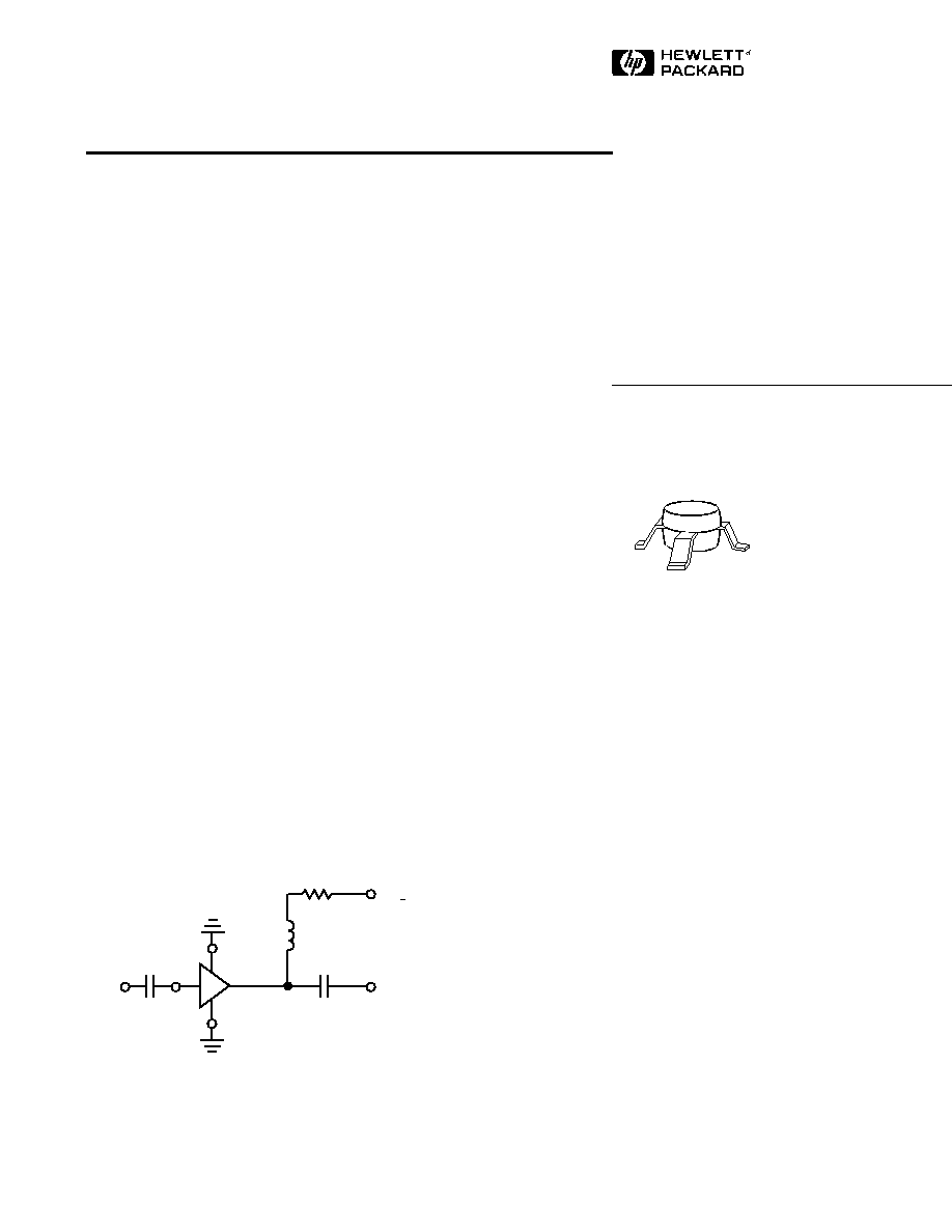
Typical Biasing Configuration
C
block
C
block
R
bias
V
CC
>
10
V
V
d
= 7.8 V
RFC (Optional)
IN
OUT
MSA
4
1
2
3
Note:
1. Refer to PACKAGING section "Tape-
and-Reel Packaging for Semiconduc-
tor Devices."
ion implantation, and gold metalli-
zation to achieve excellent perfor-
mance, uniformity and reliability.
The use of an external bias resistor
for temperature and current
stability also allows bias flexibility.
5965-9547E
6-427
MSA-0886 Absolute Maximum Ratings
Parameter
Absolute Maximum
[1]
Device Current
65 mA
Power Dissipation
[2,3]
500 mW
RF Input Power
+13 dBm
Junction Temperature
150
∞
C
Storage Temperature
≠65
∞
C to 150
∞
C
Thermal Resistance
[2,4]
:
jc
= 140
∞
C/W
Notes:
1. Permanent damage may occur if any of these limits are exceeded.
2. T
CASE
= 25
∞
C.
3. Derate at 7.1 mW/
∞
C for T
C
> 80
∞
C.
4. See MEASUREMENTS section "Thermal Resistance" for more information.
G
P
Power Gain (|S
21
|
2
)
f = 0.1 GHz
dB
32.5
f = 1.0 GHz
20.5
22.5
Input VSWR
f = 0.1 to 3.0 GHz
2.1:1
Output VSWR
f = 0.1 to 3.0 GHz
1.9:1
NF
50
Noise Figure
f = 1.0 GHz
dB
3.3
P
1 dB
Output Power at 1 dB Gain Compression
f = 1.0 GHz
dBm
12.5
IP
3
Third Order Intercept Point
f = 1.0 GHz
dBm
27.0
t
D
Group Delay
f = 1.0 GHz
psec
140
V
d
Device Voltage
V
6.2
7.8
9.4
dV/dT
Device Voltage Temperature Coefficient
mV/
∞
C
≠17.0
Note:
1. The recommended operating current range for this device is 20 to 40 mA. Typical performance as a function of current
is on the following page.
Electrical Specifications
[1]
, T
A
= 25
∞
C
Symbol
Parameters and Test Conditions: I
d
= 36 mA, Z
O
= 50
Units
Min.
Typ.
Max.
VSWR
Part Number Ordering Information
Part Number
No. of Devices
Container
MSA-0886-TR1
1000
7" Reel
MSA-0886-BLK
100
Antistatic Bag
For more information, see "Tape and Reel Packaging for Semiconductor Devices".
6-428
MSA-0886 Typical Scattering Parameters
[1]
(Z
O
= 50
, T
A
= 25
∞
C, I
d
= 36 mA)
Freq.
GHz
Mag
Ang
dB
Mag
Ang
dB
Mag
Ang
Mag
Ang
k
0.1
.63
≠22
32.5
42.12
160
≠36.7
.015
54
.62
≠24
0.68
0.2
.56
≠41
31.3
36.68
143
≠33.9
.020
50
.55
≠46
0.64
0.4
.43
≠69
28.6
26.94
119
≠29.1
.035
52
.43
≠79
0.69
0.6
.35
≠88
26.4
20.89
104
≠27.0
.045
49
.34
≠103
0.77
0.8
.30
≠104
24.2
16.21
93
≠25.3
.054
50
.29
≠124
0.83
1.0
.27
≠116
22.4
13.20
83
≠24.2
.062
49
.26
≠139
0.87
1.5
.27
≠144
19.2
9.15
65
≠21.6
.083
46
.23
≠172
0.93
2.0
.31
≠166
16.7
6.84
49
≠19.5
.105
41
.22
163
0.96
2.5
.35
178
14.8
5.50
38
≠17.9
.128
36
.21
149
0.96
3.0
.40
162
12.9
4.41
25
≠17.4
.135
30
.20
132
1.01
3.5
.45
149
11.4
3.72
13
≠16.8
.145
25
.19
124
1.02
4.0
.51
137
9.9
3.14
1
≠16.1
.157
19
.18
121
1.01
5.0
.61
116
7.3
2.31
≠22
≠15.7
.164
10
.17
130
1.00
6.0
.68
100
4.6
1.69
≠42
≠15.2
.173
4
.23
143
0.95
Note:
1. A model for this device is available in the DEVICE MODELS section.
S
11
S
21
S
12
S
22
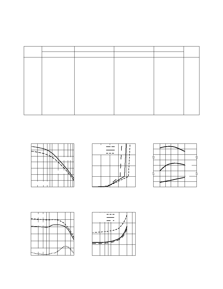
Typical Performance, T
A
= 25
∞
C
(unless otherwise noted)
G
p
(dB)
0.1
0.3 0.5
1.0
3.0
6.0
FREQUENCY (GHz)
Figure 1. Typical Power Gain vs.
Frequency, I
d
= 36 mA.
2
0
4
6
8
10
V
d
(V)
Figure 2. Device Current vs. Voltage.
0
5
10
15
20
25
30
35
0
10
20
30
40
Gain Flat to DC
I
d
(mA)
T
C
= +85
∞
C
T
C
= +25
∞
C
T
C
= ≠25
∞
C
Figure 3. Output Power at 1 dB Gain
Compression, NF and Power Gain vs.
Case Temperature, f = 1.0 GHz,
I
d
=36mA.
FREQUENCY (GHz)
Figure 4. Output Power at 1 dB Gain
Compression vs. Frequency.
FREQUENCY (GHz)
Figure 5. Noise Figure vs. Frequency.
3.0
2.5
3.5
4.0
4.5
NF (dB)
0.1
0.2 0.3
0.5
2.0
1.0
4.0
0.1
0.2 0.3
0.5
2.0
1.0
4
6
8
10
16
14
12
P
1 dB
(dBm)
I
d
= 36 mA
I
d
= 40 mA
I
d
= 20 mA
2
3
4
11
12
13
21
22
23
≠25
+25
0
+55
+85
P
1 dB
(dBm)
NF (dB)
Gp (dB)
TEMPERATURE (
∞
C)
NF
P
1 dB
G
P
I
d
= 36 mA
I
d
= 20 mA
I
d
= 20 mA
I
d
= 36 mA
I
d
= 40 mA
6-429
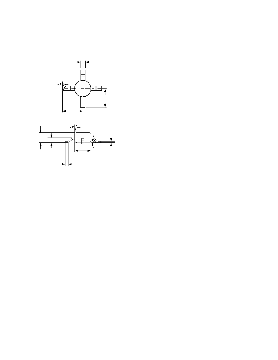
86 Plastic Package Dimensions
4
0.51
±
0.13
(0.020
±
0.005)
2.34
±
0.38
(0.092
±
0.015)
2.67
±
0.38
(0.105
±
0.15)
1
3
2
2.16
±
0.13
(0.085
±
0.005)
DIMENSIONS ARE IN MILLIMETERS (INCHES)
1.52
±
0.25
(0.060
±
0.010)
0.66
±
0.013
(0.026
±
0.005)
0.203
±
0.051
(0.006
±
0.002)
0.30 MIN
(0.012 MIN)
C
L
45
∞
5
∞
TYP.
8
∞
MAX
0
∞
MIN
GROUND
RF INPUT
RF OUTPUT
AND DC BIAS
GROUND
A08