 | –≠–ª–µ–∫—Ç—Ä–æ–Ω–Ω—ã–π –∫–æ–º–ø–æ–Ω–µ–Ω—Ç: AP134-501 | –°–∫–∞—á–∞—Ç—å:  PDF PDF  ZIP ZIP |
Alpha Industries, Inc. [781] 935-5150
∑ Fax [617] 824-4579 ∑ Email sales@alphaind.com ∑ www.alphaind.com
1
Specifications subject to change without notice. 8/01A
Tri-Band HBT Power Amplifier Module
Features
I 3.2 V Nominal Operating Voltage
I 50 Internally Matched Input and Output
I High Power Added Efficiency: 55% for
GSM and 50% for DCS and PCS
I Small Size: 10 x 8 x 1.6 mm MCM Land
Grid Array Package
I Low Current Standby Mode: < 10 µA
I Integral Band Select and Analog Power
Control
I GPRS Class 12 Capable
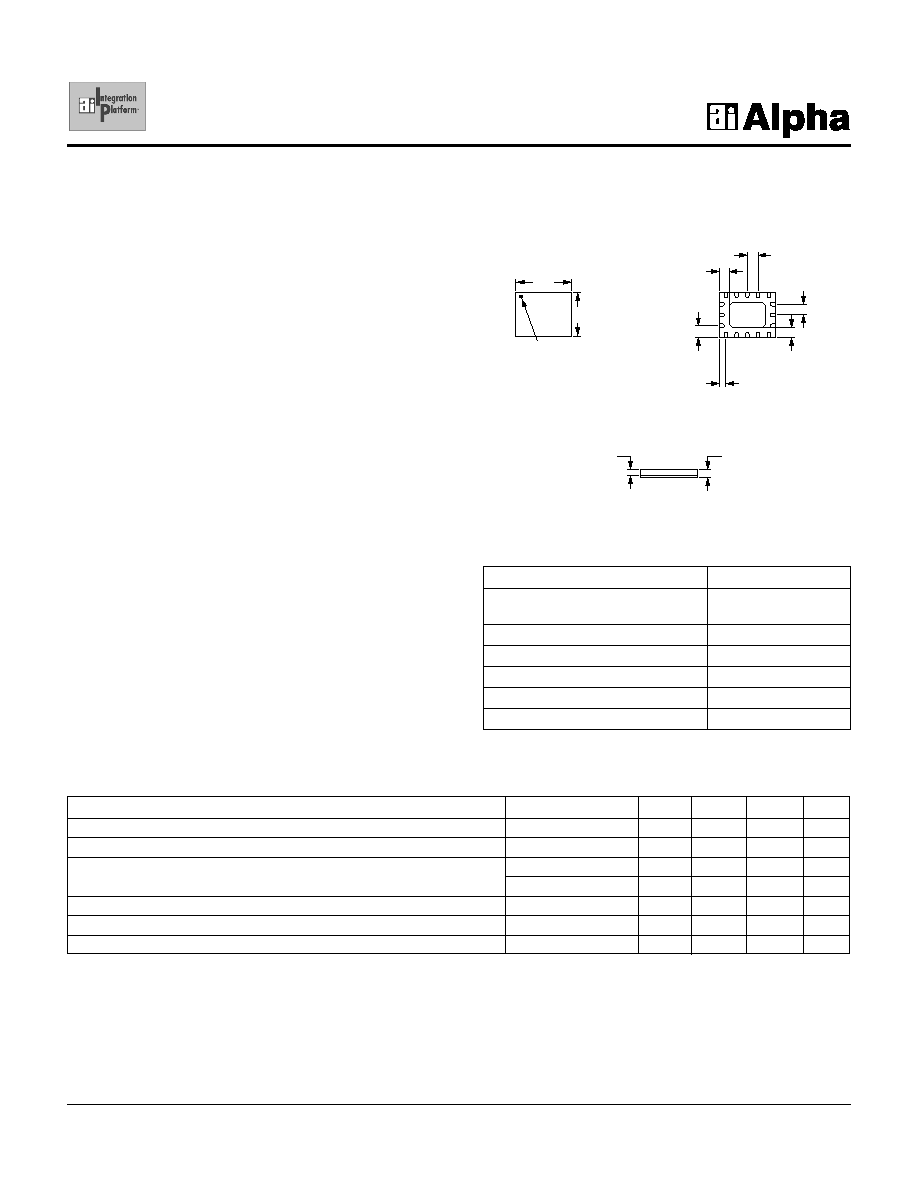
-501
AP134-501
0.394 (10.0 mm)
± 0.004 (0.1 mm)
0.315 (8.0 mm)
± 0.004 (0.1 mm)
SIDE VIEW
TOP VIEW
BOTTOM VIEW
PIN 1
INDICATOR
0.069 (1.75 mm)
± 0.002 (0.051 mm)
0.069 (1.75 mm)
± 0.002 (0.051 mm)
0.082 (2.09 mm)
± 0.002 (0.051 mm)
0.046 (1.18 mm)
± 0.002 (0.051 mm)
0.06 (1.56 mm)
± 0.004 (0.10 mm)
0.04 (1.05 mm)
± 0.002 (0.05 mm)
0.075 (1.91 mm) BSC
0.075
(1.91 mm)
BSC
MOLD CAP
16
1
Description
The AP134-501 is a high performance IC power amplifier
module designed for use as the final amplification stage
in tri-band GSM and GPRS mobile phone applications
(880≠915, 1710≠1785 and 1850≠1910 MHz). It features
3-cell battery operation, a band select switch, a single
positive analog power control input for both bands, and
exceptional power added efficiency. The amplifier is
manufactured on an advanced InGaP HBT process,
known industry-wide for its excellent reliability and
performance. The amplifier module is completely self-
contained, requiring no external matching components.
Preliminary
Parameter
Condition
Min.
Typ.
Max.
Unit
Supply Voltage
2.8
3.2
4.2
V
Leakage Current
No RF Input Power
10
µA
Band Select Voltage
GSM
0
0.5
V
DCS/PCS
2.0
2.8
V
Band Select Current
1.0
mA
Power Control Voltage
0.1
1.9
V
Power Control Current
1.0
mA
DC Specifications
Characteristic
Value
Supply Voltage V
CC
, Standby
6 V
Mode, V
APC
< 0.3, No RF Input Power
Power Control Voltage
4 V
Band Select Voltage
4 V
Input Power (CW)
15 dBm
Operating Case Temperature
-35 to +85∞C
Storage Temperature
-45 to 120∞C
Absolute Maximum Ratings
2
Alpha Industries, Inc. [781] 935-5150
∑ Fax [617] 824-4579 ∑ Email sales@alphaind.com ∑ www.alphaind.com
Specifications subject to change without notice. 8/01A
Tri-Band HBT Power Amplifier Module
AP134-501
Parameter
Condition
Min.
Typ.
Max.
Unit
Frequency
880
915
MHz
Output Power
34
35
dBm
V
CC
= 2.8 V, T = -20 to +70∞C
32.5
dBm
Dynamic Range
V
APC
= 0.1≠1.9 V
60
dB
Power Control Slope
V
APC
= 0.1≠1.9 V
75
150
dB/V
APC
Power Added Efficiency
P
OUT
= 34 dBm
50
55
%
Input Power
3
6
10
dBm
Input VSWR
P
OUT
= 5≠35 dBm
2:1
Forward Isolation
P
IN
= -5 dBm, V
APC
= 0.1 V
-40
dBm
P
IN
= 10 dBm, V
APC
= 0.1 V
-25
dBm
Harmonics
2 F
0
...7 F
0
-10
dBm
Noise in the R
X
Band
925 MHz, 100 KHz BW
-72
dBm
935 MHz, 100 KHz BW
-84
dBm
1805≠1880 MHz, 100 KHz BW
-76
dBm
1930≠1990 MHz, 100 KHz BW
-76
dBm
Ruggedness
Output VSWR = 10:1
No Module Damage
All Phase Angles, V
CC
= 4.2 V,
or Permanent
P
IN
= 10 dBm, V
APC
= 1.9 V
Performance Degradation
Stability
Output VSWR = 10:1
-36
dBm
All Phase Angles, V
CC
= 4.2 V,
P
IN
= 10 dBm, V
APC
= 1.9 V
Band to Band Isolation
2 F
0
Measured at DCS Output
-20
dBm
3 F
0
Measured at DCS Output
-20
dBm
Electrical Specifications
GSM Mode
Unless otherwise stated: pulsed operation @ 12.5% duty cycle, 50
system, V
CC
= 3.2 V, P
IN
= 6 dBm and temperature = 25∞C
Parameter
Condition
Min.
Typ.
Max.
Unit
Frequency
DCS
1710
1785
MHz
PCS
1850
1910
MHz
Output Power
31.9
32.5
dBm
V
CC
= 2.8 V, T = -20 to +70∞C
29.5
dBm
Dynamic Range
V
APC
= 0.1≠1.9 V
60
dB
Power Control Slope
V
APC
= 0.1≠1.9 V
75
150
dB/V
APC
Power Added Efficiency
P
OUT
= 31.9 dBm
42
50
%
Input Power
3
6
10
dBm
Input VSWR
P
OUT
= 0≠32 dBm
2:1
Forward Isolation
P
IN
= -5 dBm, V
APC
= 0.1 V
-48
dBm
P
IN
= 10 dBm, V
APC
= 0.1 V
-20
dBm
Harmonics
2 F
0
...7 F
0
-10
dBm
Noise in the R
X
Band
1805≠1880 MHz, 100 KHz BW
-76
dBm
Ruggedness
Output VSWR = 10:1
No Module Damage
All Phase Angles, V
CC
= 4.2 V,
or Permanent
P
IN
=10 dBm, V
APC
= 1.9 V
Performance Degradation
Stability
Output VSWR = 10:1
-36
dBm
All Phase Angles, V
CC
= 4.2 V,
P
IN
= 10 dBm, V
APC
= 1.9 V
DCS/PCS Mode
Unless otherwise stated: pulsed operation @ 12.5% duty cycle, 50
system, V
CC
= 3.2 V, P
IN
= 6 dBm and temperature = 25∞C
Alpha Industries, Inc. [781] 935-5150
∑ Fax [617] 824-4579 ∑ Email sales@alphaind.com ∑ www.alphaind.com
3
Specifications subject to change without notice. 8/01A
Tri-Band HBT Power Amplifier Module
AP134-501
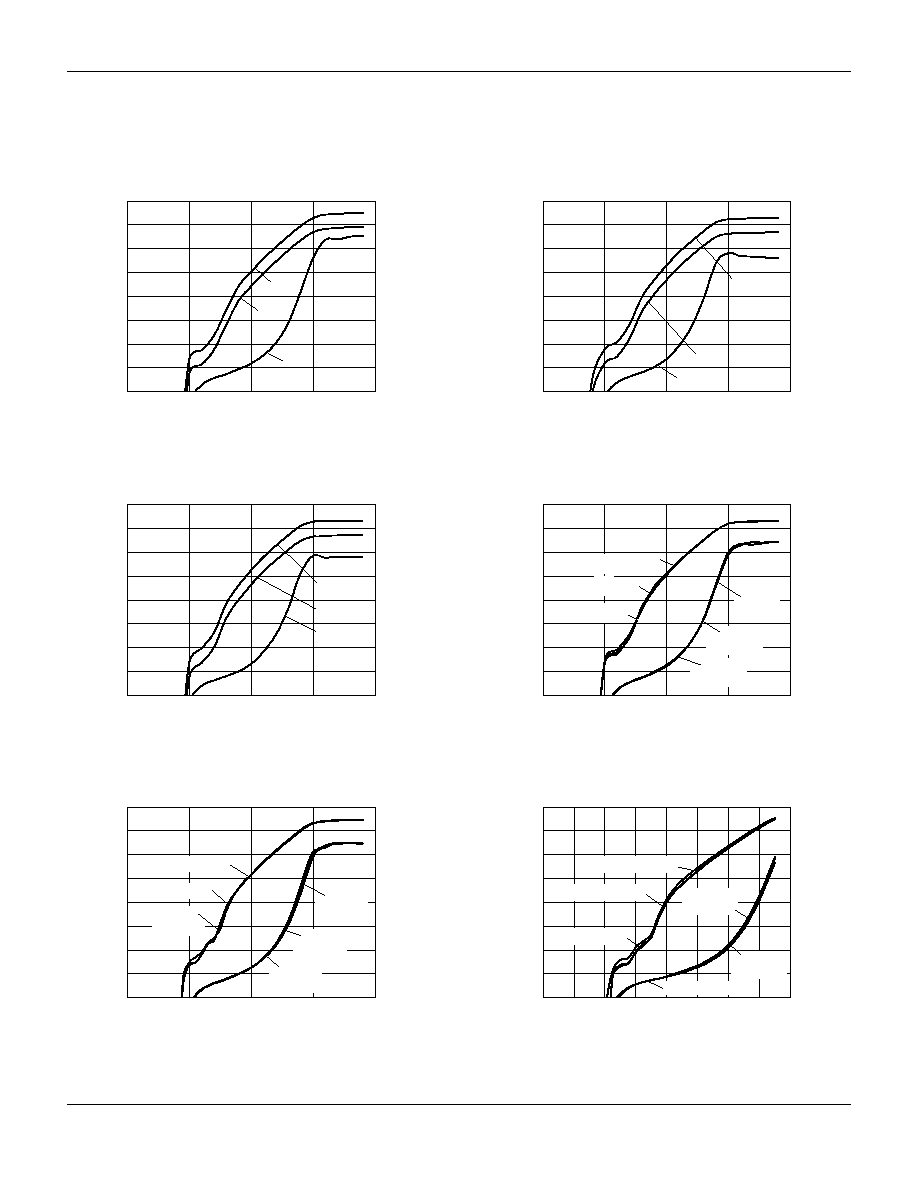
P
OUT
(dBm) and Gain (dB)
Power Added Efficiency (%)
V
APC
(V)
V
CC
= 3.2 V, Frequency = 900 MHz,
P
IN
= 6 dBm
-40
-30
-20
-10
0
10
20
30
40
0
0.5
1.0
1.5
2.0
-10
0
10
20
30
40
50
60
70
P
OUT
Gain
PAE
P
OUT
(dBm) and Gain (dB)
Power Added Efficiency (%)
V
APC
(V)
V
CC
= 3.2 V, Frequency = 1750 MHz,
P
IN
= 6 dBm
-40
-30
-20
-10
0
10
20
30
40
0
0.5
1.0
1.5
2.0
-10
0
10
20
30
40
50
60
70
P
OUT
Gain
PAE
P
OUT
(dBm) and Gain (dB)
Power Added Efficiency (%)
V
APC
(V)
V
CC
= 3.2 V, Frequency = 1910 MHz,
P
IN
= 6 dBm
-40
-30
-20
-10
0
10
20
30
40
0
0.5
1.0
1.5
2.0
-10
0
10
20
30
40
50
60
70
P
OUT
Gain
PAE
P
OUT
(dBm) and Gain (dB)
Power Added Efficiency (%)
V
APC
(V)
V
CC
= 2.8 V, Frequency = 900 MHz,
P
IN
= 6 dBm
-40
-30
-20
-10
0
10
20
30
40
0
0.5
1.0
1.5
2.0
-10
0
10
20
30
40
50
60
70
P
OUT
880 MHz
P
OUT
900 MHz
P
OUT
915 MHz
PAE
880 MHz
PAE
900 MHz
PAE
915 MHz
P
OUT
(dBm)
Power Added Efficiency (%)
V
APC
(V)
-40
-30
-20
-10
0
10
20
30
40
0
0.5
1.0
1.5
2.0
-10
0
10
20
30
40
50
60
70
P
OUT
and PAE vs. V
APC
and
Frequency, V
CC
= 3.2 V, P
IN
= 6 dBm
P
OUT
880 MHz
P
OUT
900 MHz
P
OUT
915 MHz
PAE
880 MHz
PAE
900 MHz
PAE
915 MHz
P
OUT
(dBm)
Power Added Efficiency (%)
V
APC
(V)
P
OUT
and PAE vs. V
APC
and Frequency, V
CC
= 4.2 V, P
IN
= 6 dBm
-40
-30
-20
-10
0
10
20
30
40
-10
0
10
20
30
40
50
60
70
0
0.2
0.4
0.6
0.8
1.0
1.2
1.4
1.6
P
OUT
880 MHz
P
OUT
900 MHz
P
OUT
915 MHz
PAE
880 MHz
PAE
900 MHz
PAE 915 MHz
Typical Performance Data
All data taken under CW conditions and include 0.2 dB of input and output fixture losses deembedded, GSM class 4 pulsed
performance adds 0.5 dB of output power and 5≠7% in PAE.
4
Alpha Industries, Inc. [781] 935-5150
∑ Fax [617] 824-4579 ∑ Email sales@alphaind.com ∑ www.alphaind.com
Specifications subject to change without notice. 8/01A
Tri-Band HBT Power Amplifier Module
AP134-501
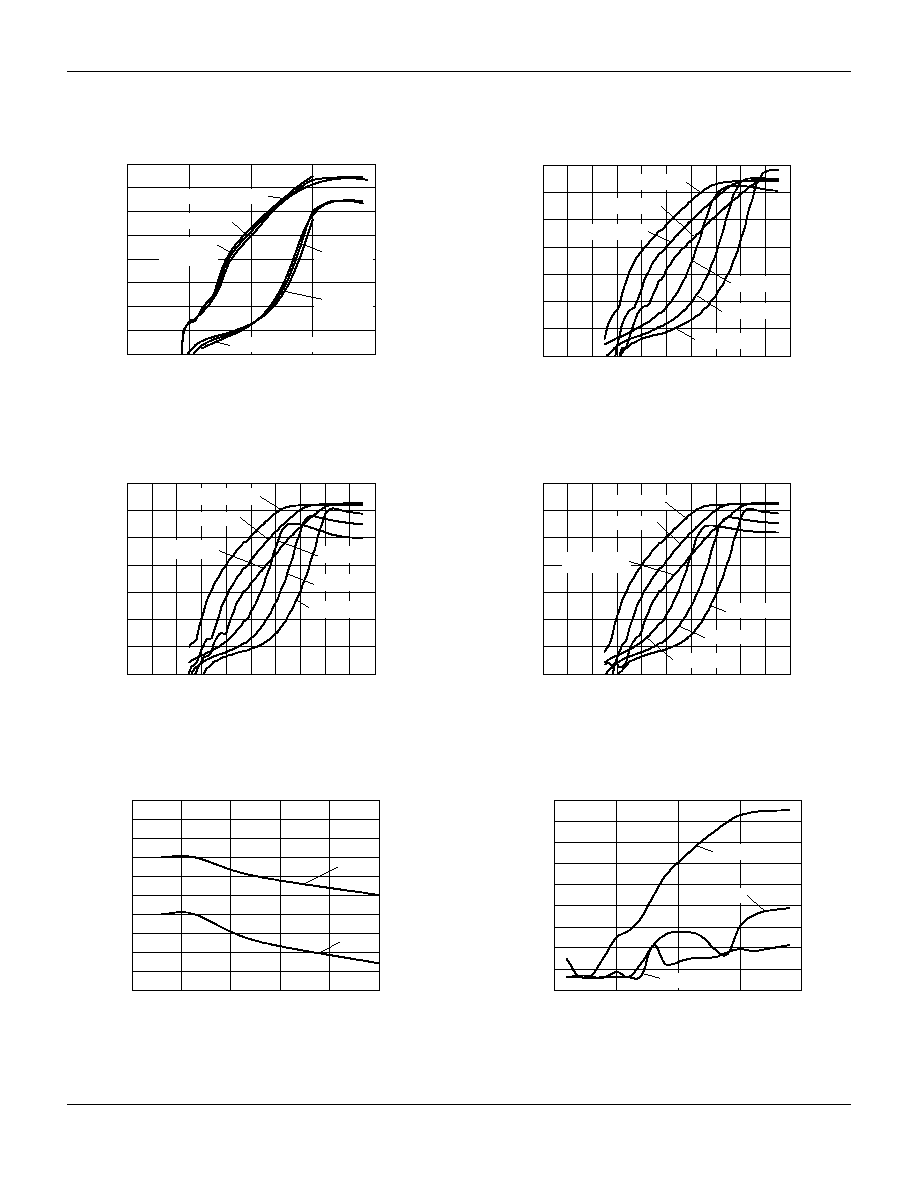
P
OUT
(dBm)
Power Added Efficiency (%)
V
APC
(V)
-40
-30
-20
-10
0
10
20
30
40
0
0.5
1.0
1.5
2.0
-10
0
10
20
30
40
50
60
70
P
OUT
and PAE vs. V
CC
and V
APC
P
IN
= 6 dBm
P
OUT
@
V
CC
= 2.8
P
OUT
@ V
CC
= 3.2
P
OUT
@ V
CC
= 4.2
PAE @ V
CC
= 2.8
PAE @
V
CC
= 3.2
PAE @
V
CC
= 4.2
0.2
0
0.4 0.6 0.8 1.0 1.2 1.4 1.6 1.8 2.0
P
OUT
(dBm)
Power Added Efficiency (%)
Control Voltage ≠ V
APC
(V)
-30
-20
-10
0
10
20
30
40
-10
0
10
20
30
40
50
60
P
OUT
and PAE vs. Temperature
V
CC
= 3.2 V, P
IN
= 6 dBm,
Frequency = 880 MHz
P
OUT
-25∞C
P
OUT
25∞C
P
OUT
75∞C
PAE -25∞C
PAE 25∞C
PAE 75∞C
0.2
0
0.4 0.6 0.8 1.0 1.2 1.4 1.6 1.8 2.0
P
OUT
(dBm)
Power Added Efficiency (%)
Control Voltage ≠ V
APC
(V)
-30
-20
-10
0
10
20
30
40
-10
0
10
20
30
40
50
60
P
OUT
and PAE vs. Temperature
V
CC
= 3.2 V, P
IN
= 6 dBm,
Frequency = 1710 MHz
P
OUT
-25∞C
P
OUT
25∞C
P
OUT
75∞C
PAE -25∞C
PAE 25∞C
PAE 75∞C
0.2
0
0.4 0.6 0.8 1.0 1.2 1.4 1.6 1.8 2.0
P
OUT
(dBm)
Power Added Efficiency (%)
Control Voltage ≠ V
APC
(V)
-30
-20
-10
0
10
20
30
40
-10
0
10
20
30
40
50
60
P
OUT
and PAE vs. Temperature
V
CC
= 3.2 V, P
IN
= 6 dBm,
Frequency = 1850 MHz
P
OUT
-25∞C
P
OUT
25∞C
P
OUT
75∞C
PAE -25∞C
PAE 25∞C
PAE 75∞C
P
OUT
(dBm)
Power Added Efficiency (%)
Duty Cycle (%)
Duty Cycle Effects on Module Performance
V
CC
= 3.2 V, Frequency = 900 MHz,
P
IN
= 6 dBm
34.0
34.2
34.4
34.6
34.8
35.0
35.2
35.4
35.6
35.8
36.0
0
20
40
60
80
100
50
51
52
53
54
55
56
57
58
59
60
P
OUT
PAE
P
OUT
, F
0
2 F
0
and 3 F
0
(dBm)
-50
-40
-30
-20
-10
0
10
20
30
40
0
0.5
1.0
1.5
2.0
Harmonic Performance V
CC
= 3.2 V,
Frequency = 900 MHz, P
IN
= 6 dBm
V
APC
(V)
F
0
(dBm)
2 F
0
(dBm)
3 F
0
(dBm)
All data taken under CW conditions and include 0.2 dB of input and output fixture losses deembedded, GSM class 4 pulsed
performance adds 0.5 dB of output power and 5≠7% in PAE.
Alpha Industries, Inc. [781] 935-5150
∑ Fax [617] 824-4579 ∑ Email sales@alphaind.com ∑ www.alphaind.com
5
Specifications subject to change without notice. 8/01A
Tri-Band HBT Power Amplifier Module
AP134-501
1
2
3
4
5
13
12
11
10
9
6
7
8
16
15
14
CMOS ASIC
V
APC
GND
V
CC
V
CC
V
BS
GND
DCS/PCS In
GSM In
V
cc
V
CC
GND
GND
GND
GND
DCS/PCS Out
GSM Out
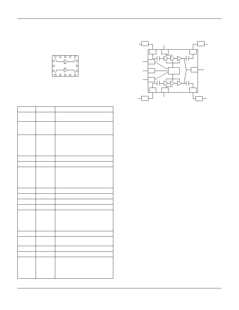
Pin Out
1
16
2
3
4
5
6
13
9
11
V
CC
DCS/
PCS In
GSM
In
GSM
Out
V
APC
V
CC
V
CC
DCS/
PCS Out
V
CC
V
BS
50
Microstrip
50
Microstrip
50
Microstrip
50
Microstrip
Application Schematic
Pin Out Description
Pin
Symbol
Description
1
DCS/
RF input to DCS/PCS power amplifier.
PCS_In
2
V
APC
Analog power control input voltage.
10 nF RF bypassing capacitor
recommended.
3
V
CC
Power supply input voltage. A 10
µF
RF bypassing capacitor is required.
This capacitor is only required to help
reduce power supply ripple on the test
board.
4
V
BS
Band select input voltage.
5
GSM_In
RF input to GSM power amplifier.
6
VCC
Power supply input voltage. 10
µF
RF bypassing capacitor is required.
This capacitor is only required to help
reduce power supply ripple on the test
board.
7
GND
Ground connection.
8
GND
Ground connection.
9
GSM_Out
RF output for GSM amplifier.
10
GND
Ground connection.
11
V
CC
Power supply input voltage. 10
µF
RF bypassing capacitor is required.
This capacitor is only required to help
reduce power supply ripple on the test
board.
12
GND
Ground connection.
13
DCS/
RF output for DCS/PCS power
PCS_Out
amplifier.
14
GND
Ground connection.
15
GND
Ground connection.
16
V
CC
Power supply input voltage. 10
µF
RF bypassing capacitor is required.
This capacitor is only required to help
reduce power supply ripple on the test
board.