Äîêóìåíòàöèÿ è îïèñàíèÿ www.docs.chipfind.ru

Publication Number 23695 Revision
C
Amendment +1 Issue
Date
October 7, 2004
July 2003
The following document specifies Spansion memory products that are now offered by both Advanced
Micro Devices and Fujitsu. Although the document is marked with the name of the company that
originally developed the specification, these products will be offered to customers of both AMD and
Fujitsu.
Continuity of Specifications
There is no change to this datasheet as a result of offering the device as a Spansion product. Any
changes that have been made are the result of normal datasheet improvement and are noted in the
document revision summary, where supported. Future routine revisions will occur when appropri-
ate, and changes will be noted in a revision summary.
Continuity of Ordering Part Numbers
AMD and Fujitsu continue to support existing part numbers beginning with "Am" and "MBM". To
order these products, please use only the Ordering Part Numbers listed in this document.
For More Information
Please contact your local AMD or Fujitsu sales office for additional information about Spansion mem-
ory solutions.
Am29DL640D
Data Sheet
For new designs involving TSOP packages, S29JL064H supersedes Am29DL640D and is the factory-recom-
mended migration path. Please refer to the S29JL064H datasheet for specifications and ordering information.
For new designs involving Fine-pitch BGA (FBGA) packages, S29PL064J supersedes Am29DL640D and is the
factory-recommended migration path. Please refer to the S29PL064J Datasheet for specifications and ordering
information.

Publication# 23695
Rev: C Amendment/1
Issue Date: October 7, 2004
Refer to AMD's Website (www.amd.com) for the latest information.
Am29DL640D
64 Megabit (8 M x 8-Bit/4 M x 16-Bit)
CMOS 3.0 Volt-only, Simultaneous Read/Write Flash Memory
DISTINCTIVE CHARACTERISTICS
ARCHITECTURAL ADVANTAGES
Simultaneous Read/Write operations
-- Data can be continuously read from one bank while
executing erase/program functions in another bank.
-- Zero latency between read and write operations
Flexible Bank
TM
architecture
-- Read may occur in any of the three banks not being
written or erased.
-- Four banks may be grouped by customer to achieve
desired bank divisions.
Boot Sectors
-- Top and bottom boot sectors in the same device
-- Any combination of sectors can be erased
Manufactured on 0.23 µm process technology
SecSiTM (Secured Silicon) Sector: Extra 256 Byte
sector
--
Factory locked and identifiable:
16 bytes available for
secure, random factory Electronic Serial Number;
verifiable as factory locked through autoselect
function. ExpressFlash option allows entire sector to
be available for factory-secured data
--
Customer lockable:
Can be read or programmed just
like other sectors. Once locked, data cannot be
changed
Zero Power Operation
-- Sophisticated power management circuits reduce
power consumed during inactive periods to nearly
zero.
Compatible with JEDEC standards
-- Pinout and software compatible with
single-power-supply flash standard
PACKAGE OPTIONS
63-ball Fine Pitch BGA
48-pin TSOP
PERFORMANCE CHARACTERISTICS
High performance
-- Access time as fast as 90 ns
-- Program time: 4 µs/word typical utilizing Accelerate
function
Ultra low power consumption (typical values)
-- 2 mA active read current at 1 MHz
-- 10 mA active read current at 5 MHz
-- 200 nA in standby or automatic sleep mode
Minimum 1 million erase cycles guaranteed per
sector
20 year data retention at 125°C
-- Reliable operation for the life of the system
SOFTWARE FEATURES
Data Management Software (DMS)
-- AMD-supplied software manages data programming,
enabling EEPROM emulation
-- Eases historical sector erase flash limitations
Supports Common Flash Memory Interface (CFI)
Program/Erase Suspend/Erase Resume
-- Suspends program/erase operations to allow
programming/erasing in same bank
Data# Polling and Toggle Bits
-- Provides a software method of detecting the status of
program or erase cycles
Unlock Bypass Program command
-- Reduces overall programming time when issuing
multiple program command sequences
HARDWARE FEATURES
Ready/Busy# output (RY/BY#)
-- Hardware method for detecting program or erase
cycle completion
Hardware reset pin (RESET#)
-- Hardware method of resetting the internal state
machine to the read mode
WP#/ACC input pin
-- Write protect (WP#) function protects sectors 0, 1,
140, and 141, regardless of sector protect status
-- Acceleration (ACC) function accelerates program
timing
Sector protection
-- Hardware method of locking a sector, either
in-system or using programming equipment, to
prevent any program or erase operation within that
sector
-- Temporary Sector Unprotect allows changing data in
protected sectors in-system
For new designs involving TSOP packages, S29JL064H supersedes Am29DL640D and is the factory-recommended migration path. Please refer to the S29JL064H datasheet for specifica-
tions and ordering information. For new designs involving Fine-pitch BGA (FBGA) packages, S29PL064J supersedes Am29DL640D and is the factory-recommended migration path. Please
refer to the S29PL064J Datasheet for specifications and ordering information.
2
Am29DL640D
October 7, 2004
GENERAL DESCRIPTION
The Am29DL640D is a 64 megabit, 3.0 volt-only flash
memory device, organized as 4,194,304 words of 16
bits each or 8,388,608 bytes of 8 bits each. Word
mode data appears on DQ0DQ15; byte mode data
appears on DQ0DQ7. The device is designed to be
programmed in-system with the standard 3.0 volt V
CC
supply, and can also be programmed in standard
EPROM programmers.
The device is available with an access time of 90 or
120 ns and is offered in 48-pin TSOP and 63-ball
Fine-Pitch BGA. Standard control pins--chip enable
( C E # ), w r i te e n able ( W E # ), a nd ou tp u t en a bl e
(OE#)--control normal read and write operations, and
avoid bus contention issues.
The device requires only a single 3.0 volt power sup-
ply for both read and write functions. Internally
generated and regulated voltages are provided for the
program and erase operations.
Simultaneous Read/Write Operations with
Zero Latency
The Simultaneous Read/Write architecture provides
simultaneous operation by dividing the memory
space into four banks, two 8 Mb banks with small and
large sectors, and two 24 Mb banks of large sectors.
Sector addresses are fixed, system software can be
used to form user-defined bank groups.
During an Erase/Program operation, any of the three
non-busy banks may be read from. Note that only two
banks can operate simultaneously. The device can im-
prove overall system performance by allowing a host
sy ste m t o p ro gra m o r e ra se i n o ne ba n k, th e n
immediately and simultaneously read from the other
bank, with zero latency. This releases the system from
waiting fo r the completion o f progra m or erase
operations.
The Am29DL640D can be organized as both a top and
bottom boot sector configuration.
Am29DL640D Features
The SecSiTM (Secured Silicon) Sector is an extra
256 byte sector capable of being permanently locked
by AMD or customers. The SecSi Indicator Bit (DQ7)
is permanently set to a 1 if the part is factory locked,
and set to a 0 if customer lockable. This way, cus-
tomer lockable parts can never be used to replace a
factory locked part.
Factory locked parts provide several options. The
SecSi Sector may store a secure, random 16 byte
ESN (Electronic Serial Number), customer code (pro-
grammed through AMD's ExpressFlash service), or
both. Customer Lockable parts may utilize the SecSi
Sector as bonus space, reading and writing like any
other flash sector, or may permanently lock their own
code there.
DMS (Data Management Software) allows systems
to easily take advantage of the advanced architecture
of the simultaneous read/write product line by allowing
removal of EEPROM devices. DMS will also allow the
system software to be simplified, as it will perform all
functions necessary to modify data in file structures,
as opposed to single-byte modifications. To write or
update a particular piece of data (a phone number or
configuration data, for example), the user only needs
to state which piece of data is to be updated, and
where the updated data is located in the system. This
i s a n a d va n t a g e c o m p a r e d t o s y s t e m s w h e r e
user-written software must keep track of the old data
location, status, logical to physical translation of the
data onto the Flash memory device (or memory de-
vices), and more. Using DMS, user-written software
does not need to interface with the Flash memory di-
rectly. Instead, the user's software accesses the Flash
memory by calling one of only six functions. AMD pro-
vides this software to simplify system design and
software integration efforts.
The device offers complete compatibility with the
JEDEC single-power-supply Flash command set
standard. Commands are written to the command
register using standard microprocessor write timings.
Reading data out of the device is similar to reading
from other Flash or EPROM devices.
The host system can detect whether a program or
erase operation is complete by using the device sta-
tus bits: RY/BY# pin, DQ7 (Data# Polling) and
DQ6/DQ2 (toggle bits). After a program or erase cycle
has been completed, the device automatically returns
to the read mode.
The sector erase architecture allows memory sec-
tors to be erased and reprogrammed without affecting
the data contents of other sectors. The device is fully
erased when shipped from the factory.
Hardware data protection measures include a low
V
CC
detector that automatically inhibits write opera-
tions during power transitions. The hardware sector
protection feature disables both program and erase
operations in any combination of the sectors of mem-
o r y. T h i s c a n b e a c h i e v e d i n - s y s t e m o r v i a
programming equipment.
The device offers two power-saving features. When
addresses have been stable for a specified amount of
time, the device enters the automatic sleep mode.
Th e syste m can also place the device into th e
standby mode. Power consumption is greatly re-
duced in both modes.
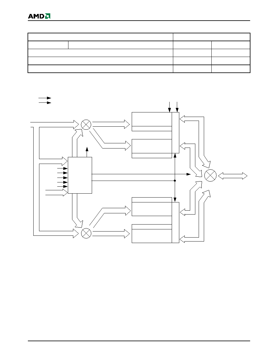
Bank
Megabits
Sector Sizes
Bank 1
8 Mb
Eight 8 Kbyte/4 Kword,
Fifteen 64 Kbyte/32 Kword
Bank 2
24 Mb
Forty-eight 64 Kbyte/32 Kword
Bank 3
24 Mb
Forty-eight 64 Kbyte/32 Kword
Bank 4
8 Mb
Eight 8 Kbyte/4 Kword,
Fifteen 64 Kbyte/32 Kword

October 7, 2004
Am29DL640D
3
TABLE OF CONTENTS
Product Selector Guide . . . . . . . . . . . . . . . . . . . . . 5
Block Diagram . . . . . . . . . . . . . . . . . . . . . . . . . . . . 5
Connection Diagrams . . . . . . . . . . . . . . . . . . . . . . . 6
Pin Description . . . . . . . . . . . . . . . . . . . . . . . . . . . . 7
Ordering Information . . . . . . . . . . . . . . . . . . . . . . . 8
Device Bus Operations . . . . . . . . . . . . . . . . . . . . . . 9
Table 1. Am29DL640D Device Bus Operations ................................9
Requirements for Reading Array Data ..................................... 9
Writing Commands/Command Sequences ............................ 10
Accelerated Program Operation ............................................. 10
Autoselect Functions .............................................................. 10
Simultaneous Read/Write Operations with Zero Latency ....... 10
Automatic Sleep Mode ........................................................... 11
RESET#: Hardware Reset Pin ............................................... 11
Output Disable Mode .............................................................. 11
Table 2. Am29DL640D Sector Architecture ....................................11
Table 3. Bank Address ....................................................................14
Table 5. Am29DL640D Autoselect Codes, (High Voltage Method) 15
Table 6. Am29DL640D Boot Sector/Sector Block Addresses for Pro-
tection/Unprotection ........................................................................16
Write Protect (WP#) ................................................................ 17
Table 7. WP#/ACC Modes ..............................................................17
Temporary Sector Unprotect .................................................. 17
Figure 1. Temporary Sector Unprotect Operation........................... 17
Figure 2. In-System Sector Protect/Unprotect Algorithms .............. 18
SecSiTM (Secured Silicon) Sector
Flash Memory Region ............................................................ 19
Figure 3. SecSi Sector Protect Verify.............................................. 20
Hardware Data Protection ...................................................... 20
Low VCC Write Inhibit ............................................................ 20
Write Pulse "Glitch" Protection ............................................... 20
Logical Inhibit .......................................................................... 20
Power-Up Write Inhibit ............................................................ 20
Common Flash Memory Interface (CFI) . . . . . . . 20
Command Definitions . . . . . . . . . . . . . . . . . . . . . . 24
Reading Array Data ................................................................ 24
Reset Command ..................................................................... 24
Autoselect Command Sequence ............................................ 24
Enter SecSiTM Sector/Exit SecSi Sector
Command Sequence .............................................................. 24
Byte/Word Program Command Sequence ............................. 25
Unlock Bypass Command Sequence ..................................... 25
Figure 4. Program Operation .......................................................... 26
Chip Erase Command Sequence ........................................... 26
Sector Erase Command Sequence ........................................ 26
Erase Suspend/Erase Resume Commands ........................... 27
Figure 5. Erase Operation............................................................... 27
Write Operation Status . . . . . . . . . . . . . . . . . . . . . 29
DQ7: Data# Polling ................................................................. 29
Figure 6. Data# Polling Algorithm ................................................... 29
DQ6: Toggle Bit I .................................................................... 30
Figure 7. Toggle Bit Algorithm......................................................... 30
DQ2: Toggle Bit II ................................................................... 31
Reading Toggle Bits DQ6/DQ2 .............................................. 31
DQ5: Exceeded Timing Limits ................................................ 31
DQ3: Sector Erase Timer ....................................................... 31
Table 13. Write Operation Status ................................................... 32
Absolute Maximum Ratings . . . . . . . . . . . . . . . . 33
Figure 8. Maximum Negative Overshoot Waveform ...................... 33
Figure 9. Maximum Positive Overshoot Waveform........................ 33
DC Characteristics . . . . . . . . . . . . . . . . . . . . . . . . 34
Figure 10. I
CC1
Current vs. Time (Showing Active and
Automatic Sleep Currents) ............................................................. 35
Figure 11. Typical I
CC1
vs. Frequency ............................................ 35
Test Conditions . . . . . . . . . . . . . . . . . . . . . . . . . . 36
Figure 12. Test Setup.................................................................... 36
Figure 13. Input Waveforms and Measurement Levels ................. 36
AC Characteristics . . . . . . . . . . . . . . . . . . . . . . . . 37
Read-Only Operations ........................................................... 37
Figure 14. Read Operation Timings ............................................... 37
Hardware Reset (RESET#) .................................................... 38
Figure 15. Reset Timings ............................................................... 38
Word/Byte Configuration (BYTE#) .......................................... 39
Figure 16. BYTE# Timings for Read Operations............................ 39
Figure 17. BYTE# Timings for Write Operations............................ 39
Erase and Program Operations .............................................. 40
Figure 18. Program Operation Timings.......................................... 41
Figure 19. Accelerated Program Timing Diagram .......................... 41
Figure 20. Chip/Sector Erase Operation Timings .......................... 42
Figure 21. Back-to-back Read/Write Cycle Timings ...................... 43
Figure 22. Data# Polling Timings (During Embedded Algorithms). 43
Figure 23. Toggle Bit Timings (During Embedded Algorithms)...... 44
Figure 24. DQ2 vs. DQ6................................................................. 44
Temporary Sector Unprotect .................................................. 45
Figure 25. Temporary Sector Unprotect Timing Diagram .............. 45
Figure 26. Sector/Sector Block Protect and
Unprotect Timing Diagram ............................................................. 46
Alternate CE# Controlled Erase and Program Operations ..... 47
Figure 27. Alternate CE# Controlled Write (Erase/Program)
Operation Timings.......................................................................... 48
Erase And Programming Performance . . . . . . . 49
Latchup Characteristics . . . . . . . . . . . . . . . . . . . . 49
TSOP Pin Capacitance . . . . . . . . . . . . . . . . . . . . . 49
Data Retention. . . . . . . . . . . . . . . . . . . . . . . . . . . . 49
Physical Dimensions . . . . . . . . . . . . . . . . . . . . . . 50
FBE063--63-Ball Fine-Pitch Ball Grid Array (FBGA)
12 x 11 mm package .............................................................. 50
TS 048--48-Pin Standard TSOP ............................................ 51
Revision Summary . . . . . . . . . . . . . . . . . . . . . . . . 52
Revision A (March 5, 2001) .................................................... 52
Revision A+1 (March 9, 2001) ................................................ 52
Revision B (August 10, 2001) ................................................. 52
Revision B+1 (August 30, 2001) ............................................. 52
Revision B+2 (October 11, 2001) ........................................... 52
Revision B+3 (November 5, 2001) ......................................... 52
Revision B+4 (April 15, 2002) ................................................. 52
Revision B+5 (August 19, 2002) ............................................. 52
Revision C (January 10, 2003) ............................................... 53
Revision C+1 (September 15, 2004) ...................................... 53
4
Am29DL640D
October 7, 2004
PRODUCT SELECTOR GUIDE
BLOCK DIAGRAM
Part Number
Am29DL640D
Speed Option
Standard Voltage Range: V
CC
= 2.73.6 V
90
120
Max Access Time (ns), t
ACC
90
120
CE# Access (ns), t
CE
90
120
OE# Access (ns), t
OE
35
50
V
CC
V
SS
Bank 1 Address
Bank 2 Address
A21A0
RESET#
WE#
CE#
BYTE#
DQ0DQ15
WP#/ACC
STATE
CONTROL
&
COMMAND
REGISTER
RY/BY#
Bank 1
X-Decoder
OE#
BYTE#
DQ15DQ0
Status
Control
A21A0
A21A0
A21A0
A21A0
DQ15DQ0
DQ15DQ0
DQ15DQ0
DQ15DQ0
Mux
Mux
Mux
Bank 2
X-Decoder
Y-gate
Bank 3
X-Decoder
Bank 4
X-Decoder
Y-gate
Bank 3 Address
Bank 4 Address
Document Outline
- Am29DL640D
- Am29DL640D
- Distinctive Characteristics
- General Description
- Product Selector Guide
- Block Diagram
- Connection Diagrams
- Pin Description
- Logic Symbol
- Ordering Information
- Device Bus Operations
- Common Flash Memory Interface (CFI)
- Command Definitions
- Write Operation Status
- Absolute Maximum Ratings
- DC Characteristics
- Test Conditions
- AC Characteristics
- Erase And Programming Performance
- Latchup Characteristics
- TSOP Pin Capacitance
- Data Retention
- Physical Dimensions
- Revision Summary
- Revision A (March 5, 2001)
- Revision A+1 (March 9, 2001)
- Revision B (August 10, 2001)
- Revision B+1 (August 30, 2001)
- Revision B+2 (October 11, 2001)
- Revision B+3 (November 5, 2001)
- Revision B+4 (April 15, 2002)
- Revision B+5 (August 19, 2002)
- Revision C (January 10, 2003)
- Revision C+1 (October 7, 2004)