This Data Sheet states AMD's current technical specifications regarding the Products described herein. This Data
Sheet may be revised by subsequent versions or modifications due to changes in technical specifications.
Publication# 22140
Rev: D Amendment/+1
Issue Date: November 13, 2000
Am29LV010B
1 Megabit (128 K x 8-Bit)
CMOS 3.0 Volt-only Uniform Sector Flash Memory
DISTINCTIVE CHARACTERISTICS
s
Single power supply operation
-- Full voltage range: 2.7 to 3.6 volt read and write
operations for battery-powered applications
-- Regulated voltage range: 3.0 to 3.6 volt read and
write operations and for compatibility with high
performance 3.3 volt microprocessors
s
Manufactured on 0.32 µm process technology
s
High performance
-- Full voltage range: access times as fast as 55 ns
-- Regulated voltage range: access times as fast as
45 ns
s
Ultra low power consumption (typical values at
5 MHz)
-- 200 nA Automatic Sleep mode current
-- 200 nA standby mode current
-- 7 mA read current
-- 15 mA program/erase current
s
Flexible sector architecture
-- Eight 16 Kbyte
-- Supports full chip erase
-- Sector Protection features:
Hardware method of locking a sector to prevent
any program or erase operations within that sector
Sectors can be locked in-system or via
programming equipment
Temporary Sector Unprotect feature allows code
changes in previously locked sectors
s
Unlock Bypass Mode Program Command
-- Reduces overall programming time when issuing
multiple program command sequences
s
Embedded Algorithms
-- Embedded Erase algorithm automatically
preprograms and erases the entire chip or any
combination of designated sectors
-- Embedded Program algorithm automatically
writes and verifies data at specified addresses
s
Minimum 1,000,000 write cycle guarantee per
sector
s
20 Year data retention at 125
∞
C
-- Reliable operation for the life of the system
s
Package option
-- 32-pin TSOP
-- 32-pin PLCC
s
Compatibility with JEDEC standards
-- Pinout and software compatible with single-
power supply Flash
-- Superior inadvertent write protection
s
Data# Polling and toggle bits
-- Provides a software method of detecting program
or erase operation completion
s
Erase Suspend/Erase Resume
-- Supports reading data from or programming data
to a sector that is not being erased

2
Am29LV010B
GENERAL DESCRIPTION
The Am29LV010B is a 1 Mbit, 3.0 Volt-only Flash
memory device organized as 131,072 bytes. The
Am29LV010B has a uniform sector architecture.
The device is offered in 32-pin PLCC and 32-pin TSOP
packages. The byte-wide (x8) data appears on DQ7-DQ0.
All read, erase, and program operations are accomplished
using only a single power supply. The device can also be
programmed in standard EPROM programmers.
The standard Am29LV010B offers access times of 45,
55, 70, and 90 ns (100 ns part is also available),
allowing high speed microprocessors to operate
without wait states. To eliminate bus contention, the
device has separate chip enable (CE#), write enable
(WE#) and output enable (OE#) controls.
The device requires only a single power supply
(2.7V-3.6V) for both read and write functions. Internally
generated and regulated voltages are provided for the
program and erase operations.
The device is entirely command set compatible with the
JEDEC single-power-supply Flash standard. Com-
mands are written to the command register using
standard microprocessor write timings. Register con-
tents serve as input to an internal state-machine that
controls the erase and programming circuitry. Write
cycles also internally latch addresses and data needed
for the programming and erase operations. Reading
data out of the device is similar to reading from other
Flash or EPROM devices.
Device programming occurs by executing the program
command sequence. This initiates the Embedded
Program algorithm--an internal algorithm that auto-
matically times the program pulse widths and verifies
proper cell margin. The Unlock Bypass mode facili-
tates faster programming times by requiring only two
write cycles to program data instead of four.
Device erasure o ccu rs by executin g th e era se
command sequence. This initiates the Embedded
Erase algorithm--an internal algorithm that automati-
cally preprograms the array (if it is not already
programmed) before executing the erase operation.
During erase, the device automatically times the erase
pulse widths and verifies proper cell margin.
The host system can detect whether a program or
erase operation is complete by reading the DQ7 (Data#
Polling) and DQ6 (toggle) status bits. After a program
or erase cycle has been completed, the device is ready
to read array data or accept another command.
The sector erase architecture allows memory sectors
to be erased and reprogrammed without affecting the
data contents of other sectors. The device is fully
erased when shipped from the factory.
Hardware data protection measures include a low
V
CC
detector that automatically inhibits write opera-
tions during power transitions. The hardware sector
protection feature disables both program and erase
operations in any combination of the sectors of
memory. This can be achieved in-system or via pro-
gramming equipment.
The Erase Suspend feature enables the user to put
erase on hold for any period of time to read data from,
or program data to, any sector that is not selected for
erasure. True background erase can thus be achieved.
The device offers two power-saving features. When
addresses have been stable for a specified amount of
time, the device enters the automatic sleep mode.
The system can also place the device into the standby
mode. Power consumption is greatly reduced in both
these modes.
AMD's Flash technology combines years of Flash
memory manufacturing experience to produce the
highest levels of quality, reliability and cost effectiveness.
The device electrically erases all bits within a sector
simultaneously via Fowler-Nordheim tunneling. The
data is programmed using hot electron injection.

Am29LV010B
3
TABLE OF CONTENTS
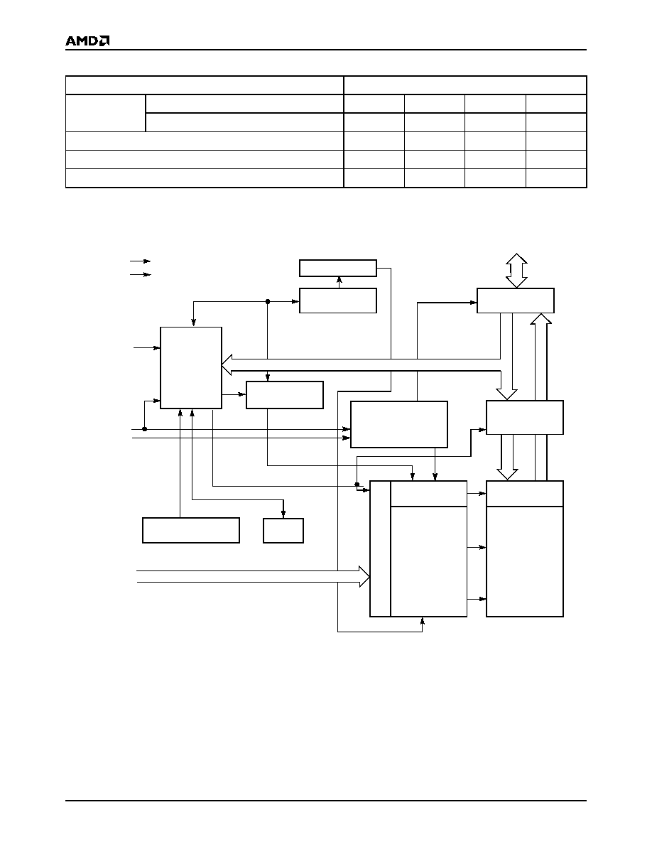
Product Selector Guide . . . . . . . . . . . . . . . . . . . . . 4
Block Diagram . . . . . . . . . . . . . . . . . . . . . . . . . . . . 4
Connection Diagrams . . . . . . . . . . . . . . . . . . . . . . . 5
Pin Configuration . . . . . . . . . . . . . . . . . . . . . . . . . . 6
Logic Symbol . . . . . . . . . . . . . . . . . . . . . . . . . . . . 6
Ordering Information . . . . . . . . . . . . . . . . . . . . . . . 7
Device Bus Operations . . . . . . . . . . . . . . . . . . . . . . 8
Table 1. Am29LV010B Device Bus Operations ................................ 8
Requirements for Reading Array Data ..................................... 8
Writing Commands/Command Sequences .............................. 8
Program and Erase Operation Status ...................................... 9
Standby Mode .......................................................................... 9
Automatic Sleep Mode ............................................................. 9
Output Disable Mode ................................................................ 9
Table 2. Am29LV010B Uniform Sector Address Table..................... 9
Autoselect Mode ..................................................................... 10
Table 3. Am29LV010B Autoselect Codes....................................... 10
Sector Protection/Unprotection ............................................... 10
Hardware Data Protection ...................................................... 10
Low V
CC
Write Inhibit .............................................................. 10
Write Pulse "Glitch" Protection ............................................... 10
Logical Inhibit .......................................................................... 10
Power-Up Write Inhibit ............................................................ 11
Command Definitions . . . . . . . . . . . . . . . . . . . . . 11
Reading Array Data ................................................................ 11
Reset Command ..................................................................... 11
Autoselect Command Sequence ............................................ 11
Byte Program Command Sequence ....................................... 11
Unlock Bypass Command Sequence ..................................... 12
Figure 1. Program Operation ..........................................................12
Chip Erase Command Sequence ........................................... 12
Sector Erase Command Sequence ........................................ 13
Erase Suspend/Erase Resume Commands ........................... 13
Figure 2. Erase Operation ...............................................................14
Command Definitions ............................................................. 15
Table 4. Am29LV010B Command Definitions ................................ 15
Write Operation Status . . . . . . . . . . . . . . . . . . . . . 16
DQ7: Data# Polling ................................................................. 16
Figure 3. Data# Polling Algorithm ...................................................16
DQ6: Toggle Bit I .................................................................... 17
DQ2: Toggle Bit II ................................................................... 17
Reading Toggle Bits DQ6/DQ2 .............................................. 17
Figure 4. Toggle Bit Algorithm .........................................................18
DQ5: Exceeded Timing Limits ................................................ 18
DQ3: Sector Erase Timer ....................................................... 18
Table 5. Write Operation Status..................................................... 19
Absolute Maximum Ratings . . . . . . . . . . . . . . . . 20
Figure 5. Maximum Negative Overshoot Waveform ...................... 20
Figure 6. Maximum Positive Overshoot Waveform ........................ 20
Operating Ranges . . . . . . . . . . . . . . . . . . . . . . . . . 20
DC Characteristics . . . . . . . . . . . . . . . . . . . . . . . . 21
Figure 7. I
CC1
Current vs. Time (Showing Active and Automatic
Sleep Currents) .............................................................................. 22
Figure 8. I
CC1
vs. Frequency .......................................................... 22
Test Conditions . . . . . . . . . . . . . . . . . . . . . . . . . . 23
Figure 9. Test Setup ....................................................................... 23
Table 6. Test Specifications ........................................................... 23
Key to Switching Waveforms. . . . . . . . . . . . . . . . 23
Figure 10. Input Waveforms and Measurement Levels ................. 23
AC Characteristics . . . . . . . . . . . . . . . . . . . . . . . . 24
Read Operations .................................................................... 24
Figure 11. Read Operations Timings ............................................. 24
Erase/Program Operations ..................................................... 25
Figure 12. Program Operation Timings .......................................... 26
Figure 13. Chip/Sector Erase Operation Timings .......................... 27
Figure 14. Data# Polling Timings (During Embedded Algorithms) . 28
Figure 15. Toggle Bit Timings (During Embedded Algorithms) ...... 28
Figure 16. DQ2 vs. DQ6 ................................................................. 29
Figure 17. Alternate CE# Controlled Write Operation Timings ...... 30
Erase and Programming Performance . . . . . . . . 30
Latchup Characteristics . . . . . . . . . . . . . . . . . . . . 31
TSOP Pin Package Capacitance . . . . . . . . . . . . . 31
PLCC Pin Capacitance . . . . . . . . . . . . . . . . . . . . . 31
Data Retention. . . . . . . . . . . . . . . . . . . . . . . . . . . . 31
Physical Dimensions . . . . . . . . . . . . . . . . . . . . . . 32
PL 032--32-Pin Plastic Leaded Chip Carrier ......................... 32
TS 032--32-Pin Standard Thin Small Outline Package ......... 33
TSR032--32-Pin Reverse Thin Small Outline Package ......... 34
Revision Summary . . . . . . . . . . . . . . . . . . . . . . . . 35
Revision A (April 1998) ........................................................... 35
Revision B (September 1998) ................................................. 35
Revision C (January 1999) ..................................................... 35
Revision C+1 (March 22, 1999) .............................................. 35
Revision C+2 (October 5, 1999) ............................................. 35
Revision D (December 2, 1999) ............................................. 35
Revision D+1 (November 13, 2000) ....................................... 35