
ADVANCE INFORMATION
This Data Sheet states AMD's current technical specifications regarding the Products described herein. This Data
Sheet may be revised by subsequent versions or modifications due to changes in technical specifications.
Publication# 25270
Rev: A Amendment/0
Issue Date: October 3, 2001
Refer to AMD's Website (www.amd.com) for the latest information.
Am29LV128M
128 Megabit (8 M x 16-Bit/16 M x 8-Bit) MirrorBit
3.0 Volt-only
Uniform Sector Flash Memory with VersatileI/O
Control
DISTINCTIVE CHARACTERISTICS
ARCHITECTURAL ADVANTAGES
s
Single power supply operation
-- 3 volt read, erase, and program operations
s
Enhanced VersatileI/O
control
-- Device generates data output voltages and tolerates
data input voltages as determined by the voltage on
the V
IO
pin; operates from 1.65 to 3.6 V
s
Manufactured on 0.23 µm MirrorBit process
technology
s
SecSi
(Secured Silicon) Sector region
-- 128-word/256-byte sector for permanent, secure
identification through an 8-word/16-byte random
Electronic Serial Number, accessible through a
command sequence
-- May be programmed and locked at the factory or by
the customer
s
Flexible sector architecture
-- Two hundred fifty-six 32 Kword (64 Kbyte) sectors
s
Compatibility with JEDEC standards
-- Provides pinout and software compatibility for
single-power supply flash, and superior inadvertent
write protection
s
Minimum 100,000 erase cycle guarantee per sector
s
20-year data retention at 125
∞
C
PERFORMANCE CHARACTERISTICS
s
High performance
-- 90 ns access time
-- 25 ns page read times
-- 0.4 s typical sector erase time
-- 5.9 µs typical write buffer word programming time:
16-word/32-byte write buffer reduces overall
programming time for multiple-word updates
-- 4-word/8-byte page read buffer
-- 16-word/32-byte write buffer
s
Low power consumption (typical values at 3.0 V, 5
MHz)
-- 30 mA typical active read current
-- 50 mA typical erase/program current
-- 1 µA typical standby mode current
s
Package options
-- 56-pin TSOP
-- 64-ball Fortified BGA
SOFTWARE & HARDWARE FEATURES
s
Software features
-- Program Suspend & Resume: read other sectors
before programming operation is completed
-- Erase Suspend & Resume: read/program other
sectors before an erase operation is completed
-- Data# polling & toggle bits provide status
-- Unlock Bypass Program command reduces overall
multiple-word or byte programming time
-- CFI (Common Flash Interface) compliant: allows host
system to identify and accommodate multiple flash
devices
s
Hardware features
-- Sector Group Protection: hardware-level method of
preventing write operations within a sector group
-- Temporary Sector Unprotect: V
ID
-level method of
changing code in locked sectors
-- WP#/ACC input accelerates programming time
(when high voltage is applied) for greater throughput
during system production. Protects first or last sector
regardless of sector protection settings
-- Hardware reset input (RESET#) resets device
-- Ready/Busy# output (RY/BY#) detects program or
erase cycle completion

2
Am29LV128M
A D V A N C E I N F O R M A T I O N
GENERAL DESCRIPTION
The Am29LV128M is a 128 Mbit, 3.0 volt single power
supply flash memory devices organized as 8,388,608
words or 16,777,216 bytes. The device has a 16-bit
wide data bus that can also function as an 8-bit wide
data bus by using the BYTE# input. The device can be
programmed either in the host system or in standard
EPROM programmers.
An access time of 90, 100, 110, or 120 ns is available.
Note that each device has a specific operating voltage
range (V
CC
) and an I/O voltage range (V
IO
), as speci-
fied in the
Product Selector Guide
and the
Ordering In-
formation
sections. The device is offered in a 56-pin
TSOP or Fortified BGA package. Each device has
separate chip enable (CE#), write enable (WE#) and
output enable (OE#) controls.
Each device requires only a single 3.0 volt power
supply for both read and write functions. In addition to
a V
CC
input, a high-voltage accelerated program
(WP#/ACC) input provides shorter programming times
through increased current. This feature is intended to
facilitate factory throughput during system production,
but may also be used in the field if desired.
The device is entirely command set compatible with
the JEDEC single-power-supply Flash standard.
Commands are written to the device using standard
microprocessor write timing. Write cycles also inter-
nally latch addresses and data needed for the pro-
gramming and erase operations.
The sector erase architecture allows memory sec-
tors to be erased and reprogrammed without affecting
the data contents of other sectors. The device is fully
erased when shipped from the factory.
Device programming and erasure are initiated through
command sequences. Once a program or erase oper-
ation has begun, the host system need only poll the
DQ7 (Data# Polling) or DQ6 (toggle) status bits or
monitor the Ready/Busy# (RY/BY#) output to deter-
mine whether the operation is complete. To facilitate
programming, an Unlock Bypass mode reduces com-
mand sequence overhead by requiring only two write
cycles to program data instead of four.
The VersatileI/OTM (V
IO
) control allows the host sys-
tem to set the voltage levels that the device generates
at its data outputs and the voltages tolerated at its
data inputs to the same voltage level that is asserted
on the V
IO
pin. This allows the device to operate in a
1.8 V or 3 V system environment as required.
Hardware data protection measures include a low
V
CC
detector that automatically inhibits write opera-
tions during power transitions. The hardware sector
protection feature disables both program and erase
operations in any combination of sectors of memory.
This can be achieved in-system or via programming
equipment.
The Erase Suspend/Erase Resume feature allows
the host system to pause an erase operation in a
given sector to read or program any other sector and
then complete the erase operation. The Program
Suspend/Program Resume feature enables the host
system to pause a program operation in a given sector
to read any other sector and then complete the pro-
gram operation.
The hardware RESET# pin terminates any operation
in progress and resets the device, after which it is then
ready for a new operation. The RESET# pin may be
tied to the system reset circuitry. A system reset would
thus also reset the device, enabling the host system to
read boot-up firmware from the Flash memory device.
T he device reduces power c ons umption in the
standby mode when it detects specific voltage levels
on CE# and RESET#, or when addresses have been
stable for a specified period of time.
The SecSi
(Secured Silicon) Sector provides a
128-word/256-byte area for code or data that can be
permanently protected. Once this sector is protected,
no further changes within the sector can occur.
The Write Protect (WP#/ACC) feature protects the
first or last sector by asserting a logic low on the WP#
pin.
AMD MirrorBit flash technology combines years of
Flash memory manufacturing experience to produce
the highest levels of quality, reliability and cost effec-
tiveness. The device electrically erases all bits within a
sector simultaneously via hot-hole assisted erase. The
data is programmed using hot electron injection.
Am29LV128M
3
A D V A N C E I N F O R M A T I O N
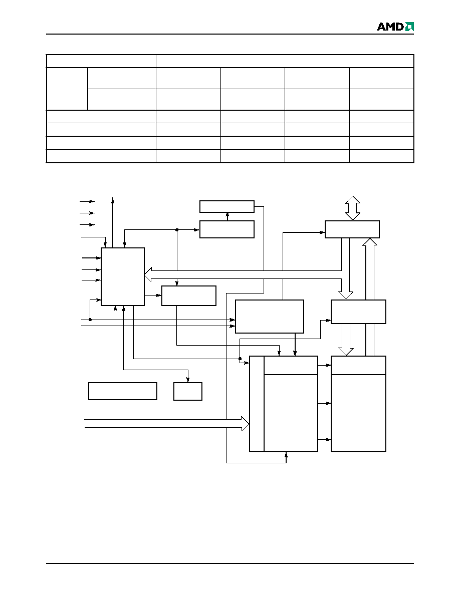
PRODUCT SELECTOR GUIDE
BLOCK DIAGRAM
Part Number
Am29LV128M
Speed
Option
V
CC
= 3.0≠3.6 V
90R
(V
IO
= 3.0≠3.6 V)
V
CC
= 2.7≠3.6 V
101
(V
IO
= 2.7≠3.6 V)
112
(V
IO
= 1.65≠3.6 V)
120
(V
IO
= 1.65≠3.6 V)
Max. Access Time (ns)
90
100
110
120
Max. CE# Access Time (ns)
90
100
110
120
Max. Page access time (t
PACC
)
25
30
40
40
Max. OE# Access Time (ns)
25
30
40
40
Input/Output
Buffers
X-Decoder
Y-Decoder
Chip Enable
Output Enable
Logic
Erase Voltage
Generator
PGM Voltage
Generator
Timer
V
CC
Detector
State
Control
Command
Register
V
CC
V
SS
V
IO
WE#
WP#/ACC
BYTE#
CE#
OE#
STB
STB
DQ0
≠
DQ15 (A-1)
Sector Switches
RY/BY#
RESET#
Data
Latch
Y-Gating
Cell Matrix
A
d
d
r
es
s
Lat
c
h
A22≠A0
4
Am29LV128M
A D V A N C E I N F O R M A T I O N
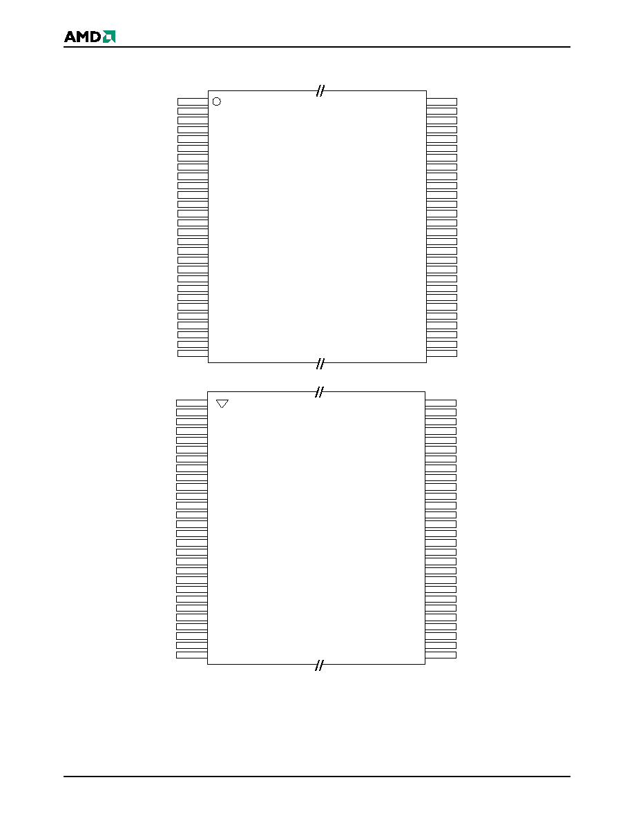
CONNECTION DIAGRAMS
1
2
3
4
5
6
7
8
9
10
11
12
13
14
15
16
17
18
19
20
21
22
NC
A22
A15
A14
A13
A12
A11
A10
A9
A8
A19
A20
WE#
RESET#
A21
WP#/ACC
RY/BY#
A18
A17
A7
A6
A5
56
55
54
53
52
51
50
49
48
47
46
45
44
43
42
41
40
39
38
37
36
35
NC
NC
A16
BYTE#
V
SS
DQ15/A-1
DQ7
DQ14
DQ6
DQ13
DQ5
DQ12
DQ4
V
CC
DQ11
DQ3
DQ10
DQ2
DQ9
DQ1
DQ8
DQ0
23
24
25
26
27
28
A4
A3
A2
A1
NC
NC
34
33
32
31
30
29
OE#
V
SS
CE#
A0
NC
V
IO
56-Pin Standard TSOP
56-Pin Reverse TSOP
Am29LV128M
5
A D V A N C E I N F O R M A T I O N
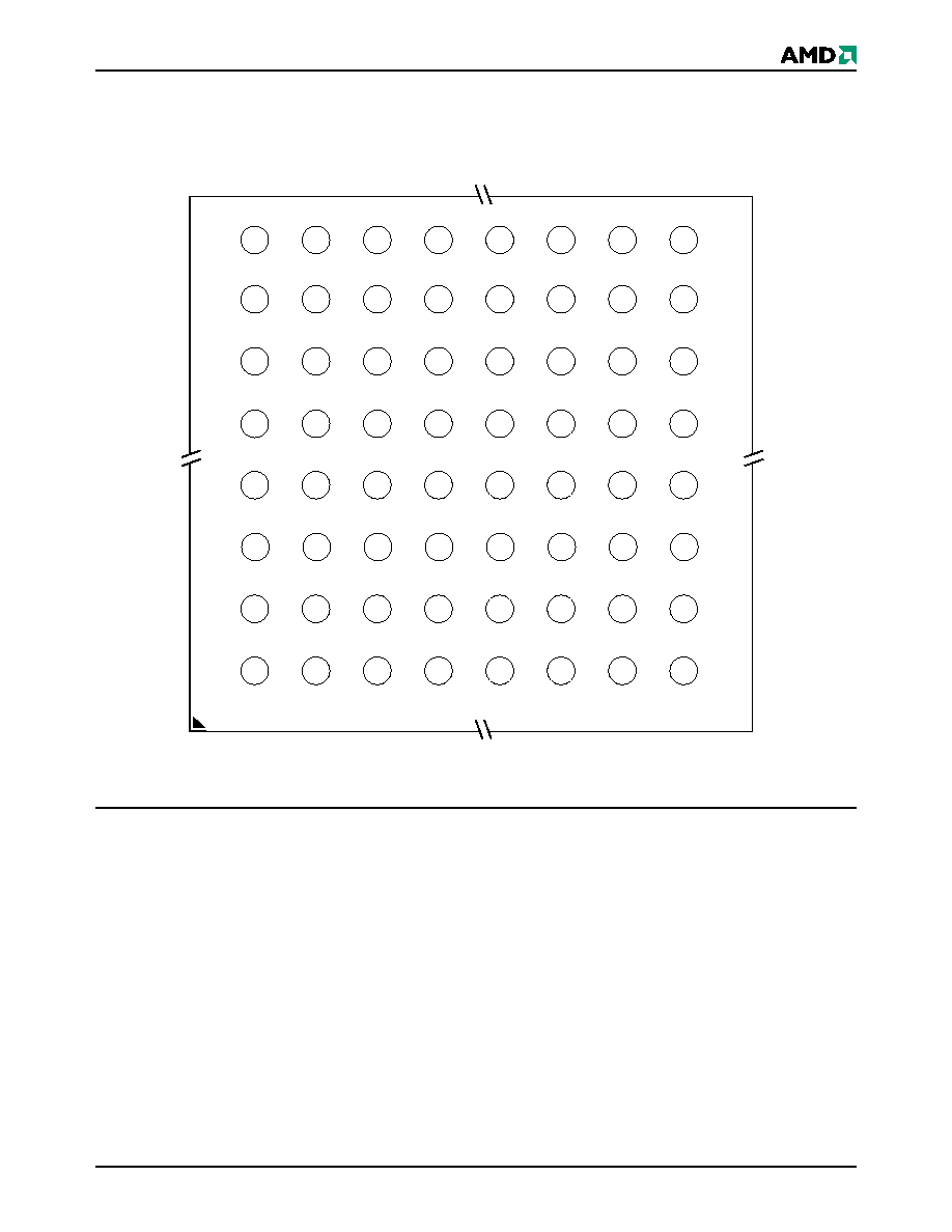
CONNECTION DIAGRAMS
Note: The FBGA package pinout configuration shown is preliminary. The ball count and package physical dimensions have not
yet been determined. Contact AMD for further information.
Special Handling Instructions for FBGA
Package
Special handling is required for Flash Memory products
in FBGA packages.
Flash memory devices in FBGA packages may be
damaged if exposed to ultrasonic cleaning methods.
T h e p a c k a g e a n d / o r d a t a i n t e g r i t y m a y b e
compromised if the package body is exposed to
temperatures above 150
∞
C for prolonged periods of
time.
A2
C2
D2
E2
F2
G2
H2
A3
C3
D3
E3
F3
G3
H3
A4
C4
D4
E4
F4
G4
H4
A5
C5
D5
E5
F5
G5
H5
A6
C6
D6
E6
F6
G6
H6
A7
C7
D7
E7
F7
G7
H7
DQ15/A-1
V
SS
BYTE#
A16
A15
A14
A12
A13
DQ13
DQ6
DQ14
DQ7
A11
A10
A8
A9
V
CC
DQ4
DQ12
DQ5
A19
A21
RESET#
WE#
DQ11
DQ3
DQ10
DQ2
A20
A18
WP#/ACC
RY/BY#
DQ9
DQ1
DQ8
DQ0
A5
A6
A17
A7
OE#
V
SS
CE#
A0
A1
A2
A4
A3
A1
C1
D1
E1
F1
G1
H1
NC
NC
V
IO
NC
NC
NC
NC
NC
A8
C8
B2
B3
B4
B5
B6
B7
B1
B8
D8
E8
F8
G8
H8
NC
NC
NC
V
SS
V
IO
NC
A22
NC
Fortified BGA
Top View, Balls Facing Down
6
Am29LV128M
A D V A N C E I N F O R M A T I O N
PIN DESCRIPTION
A22≠A0
= 23 Address inputs
DQ14≠DQ0 = 15 Data inputs/outputs
DQ15/A-1
= DQ15 (Data input/output, word mode),
A-1 (LSB Address input, byte mode)
CE#
= Chip Enable input
OE#
= Output Enable input
WE#
= Write Enable input
WP#/ACC
= Hardware Write Protect input;
Acceleration input
RESET#
= Hardware Reset Pin input
BYTE#
= Selects 8-bit or 16-bit mode
RY/BY#
= Ready/Busy output
V
CC
= 3.0 volt-only single power supply
(see Product Selector Guide for
speed options and voltage
supply tolerances)
V
IO
= Output Buffer power
V
SS
= Device Ground
NC
= Pin Not Connected Internally
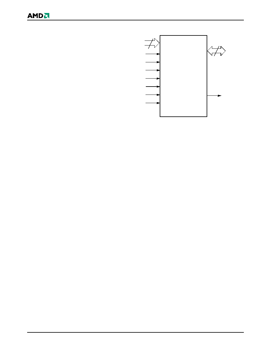
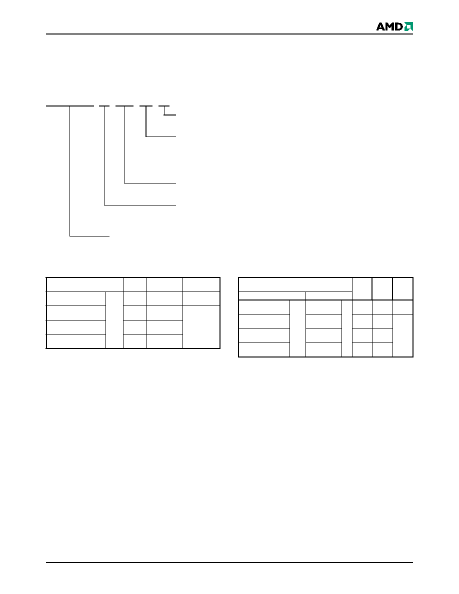
LOGIC SYMBOL
23
16 or 8
DQ15≠DQ0
(A-1)
A22≠A0
CE#
OE#
WE#
RESET#
RY/BY#
WP#/ACC
V
IO
BYTE#
Am29LV128M
7
A D V A N C E I N F O R M A T I O N
ORDERING INFORMATION
Standard Products
AMD standard products are available in several packages and operating ranges. The order number (Valid Combination) is
formed by a combination of the following:
Valid Combinations
Valid Combinations list configurations planned to be supported in vol-
ume for this device. Consult the local AMD sales office to confirm
availability of specific valid combinations and to check on newly re-
leased combinations.
Am29LV128M
H
90R
PC
I
TEMPERATURE RANGE
I =
Industrial
(≠40
∞
C to +85
∞
C)
PACKAGE TYPE
E
=
56-Pin Thin Small Outline Package (TSOP) Standard Pinout (TS 056)
F
=
56-Pin Thin Small Outline Package (TSOP) Reverse Pinout (TSR056)
PC
=
64-Ball Fortified Ball Grid Array (
F
BGA),
13 x 11 mm, 1.0 mm pitch (LAA064)
SPEED OPTION
See Product Selector Guide and Valid Combinations
SECTOR ARCHITECTURE AND SECTOR WRITE PROTECTION (WP# = V
IL
)
H
=
Uniform sector device, highest address sector protected
L
=
Uniform sector device, lowest address sector protected
DEVICE NUMBER/DESCRIPTION
Am29LV128MH/L
256 Megabit (16 M x 16-Bit/32 M x 8-Bit) MirrorBit Uniform Sector Flash Memory with VersatileIO
Control
3.0 Volt-only Read, Program, and Erase
Valid Combinations for
TSOP Package
Speed(
ns)
V
IO
Range
V
CC
Range
Am29LV128MH90R,
Am29LV128ML90R
EI,
FI
90
3.0≠3.6 V
3.0≠3.6 V
Am29LV128MH101,
Am29LV128ML101
100
2.7≠3.6 V
2.7≠3.6 V
Am29LV128MH112,
Am29LV128ML112
110
1.65≠3.6 V
Am29LV128MH120,
Am29LV128ML120
120
1.65≠3.6 V
Valid Combinations for
Fortified BGA Package
Speed
(ns)
V
IO
Range
V
CC
Range
Order Number
Package Marking
Am29LV128MH90R,
Am29LV128ML90R
PCI
L128MH90R,
L128ML90R
I
90
3.0≠
3.6 V
3.0≠
3.6 V
Am29LV128MH101,
Am29LV128ML101
L128MH01V,
L128ML01V
100
2.7≠
3.6 V
2.7≠
3.6 V
Am29LV128MH112,
Am29LV128ML112
L128MH11V,
L128ML11V
110
1.65≠
3.6 V
Am29LV128MH120,
Am29LV128ML120
L128MH12V,
L128ML12V
120
1.65≠
3.6 V
8
Am29LV128M
A D V A N C E I N F O R M A T I O N
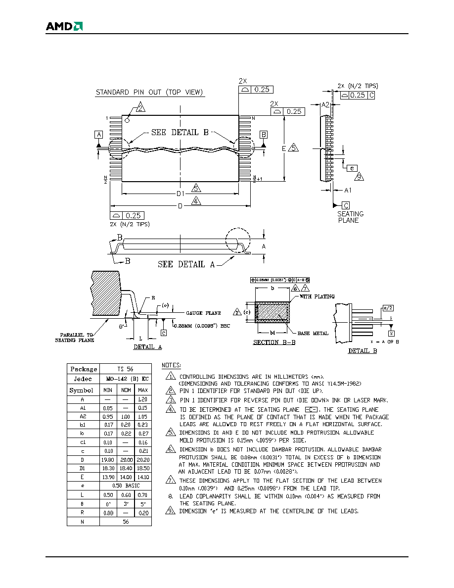
PHYSICAL DIMENSIONS
TS056--56-Pin Standard Thin Small Outline Package (TSOP)

Am29LV128M
9
A D V A N C E I N F O R M A T I O N
PHYSICAL DIMENSIONS
TSR056--56-Pin Reverse Thin Small Outline Package (TSOP)
TBD
10
Am29LV128M
A D V A N C E I N F O R M A T I O N
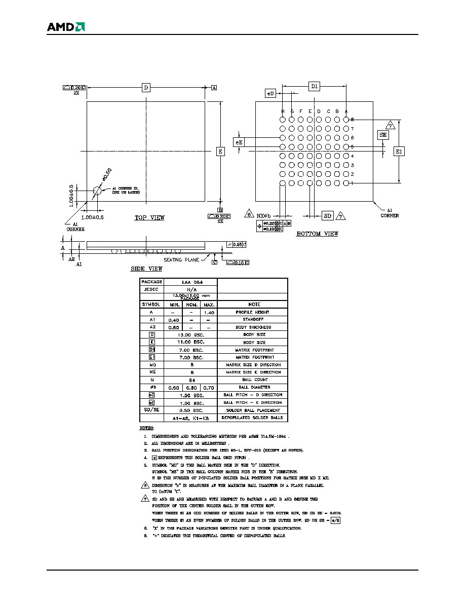
PHYSICAL DIMENSIONS
LAA064--64-Ball Fortified Ball Grid Array (
F
BGA) 13 x 11 mm Package

Am29LV128M
11
A D V A N C E I N F O R M A T I O N
REVISION SUMMARY
Revision A (October 3, 2001)
Initial release as abbreviated Advance Information
data sheet.
Trademarks
Copyright © 2001 Advanced Micro Devices, Inc. All rights reserved.
AMD, the AMD logo, and combinations thereof are registered trademarks of Advanced Micro Devices, Inc.
ExpressFlash is a trademark of Advanced Micro Devices, Inc.
Product names used in this publication are for identification purposes only and may be trademarks of their respective companies.