 | –≠–ª–µ–∫—Ç—Ä–æ–Ω–Ω—ã–π –∫–æ–º–ø–æ–Ω–µ–Ω—Ç: AM79535 | –°–∫–∞—á–∞—Ç—å:  PDF PDF  ZIP ZIP |
Publication# 16854
Rev: D Amendment: /0
Issue Date: October 1999
Am79534/Am79535
Subscriber Line Interface Circuit
DISTINCTIVE CHARACTERISTICS
s
Programmable constant-current feed
s
Line-feed characteristics independent of
battery variations
s
Programmable loop-detect threshold
s
On-chip switching regulator for low-power
dissipation
s
Pin for external ground-key noise-filter
capacitor available
s
Ground-key detect
s
Two-wire impedance set by single external
impedance
s
Polarity reversal feature
s
Tip Open state for ground-start lines
s
Test relay driver optional
s
On-hook transmission
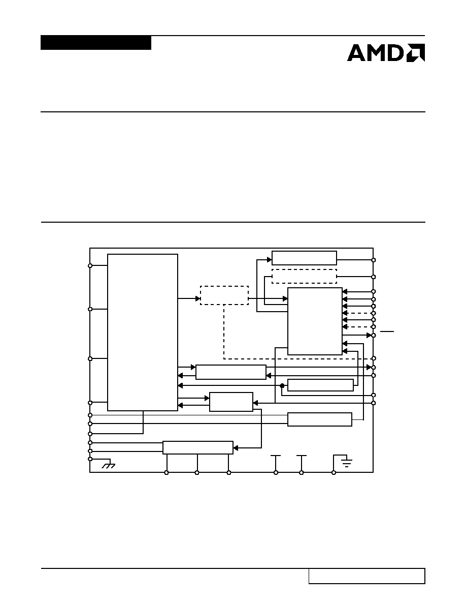
BLOCK DIAGRAM
Two-Wire
Interface
HPA
HPB
DA
DB
BGND
VBAT
A(TIP)
B(RING)
Ground-Key
Detector
Signal Transmission
Power-Feed
Controller
Ring-Trip Detector
VCC
VEE
AGND
RINGOUT
C1
C2
E1
E0
DET
RSN
VTX
RD
RDC
Ring Relay Driver
Input Decoder
and Control
Off-Hook Detector
Test Relay Driver
TESTOUT
C3
C4
GKFIL
Switching Regulator
VREG
L
CHS
QBAT
CHCLK
Notes:
1. Am79534--E0 and E1 inputs; ring and test relay drivers sourced internally to BGND.
2. Am79535--E0 and E1 inputs; ring relay driver sourced internally to BGND; ground-key filter pin.
3. Current gain (K
1
) = 1000 for all parts.
16854C-01
2
Am7953X Data Sheet
ORDERING INFORMATION
Standard Products
AMD standard products are available in several packages and operating ranges. The order number (Valid Combination) is formed
by a combination of the elements below.
Valid Combinations
Valid Combinations list configurations planned to be supported
in volume for this device. Consult the local AMD sales office to
confirm availability of specific valid combinations, to check on
newly released combinations, and to obtain additional data on
AMD's standard military grade products.
Note:
* Functionality of the device from 0
∞
C to +70
∞
C is guaranteed by production testing. Performance from ≠40
∞
C to +85
∞
C is
guaranteed by characterization and periodic sampling of production units.
Am7953X
J
C
PERFORMANCE GRADE
Blank = Standard Specification
≠1 = Performance Grading
≠2 = Performance Grading
OPERATING CONDITIONS
C = Commercial (0
∞
C to 70
∞
C)*
PACKAGE TYPE
J = 32-Pin Plastic-Leaded Chip Carrier (PL 032)
DEVICE NUMBER/DESCRIPTION
Am7953X
Subscriber Line Interface Circuit
Valid Combinations
Am7953X
≠1
≠2
DC
JC

SLIC Products
3
CONNECTION DIAGRAMS
Top View
RDC
VCC
RSVD
RSVD
CHS
L
TESTOUT
VBAT
QBAT
CHCLK
DA
HPB
HPA
VTX
VEE
RD
BGND
B(RING)
A(T
I
P)
DB
4
3
2
1
32
31
30
RINGOUT
C3
8
9
10
11
29
28
27
26
25
24
23
14
15
16
17
18
19
20
E0
C2
Am79534
DET
C1
DG
ND
7
6
5
Notes:
1. Pin 1 is marked for orientation.
2. TP is a thermal conduction pin tied to substrate (QBAT).
3. RSVD = Reserved. Do not connect to these pins.
12
13
22
21
RSN
AGND
C4
E1
VREG
RD
C
VCC
TP
TP
CHS
L
GKFIL
VBAT
QBAT
CHCLK
DA
HPB
HPA
VTX
VEE
RD
BG
ND
B(RI
N
G
)
A(TIP)
DB
4
3
2
1
32
31
30
RI
N
G
O
U
T
C3
8
9
10
11
29
28
27
26
25
24
23
14
15
16
17
18
19
20
E0
C2
Am79535
DET
C1
DGN
D
7
6
5
12
13
22
21
RSN
AGND
RSVD
E1
VREG

4
Am7953X Data Sheet
PIN DESCRIPTIONS
Pin Names
Type
Description
AGND
Gnd
Analog (quiet) ground.
A(TIP)
Output
Output of A(TIP) power amplifier.
BGND
Gnd
Battery (power) ground.
B(RING)
Output
Output of B(RING) power amplifier.
C3≠C1
Input
Decoder. TTL compatible. C3 is MSB and C1 is LSB.
C4
Input
Test relay driver command (Am79534). TTL compatible. A logic Low enables the driver.
CHCLK
Input
Chopper clock. Input to switching regulator (TTL compatible). Frequency = 256 kHz (nominal).
CHS
Input
Chopper stabilization. Connection for external stabilization components.
DA
Input
Ring-trip negative. Negative input to ring-trip comparator.
DB
Input
Ring-trip positive. Positive input to ring-trip comparator.
DET
Output
Detector. A logic Low indicates that the selected detector is tripped. The detector is selected by
the logic inputs (C3≠C1, E0, and E1). The output is open-collector with a built-in 15 k
pull-up
resistor.
DGND
Gnd
Digital ground.
E0
Input
Read enable. A logic High enables DET. A logic Low disables DET.
E1
Input
Ground-key enable. E1 = High connects the ground-key detector to DET, and E1 = Low connects
the off-hook or ring-trip detector to DET.
GKFIL
Capacitor
Ground-key filter capacitor connection ( Am79535). An external capacitor for filtering out
high-frequency noise from the ground-key loop can be connected to this pin. An internal 36 k
, ≠
20%, +40% resistor is provided to form an RC filter with the external capacitor. In versions that
have a GKFIL pin, 3.3 nF minimum capacitance must be connected from the GKFIL pin to ground.
HPA
Capacitor
High-pass filter capacitor; A(TIP) side of high-pass filter capacitor.
HPB
Capacitor
High-pass filter capacitor; B(RING) side of high-pass filter capacitor.
L
Output
Switching regulator power transistor. Connection point for filter inductor and anode of catch diode.
This pin has up to 60 V of pulse waveform on it and must be isolated from sensitive circuits. Keep
the diode connections short because of the high currents and high di/dt.
QBAT
Battery
Quiet battery. Filtered battery supply for the signal processing circuits.
RD
Resistor
Detect resistor. Threshold modification and filter point for the off-hook detector.
RDC
Resistor
DC feed resistor. Connection point for the DC feed-current programming network which also
connects to the Receiver Summing Node (RSN). V
RDC
is negative for normal polarity and
positive for reverse polarity.
RINGOUT
Output
Ring relay driver; sourcing from BGND with internal diode to QBAT.
RSN
Input
Receive summing node. The metallic current ( AC and DC) between A(TIP) and B(RING) is equal
to 1000 times the current into this pin. The networks that program receive gain, two-wire
impedance, and feed current all connect to this node. This node is extremely sensitive. Route the
256 kHz chopper clock and switch lines away from the RSN node.
TESTOUT
Output
Test relay driver (Am79534); sourcing from BGND with internal diode to QBAT.
TP
Thermal
Thermal pin. Connection for heat dissipation. Internally connected to substrate (QBAT). Leave as
open circuit or connected to QBAT. In both cases, the TP pins can connect to an area of copper
on the board to enhance heat dissipation.
VBAT
Battery
Battery supply through an external protection diode.
VCC
Power
+5 V power supply.
VEE
Input
≠5 V power supply.
VREG
Input
Regulated voltage. Provides negative power supply for power amplifiers and connection point for
inductor, filter capacitor, and chopper stabilization.
VTX
Output
Transmit audio. This output is a unity gain version of the A(TIP) and B(RING) metallic voltage. VTX
also sources the two-wire input impedance-programming network connects here.

SLIC Products
5
ABSOLUTE MAXIMUM RATINGS
Storage temperature . . . . . . . . . . . . ≠55
∞
C to +150
∞
C
V
CC
with respect to AGND/DGND . . .≠0.4 V to +7.0 V
V
EE
with respect to AGND/DGND . . .+0.4 V to ≠7.0 V
V
BAT
with respect to AGND/DGND . . +0.4 V to ≠70 V
Note: Rise time of V
BAT
(dv/dt) must be limited to 27 V/
µ
s or
less when Q
BAT
bypass = 0.33
µ
F.
BGND with respect to
AGND/DGND. . . . . . . . . . . . . . . .+1.0 V to ≠3.0 V
A(TIP) or B(RING) to BGND:
Continuous . . . . . . . . . . . . . . . . . ≠70 V to +1.0 V
10 ms (f = 0.1 Hz) . . . . . . . . . . . . ≠70 V to +5.0 V
1
µ
s (f = 0.1 Hz). . . . . . . . . . . . . . .≠90 V to +10 V
250 ns (f = 0.1 Hz) . . . . . . . . . . . .≠120 V to +15 V
Current from A(TIP) or B(RING). . . . . . . . . .
±
150 mA
Voltage on RINGOUT . . . BGND to 70 V above Q
BAT
Voltage on TESTOUT . . . BGND to 70 V above Q
BAT
Current through relay drivers . . . . . . . . . . . . . . 60 mA
Voltage on ring-trip inputs (DA and DB) . . .V
BAT
to 0 V
Current into ring-trip inputs . . . . . . . . . . . . . .
±
10 mA
Peak current into regulator switch (L pin) . . . 150 mA
Switcher transient peak off voltage on L pin . . +1.0 V
C4≠C1, E1, CHCLK to
AGND/DGND. . . . . . . . . . ≠0.4 V to (V
CC
+ 0.4 V)
Maximum power dissipation (see note) . . . T
A
= 70
∞
C
In 32-pin PLCC package . . . . . . . . . . . . . 1.74 W
Note: Thermal limiting circuitry on chip will shut down the
circuit at a junction temperature of about 165
∞
C. The device
should never be exposed to this temperature. Operation
above 145
∞
C junction temperature may degrade device
reliability. See the SLIC Packaging Considerations for more
information.
Stresses above those listed under Absolute Maximum Ratings
may cause permanent device failure. Functionality at or above
these limits is not implied. Exposure to Absolute Maximum
Ratings for extended periods may affect device reliability.
OPERATING RANGES
Commercial (C) Devices
Ambient temperature . . . . . . . . . . . . . . 0
∞
C to +70
∞
C*
V
CC
. . . . . . . . . . . . . . . . . . . . . . . . . . 4.75 V to 5.25 V
V
EE
. . . . . . . . . . . . . . . . . . . . . . . . ≠4.75 V to ≠5.25 V
V
BAT
. . . . . . . . . . . . . . . . . . . . . . . . . . ≠40 V to ≠58 V
AGND/DGND . . . . . . . . . . . . . . . . . . . . . . . . . . . . 0 V
BGND with respect to
AGND/DGND . . . . . . . . . . . ≠100 mV to +100 mV
Load resistance on VTX to ground . . . . . . . 10 k
min
Operating Ranges define those limits between which the
functionality of the device is guaranteed.
* Functionality of the device from 0
∞
C to +70
∞
C is guaranteed
by production testing. Performance from
≠
40
∞
C to +85
∞
C is
guaranteed by characterization and periodic sampling of
production units.
6
Am7953X Data Sheet
ELECTRICAL CHARACTERISTICS
Note:
* P.G. = Performance Grade (≠2 performance parameters are equivalent to ≠1 performance parameters, except where indicated).
Description
Test Conditions (See Note 1)
Min
Typ
Max
Unit
Note
Analog (V
TX
) output impedance
3
4
Analog (V
TX
) output offset
0
∞
C to +70
∞
C
≠1*
≠40
∞
C to +85
∞
C
≠1
≠35
≠30
≠40
≠35
+35
+30
+40
+35
mV
4
4
Analog (RSN) input impedance
300 Hz to 3.4 kHz
1
20
4
Longitudinal impedance at A or B
35
Overload level
Z
2WIN
= 600
to 900
4-wire
2-wire
≠3.1
+3.1
Vpk
2
Transmission Performance, 2-Wire Impedance
2-wire return loss
(See Test Circuit D)
300 Hz to 500 Hz
500 Hz to 2.5 kHz
2.5 kHz to 3.4 kHz
26
26
20
dB
4, 10
Longitudinal Balance (2-Wire and 4-Wire, See Test Circuit C)
R
L
= 600
Longitudinal to metallic L-T, L-4
300 Hz to 3.4 kHz
≠1*
48
52
dB
Longitudinal to metallic L-T, L-4
200 Hz to 1 kHz:
Normal polarity
0
∞
C to +70
∞
C
≠2*
Normal polarity
≠40
∞
C to +85
∞
C
≠2
Reverse polarity
≠2
63
58
54
4
1 kHz to 3.4 kHz:
Normal polarity
0
∞
C to +70
∞
C
≠2*
Normal polarity
≠40
∞
C to +85
∞
C
≠2
Reverse polarity
≠2
58
54
54
4
Longitudinal signal generation 4-L
300 Hz to 800 Hz
300 Hz to 800 Hz
≠1*
40
42
Longitudinal current capability per wire Active state
OHT state
25
18
mArms
4
Insertion Loss (2- to 4-Wire and 4- to 2-Wire, See Test Circuits A and B)
Gain accuracy
0 dBm, 1 kHz
0
∞
C to +70
∞
C
0 dBm, 1 kHz
≠40
∞
C to +85
∞
C
0 dBm, 1 kHz
0
∞
C to +70
∞
C
≠1*
0 dBm, 1 kHz
≠40
∞
C to +85
∞
C
≠1
≠0.15
≠0.20
≠0.1
≠0.15
+0.15
+0.20
+0.1
+0.15
dB
4
4
Variation with frequency
300 Hz to 3.4 kHz
(relative to 1 kHz):
0
∞
C to +70
∞
C
≠40
∞
C to +85
∞
C
≠0.1
≠0.15
+0.1
+0.15
4
Gain tracking
+7 dBm to ≠55 dBm:
0
∞
C to +70
∞
C
≠40
∞
C to +85
∞
C
≠0.1
≠0.15
+0.1
+0.15
4
SLIC Products
7
ELECTRICAL CHARACTERISTICS (continued)
Description
Test Conditions (See Note 1)
Min
Typ
Max
Unit
Note
Balance Return Signal (4- to 4-Wire, See Test Circuit B)
Gain accuracy
0 dBm, 1 kHz
0
∞
C to +70
∞
C
0 dBm, 1 kHz
≠40
∞
C to +85
∞
C
0 dBm, 1 kHz
0
∞
C to +70
∞
C
≠1*
0 dBm, 1 kHz
≠40
∞
C to +85
∞
C
≠1
≠0.15
≠0.20
≠0.1
≠0.15
+0.15
+0.20
+0.1
+0.15
dB
4
4
Variation with frequency
300 Hz to 3.4 kHz
(relative to 1 kHz):
0
∞
C to +70
∞
C
≠40
∞
C to +85
∞
C
≠0.1
≠0.15
+0.1
+0.15
4
Gain tracking
+7 dBm to ≠55 dBm:
0
∞
C to +70
∞
C
≠40
∞
C to +85
∞
C
≠0.1
≠0.15
+0.1
+0.15
4
4
Group delay
f = 1 kHz
5.3
µ
s
4
Total Harmonic Distortion (2- to 4-Wire or 4- to 2-Wire, See Test Circuits A and B)
Total harmonic distortion
0 dBm, 300 Hz to 3.4 kHz
+9 dBm, 300 Hz to 3.4 kHz
≠64
≠55
≠50
≠40
dB
Idle Channel Noise
C-message weighted noise
2-wire:
0
∞
C to +70
∞
C
2-wire:
0
∞
C to +70
∞
C
≠1*
2-wire:
≠40
∞
C to +85
∞
C
+7
+7
+7
+15
+12
+15
dBrnC
4
4-wire
0
∞
C to +70
∞
C
4-wire
0
∞
C to +70
∞
C
≠1*
4-wire
≠40
∞
C to +85
∞
C
+7
+7
+7
+15
+12
+15
4
Psophometric weighted noise
2-wire
0
∞
C to +70
∞
C
2-wire
0
∞
C to +70
∞
C
≠1*
2-wire
≠40
∞
C to +85
∞
C
≠83
≠83
≠83
≠75
≠78
≠75
dBmp
7
4
4-wire
0
∞
C to +70
∞
C
4-wire
0
∞
C to +70
∞
C
≠1*
4-wire
≠40
∞
C to +85
∞
C
≠83
≠83
≠83
≠75
≠78
≠75
7
4
Single Frequency Out-of-Band Noise (See Test Circuit E)
Metallic
4 kHz to 9 kHz
9 kHz to 1 MHz
256 kHz and harmonics
≠76
≠76
≠57
dBm
4, 5, 9
4, 5, 9
4, 5
Longitudinal
1 kHz to 15 kHz
Above 15 kHz
256 kHz and harmonics
≠70
≠85
≠57
4
4, 5, 9
4, 5
DC Feed Currents (See Figure 1) BAT = ≠48 V
Active state loop-current accuracy
I
LOOP
(nominal) = 40 mA
≠7.5
+7.5
%
OHT state
R
L
= 600
18
20
22
mA
Tip Open state
R
L
= 600
1.0
Open Circuit state
R
L
= 0
1.0
Fault current limit, I
L
LIM (I
AX
+ I
BX
)
A and B shorted to GND
130
8
Am7953X Data Sheet
ELECTRICAL CHARACTERISTICS (continued)
Description
Test Conditions (See Note 1)
Min
Typ
Max
Unit
Note
Power Dissipation BAT = ≠48 V, Normal Polarity
On-hook Open Circuit state
≠1*
35
35
120
80
mW
On-hook OHT state
≠1*
135
135
250
200
On-hook Active state
≠1*
200
200
400
300
Off-hook OHT state
R
L
= 600
500
750
Off-hook Active state
R
L
= 600
650
1000
Supply Currents
V
CC
on-hook supply current
Open Circuit state
OHT state
Active state
3.0
6.0
7.5
4.5
10.0
12.0
mA
V
EE
on-hook supply current
Open Circuit state
OHT state
Active state
1.0
2.2
2.7
2.3
3.5
6.0
V
BAT
on-hook supply current
Open Circuit state
OHT state
Active state
0.4
3.0
4.0
1.0
5.0
6.0
Power Supply Rejection Ratio (V
RIPPLE
= 50 mVrms)
V
CC
50 Hz to 3.4 kHz
≠1*
25
30
45
45
dB
6, 7
3.4 kHz to 50 kHz
≠1
22
25
35
35
V
EE
50 Hz to 3.4 kHz
≠1*
20
25
40
40
3.4 kHz to 50 kHz
≠1
10
10
25
25
V
BAT
50 Hz to 3.4 kHz
≠1*
27
30
45
45
3.4 kHz to 50 kHz
≠1
20
25
40
40
Off-Hook Detector
Current threshold accuracy
I
DET
= 365/R
D
nominal
≠20
+20
%
Ground-Key Detector Thresholds, Active State, BAT = ≠48 V (See Test Circuit F)
Ground-key resistance threshold
B(RING) to GND
2.0
5.0
10.0
k
Ground-key current threshold
B(RING) to GND
Midpoint to GND
9
mA
8
Ring-Trip Detector Input
Bias current
≠5
≠0.05
µ
A
Offset voltage
Source resistance 0 to 2 M
≠50
0
+50
mV
11

SLIC Products
9
ELECTRICAL CHARACTERISTICS (continued)
RELAY DRIVER SCHEMATICS
Description
Test Conditions (See Note 1)
Min
Typ
Max
Unit
Note
Logic Inputs (C4≠C1, E0, E1, and CHCLK)
Input High voltage
2.0
V
Input Low voltage
0.8
Input High current
All inputs except E1
Input E1
≠75
≠75
40
45
µ
A
Input Low current
≠0.4
mA
Logic Output (DET)
Output Low voltage
I
OUT
= 0.8 mA
0.4
V
Output High voltage
I
OUT
= ≠0.1 mA
2.4
Relay Driver Outputs (RINGOUT, TESTOUT)
On voltage
50 mA source
BGND ≠ 2
BGND ≠
0.95
V
Off leakage
0.5
100
µ
A
Clamp voltage
50 mA sink
Q
BAT
≠ 2
V
TESTOUT
Q
BAT
BGND
Am79534/Am79535
Am79534
16854C-03
RINGOUT
Q
BAT
BGND

10
Am7953X Data Sheet
SWITCHING CHARACTERISTICS
Am79534/Am79535
Symbol
Parameter
Test Conditions
Temperature
Range
Min
Typ
Max
Unit
Note
tgkde
E1 Low to DET High (E0 = 1)
E1 Low to DET Low (E0 = 1)
Ground-key Detect state
R
L
open, R
G
connected
(See Figure H)
0
∞
C to +70
∞
C
≠40
∞
C to +85
∞
C
0
∞
C to +70
∞
C
≠40
∞
C to +85
∞
C
3.8
4.0
1.1
1.6
µ
s
4
tgkdd
E0 High to DET Low (E1 = 0)
0
∞
C to +70
∞
C
≠40
∞
C to +85
∞
C
1.1
1.6
tgkd0
E0 Low to DET High (E1 = 0)
0
∞
C to +70
∞
C
≠40
∞
C to +85
∞
C
3.8
4.0
tshde
E1 High to DET Low (E0 = 1)
E1 High to DET High (E0 = 1)
Switchhook Detect state
R
L
= 600
, R
G
open
(See Figure G)
0
∞
C to +70
∞
C
≠40
∞
C to +85
∞
C
0
∞
C to +70
∞
C
≠40
∞
C to +85
∞
C
1.2
1.7
3.8
4.0
tshdd
E0 High to DET Low (E1 = 1)
0
∞
C to +70
∞
C
≠40
∞
C to +85
∞
C
1.1
1.6
tshd0
E0 Low to DET High (E1 = 1)
0
∞
C to +70
∞
C
≠40
∞
C to +85
∞
C
3.8
4.0

SLIC Products
11
SWITCHING WAVEFORMS
Am79534/Am79535
Notes:
1. Unless otherwise noted, test conditions are BAT = ≠48 V, V
CC
= +5 V, V
EE
= ≠5 V, R
L
= 600
, C
HP
= 0.22
µ
F,
R
DC1
= R
DC2
= 31.25 k
, C
DC
= 0.1
µ
F, R
D
= 51.1 k
, no fuse resistors, two-wire AC output impedance, programming
impedance (Z
T
) = 600 k
resistive, receive input summing impedance (Z
RX
) = 300 k
resistive. (See Table 2 for component
formulas.)
2. Overload level is defined when THD = 1%.
3. Balance return signal is the signal generated at V
TX
by V
RX
. This specification assumes the two-wire AC load impedance
matches the impedance programmed by Z
T
.
4. Not tested in production. This parameter is guaranteed by characterization or correlation to other tests.
5. These tests are performed with a longitudinal impedance of 90
and metallic impedance of 300
for frequencies below
12 kHz and 135
for frequencies greater than 12 kHz. These tests are extremely sensitive to circuit board layout.
6. This parameter is tested at 1 kHz in production. Performance at other frequencies is guaranteed by characterization.
7. When the SLIC is in the Anti-sat 2 operating region, this parameter is degraded. The exact degradation depends on system
design. The Anti-sat 2 region occurs at high loop resistances when |V
BAT
| ≠ |V
AX
≠ V
BX
| is less than approximately 11 V.
8. "Midpoint" is defined as the connection point between two 300
series resistors connected between A(TIP) and B(RING).
9. Fundamental and harmonics from 256 kHz switch-regulator chopper are not included.
10. Assumes the following Z
T
network:
DET
tgkde
DET
tshdd
Note:
All delays measured at 1.4 V level.
E1
E1
E0
E1 to DET
E0 to DET
tshde
tgkde
tshde
tshd0
tgkdd
tgkd0
16854C-02
VTX
RSN
300 k
300 k
30 pF
12
Am7953X Data Sheet
11. Tested with 0
source impedance. 2 M
is specified for system design purposes only.
12. Group delay can be reduced considerably by using a Z
T
network such as that shown in Note 10 above. The network reduces
the group delay to less than 2
µ
s. The effect of group delay on linecard performance may be compensated for by using
QSLACTM or DSLACTM devices.
Note:
* For the Am79534 and Am79535, a logic Low on E0 disables the DET output into the open-collector state.
Table 1.
SLIC Decoding
DET Output (E0 = 1*)
State
C3 C2 C1
Two-Wire Status
E1 = 0
E1 = 1
0
0
0
1
Open Circuit
Ring trip
Ring trip
1
0
0
1
Ringing
Ring trip
Ring trip
2
0
1
0
Active
Loop detector
Ground key
3
0
1
1
On-hook TX (OHT)
Loop detector
Ground key
4
1
0
0
Tip Open
Loop detector
--
5
1
0
1
Reserved
Loop detector
--
6
1
1
0
Active Polarity Reversal
Loop detector
Ground key
7
1
1
1
OHT Polarity Reversal
Loop detector
Ground key

SLIC Products
13
Table 2.
User-Programmable Components
Where Z
T
is connected between the VTX and RSN pins. The
fuse resistors are R
F
, and Z
2WIN
is the desired 2-wire AC input
impedance. When computing Z
T
, the internal current amplifier
pole and any external stray capacitance between VTX and
RSN must be taken into account.
Where Z
RX
is connected from V
RX
to the RSN pin, Z
T
is
defined above, and G
42L
is the desired receive gain.
Where R
DC1
, R
DC2
, and C
DC
form the network connected to
the RDC pin. R
DC1
and R
DC2
are approximately equal.
Where R
D
and C
D
form the network connected from RD to ≠5 V
and I
T
is the threshold current between on hook and off hook.
Z
T
1000 Z
2W IN
2R
F
≠
(
)
=
Z
RX
Z
L
G
42L
------------
1000
Z
T
∑
Z
T
1000 Z
L
2R
F
+
(
)
+
-----------------------------------------------------
∑
=
R
DC 1
R
DC2
+
2500
I
FEED
--------------
=
C
DC
1.5 ms
R
DC 1
R
DC2
+
R
DC 1
R
DC2
∑
---------------------------------
∑
=
R
D
365
I
T
---------,
=
C
D
0.5 ms
R
D
----------------
=

14
Am7953X Data Sheet
DC FEED CHARACTERISTICS
a. V
A
≠V
B
(V
AB
) Voltage vs. Loop Current (Typical)
Notes:
1. Constant-current region:
Active state:
OHT state:
2. Anti-sat turn-on (Active state):
Anti-sat ≠1:
Anti-sat ≠2:
3. Open Circuit voltage (Active state):
4. Anti-sat ≠1 region:
5. Anti-sat ≠2 region:
I
L
2500
R
DC
------------
=
I
L
1
2
---
2500
R
DC
------------
∑
=
V
AB
29.95 V
=
V
AB
1.082 V
BAT
15.149
≠
=
V
AB
0.9 V
BAT
4.995,
≠
=
V
AB
46.25 V,
=
V
BAT
56.9 V
<
V
BAT
56.9 V
V
AB
46.25
I
L
R
DC
150.6
-------------
≠
=
V
AB
0.9 V
BAT
4.995
≠
I
L
R
DC
1128
------------
≠
=
3
5
1
2
4
V
BAT
= ≠50 V
V
BAT
= ≠47.3 V
R
DC
= 62.5 k
Active state
OHT state
2

SLIC Products
15
DC FEED CHARACTERISTICS (continued)
R
DC
= 62.5 k
V
BAT
= ≠47.3 V
b. Loop Current vs. Load Resistance (Typical)
A
B
I
L
RSN
RDC
R
DC1
R
DC2
C
DC
SLIC
R
L
a
b
Feed current programmed by R
DC1
and R
DC2
c. Feed Programming
Figure 1.
DC Feed Characteristics

16
Am7953X Data Sheet
TEST CIRCUITS
I
L2-4
= ≠20 log (V
TX
/ V
AB
)
A. Two- to Four-Wire Insertion Loss
V
AB
R
L
2
R
L
2
A(TIP)
B(RING)
VTX
RSN
AGND
SLIC
V
AB
A(TIP)
B(RING)
VTX
RSN
AGND
SLIC
R
L
I
L4-2
= ≠20 log (V
AB
/ V
RX
)
BRS = 20 log (V
TX
/ V
RX
)
B. Four- to Two-Wire Insertion Loss and Balance Return Signal
R
T
R
T
R
RX
R
RX
V
RX
V
L
V
AB
A(TIP)
B(RING)
VTX
RSN
AGND
SLIC
V
L
S2 Open, S1 Closed:
L-T Long. Bal. = 20 log (V
AB
/ V
L
)
L-4 Long. Bal. = 20 log (V
TX
/ V
L
)
S2 Closed, S1 Open:
4-L Long. Sig. Gen. = 20 log (V
L
/ V
RX
)
C. Longitudinal Balance
R
T
R
RX
V
RX
S2
R
L
2
R
L
2
S1
V
L
C
Note:
Z
D
is the desired impedance (e.g., the
characteristic impedance of the line).
R
L
= ≠20 log (2 V
M
/ V
S
)
V
M
A(TIP)
B(RING)
VTX
RSN
AGND
SLIC
R
T
R
RX
V
S
900
R
R
Z
IN
D. Two-Wire Return Loss Test Circuit
1
C
<< R
L
I
DC

SLIC Products
17
TEST CIRCUITS (continued)
G. Loop-Detector Switching
V
CC
A(TIP)
B(RING)
DET
E1
6.2 k
R
L
= 600
15 pF
A(TIP)
B(RING)
RG = 2 k
H. Ground-Key Switching
E0
A(TIP)
B(RING)
SLIC
68
56
I
DC
68
C
C
1
C
<< 90
E. Single-Frequency Noise
R
L
R
L
R
E
S
E
S
M
A(TIP)
B(RING)
Current Feed or Ground Key
F. Ground-Key Detection
18
Am7953X Data Sheet
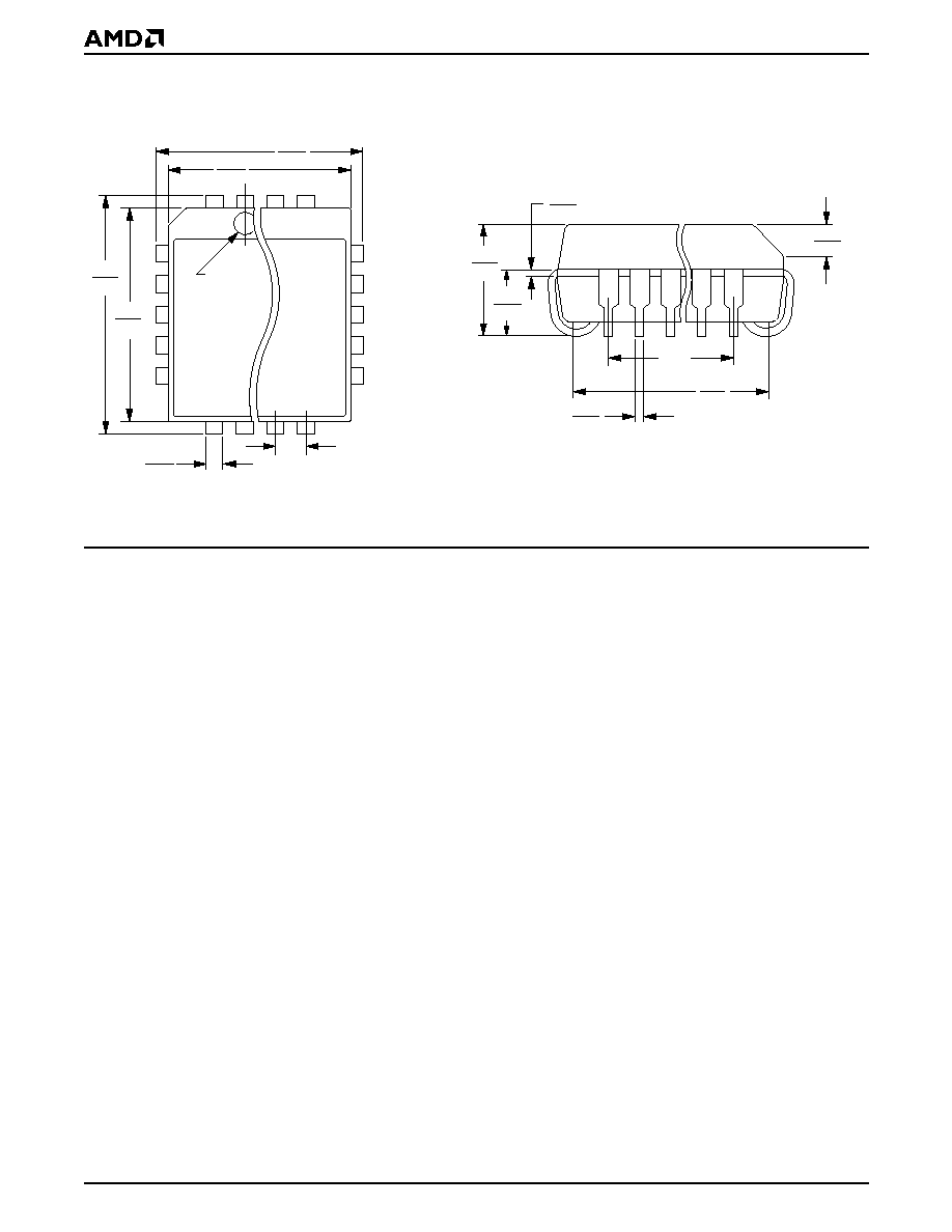
PHYSICAL DIMENSION
PL032
REVISION SUMMARY
Revision B to Revision C
∑
Minor changes to the data sheet style and format were made to conform to AMD standards.
∑
Connection Diagrams--Changed pin 29 from TP to RSVD in the Am79534 diagram.
Revision C to Revision D
∑
In Table 1, SLIC Decoding, the Open Circuit state of 001 was changed to 000.
∑
In Pin Description table, inserted/changed TP pin description to: "Thermal pin. Connection for heat dissipation.
Internally connected to substrate (QBAT). Leave as open circuit or connected to QBAT. In both cases, the TP
pins can connect to an area of copper on the board to enhance heat dissipation."
∑
Minor changes to the data sheet style and format were made to conform to AMD standards.
Revision D to Revision E
∑
The physical dimension (PL032) was added to the Physical Dimension section.
∑
Deleted the Ceramic DIP and Plastic DIP parts (Am79530 and Am79531) and references to them.
∑
Updated Pin Desciption to correct inconsistencies.
.050 REF.
.026
.032
TOP VIEW
Pin 1 I.D.
.485
.495
.447
.453
.585
.595
.547
.553
16-038FPO-5
PL 032
DA79
6-28-94 ae
SIDE VIEW
SEATING
PLANE
.125
.140
.009
.015
.080
.095
.042
.056
.013
.021
.400
REF.
.490
.530

SLIC Products
19
The contents of this document are provided in connection with Advanced Micro Devices, Inc. ("AMD") products. AMD makes no representations
or warranties with respect to the accuracy or completeness of the contents of this publication and reserves the right to make changes to speci-
fications and product descriptions at any time without notice. No license, whether express, implied, arising by estoppel or otherwise, to any in-
tellectual property rights is granted by this publication. Except as set forth in AMD's Standard Terms and Conditions of Sale, AMD assumes no
liability whatsoever, and disclaims any express or implied warranty, relating to its products including, but not limited to, the implied warranty of
merchantability, fitness for a particular purpose, or infringement of any intellectual property right.
AMD's products are not designed, intended, authorized or warranted for use as components in systems intended for surgical implant into the
body, or in other applications intended to support or sustain life, or in any other application in which the failure of AMD's product could create a
situation where personal injury, death, or severe property or environmental damage may occur. AMD reserves the right to discontinue or make
changes to its products at any time without notice.
© 1999 Advanced Micro Devices, Inc.
All rights reserved.
Trademarks
AMD, the AMD logo and combinations thereof are trademarks of Advanced Micro Devices, Inc.
Product names used in this publication are for identification purposes only and may be trademarks of their respective companies.
