 | –≠–ª–µ–∫—Ç—Ä–æ–Ω–Ω—ã–π –∫–æ–º–ø–æ–Ω–µ–Ω—Ç: AME8801 | –°–∫–∞—á–∞—Ç—å:  PDF PDF  ZIP ZIP |
Analog Microelectronics, Inc.
1
AME8801/8812/8840
300mA CMOS LDO
n
n
n
n
n
Typical Application
n
n
n
n
n
Functional Block Diagram
n
n
n
n
n
Features
l
Very Low Dropout Voltage
l
Guaranteed 300mA Output
l
Accurate to within 1.5%
l
30
µ
A Quiescent Current
l
Over-Temperature Shutdown
l
Current Limiting
l
Short Circuit Current Fold-back
l
Noise Reduction Bypass Capacitor
l
Power-Saving Shutdown Mode
l
Space-Saving SOT-25 (SOT-23-5) Package
l
Factory Pre-set Output Voltages
l
Low Temperature Coefficient
n
n
n
n
n
General Description
The AME8801/8840 family of positive, linear regulators
feature low quiescent current (30
µ
A typ.) with low drop-
out voltage, making them ideal for battery applications.
The space-saving SOT-23-5 package is attractive for
"Pocket" and "Hand Held" applications.
These rugged devices have both Thermal Shutdown,
and Current Fold-back to prevent device failure under
the "Worst" of operating conditions.
In applications requiring a low noise, regulated supply,
place a 1000 pF capacitor between Bypass and Ground.
The AME8801 is stable with an output capacitance of
2.2
µ
F or greater.
n
n
n
n
n
Applications
l
Instrumentation
l
Portable Electronics
l
Wireless Devices
l
Cordless Phones
l
PC Peripherals
l
Battery Powered Widgets
l
Electronic Scales
A M P
G N D
O U T
I N
R 1
R 2
V
ref
= 1 . 2 1 5 V
B Y P
Overcurrent
Shutdown
Thermal
Shutdown
E N
A M E 8 8 0 1
O U T P U T
I N P U T
C 3
2.2
µ
F
C 1
1
µ
F
G N D
O U T
5 V
E N
B Y P
IN
C 2
1 n F
Analog Microelectronics, Inc.
2
300mA CMOS LDO
AME8801/8812/8840
n
n
n
n
n
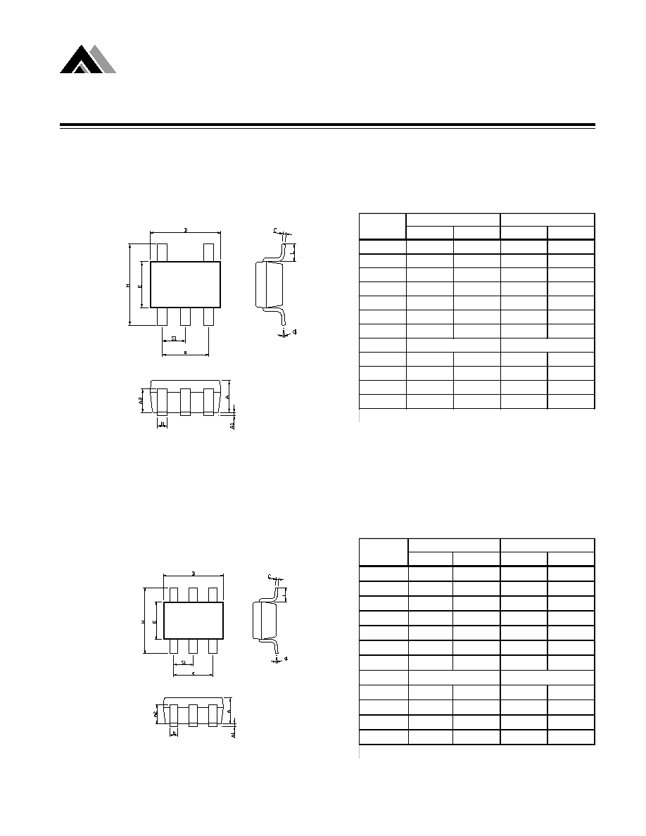
Pin Configuration
1. V
IN
4. BYP
2. GND
5. OUT
3. EN
n
n
n
n
n
Ordering Information
A M E 8 8 0 1
S O T - 2 5 T o p V i e w
1
3
2
5
4
A M E 8 8 4 0
SOT-25 Top View
1
3
2
5
4
1. EN
4. OUT
2. GND
5. V
IN
3. BYP
A M E 8 8 1 2
SOT-25 Top View
1
3
2
5
4
1. EN
4. OUT
2. GND
5. BYP
3. V
IN
A M E 8 8 0 1
SOT-26 Top View
1
3
2
6
4
5
1. OUT
_
1
4. EN
2. GND
5. V
IN
3. BYP 6. OUT_2
Part Number
Marking
Output Voltage
Package
Operating Temp. Range
AME8801AEEV
AAFww
3.3V
SOT-25
-40
O
C to +85
O
C
AME8801BEEV
AAGww
3.0V
SOT-25
-40
O
C to +85
O
C
AME8801CEEV
AAHww
2.8V
SOT-25
-40
O
C to +85
O
C
AME8801DEEV
AAIww
2.5V
SOT-25
-40
O
C to +85
O
C
AME8801EEEV
AAJww
3.8V
SOT-25
-40
O
C to +85
O
C
AME8801FEEV
ABOww
3.6V
SOT-25
-40
O
C to +85
O
C
AME8801GEEV
ACFww
3.5V
SOT-25
-40
O
C to +85
O
C
AME8801HEEV
AEGww
2.7V
SOT-25
-40
O
C to +85
O
C
AME8801IEEV
AEOww
3.4V
SOT-25
-40
O
C to +85
O
C
AME8801JEEV
AGQww
2.85V
SOT-25
-40
O
C to +85
O
C
AME8801KEEV
AHSww
3.7V
SOT-25
-40
O
C to +85
O
C
AME8801LEEV
AJOww
1.5V
SOT-25
-40
O
C to +85
O
C
AME8801MEEV
AJPww
1.8V
SOT-25
-40
O
C to +85
O
C
AME8801NEEV
AKOww
2.9V
SOT-25
-40
O
C to +85
O
C
AME8801OEEV
AKPww
3.1V
SOT-25
-40
O
C to +85
O
C
AME8801SEEV
AQXww
5.0V
SOT-25
-40
O
C to +85
O
C
AME8801JEEY
ARUww
2.85V
SOT-26
-40
O
C to +85
O
C
Please consult AME sales office or authorized Rep./Distributor for other output
voltage and package type availability.
Analog Microelectronics, Inc.
3
AME8801/8812/8840
300mA CMOS LDO
Part Number
Output Voltage
Package
Operating Temp. Range
AME8812AEEV
3.3V
SOT-25
-40
O
C to +85
O
C
AME8812BEEV
3.0V
SOT-25
-40
O
C to +85
O
C
AME8812CEEV
2.8V
SOT-25
-40
O
C to +85
O
C
AME8812DEEV
2.5V
SOT-25
-40
O
C to +85
O
C
AME8812EEEV
3.8V
SOT-25
-40
O
C to +85
O
C
AME8812FEEV
3.6V
SOT-25
-40
O
C to +85
O
C
AME8812GEEV
3.5V
SOT-25
-40
O
C to +85
O
C
AME8812HEEV
2.7V
SOT-25
-40
O
C to +85
O
C
AME8812IEEV
3.4V
SOT-25
-40
O
C to +85
O
C
AME8812JEEV
2.85V
SOT-25
-40
O
C to +85
O
C
AME8812KEEV
3.7V
SOT-25
-40
O
C to +85
O
C
AME8812LEEV
1.5V
SOT-25
-40
O
C to +85
O
C
AME8812MEEV
1.8V
SOT-25
-40
O
C to +85
O
C
AME8812NEEV
2.9V
SOT-25
-40
O
C to +85
O
C
AME8812OEEV
3.1V
SOT-25
-40
O
C to +85
O
C
Please consult AME sales office or authorized Rep./Distributor for other output
voltage and package type availability.
n
n
n
n
n
Ordering Information
Analog Microelectronics, Inc.
4
300mA CMOS LDO
AME8801/8812/8840
n
n
n
n
n
Ordering Information
Part Number
Marking
Output Voltage
Package
Operating Temp. Range
AME8840AEEV
ALCww
3.3V
SOT-25
-40
O
C to +85
O
C
AME8840BEEV
ALDww
3.0V
SOT-25
-40
O
C to +85
O
C
AME8840CEEV
ALEww
2.8V
SOT-25
-40
O
C to +85
O
C
AME8840DEEV
ALFww
2.5V
SOT-25
-40
O
C to +85
O
C
AME8840EEEV
ALGww
3.8V
SOT-25
-40
O
C to +85
O
C
AME8840FEEV
ALHww
3.6V
SOT-25
-40
O
C to +85
O
C
AME8840GEEV
ALIww
3.5V
SOT-25
-40
O
C to +85
O
C
AME8840HEEV
ALJww
2.7V
SOT-25
-40
O
C to +85
O
C
AME8840IEEV
ALKww
3.4V
SOT-25
-40
O
C to +85
O
C
AME8840JEEV
ALLww
2.85V
SOT-25
-40
O
C to +85
O
C
AME8840KEEV
ALMww
3.7V
SOT-25
-40
O
C to +85
O
C
AME8840LEEV
ALNww
1.5V
SOT-25
-40
O
C to +85
O
C
AME8840MEEV
ALOww
1.8V
SOT-25
-40
O
C to +85
O
C
AME8840NEEV
ALPww
2.9V
SOT-25
-40
O
C to +85
O
C
AME8840OEEV
ALQww
3.1V
SOT-25
-40
O
C to +85
O
C
Please consult AME sales office or authorized Rep./Distributor for other output
voltage and package type availability.
Analog Microelectronics, Inc.
5
AME8801/8812/8840
300mA CMOS LDO
n
n
n
n
n
Absolute Maximum Ratings
n
n
n
n
n
Recommended Operating Conditions
n
n
n
n
n
Thermal Information
Caution: Stress above the listed absolute rating may cause permanent damage to the device
Ma x im um
Unit
Thermal Resistance (q
ja
)
SOT-25
260
o
C / W
Internal Power Dissipation (P
D
)
(DT = 100
o
C)
SOT-25
380
mW
Thermal Resistance (q
ja
)
SOT-26
260
o
C / W
Internal Power Dissipation (P
D
)
(DT = 100
o
C)
SOT-26
380
mW
150
o
C
Maximum Junction Temperature
Pa ra m e te r
Pa ra mete r
Ma ximum
Unit
Input Voltage
8
V
Output Current
P
D
/ (V
IN
- V
O
)
mA
Output Voltage
GND - 0.3 to V
IN
+ 0.3
V
ESD Classification
B
Pa ra mete r
Ra ting
Unit
Ambient Temperature Range
-40 to +85
o
C
Junction Temperature
-40 to +125
o
C

Analog Microelectronics, Inc.
6
300mA CMOS LDO
AME8801/8812/8840
n
n
n
n
n
Electronic Specifications
Parameter
Symbol
Min
Typ
Max
Units
Input Voltage
V
IN
Note 1
7
V
Output Voltage Accuracy
V
O
-1.5
1.5
%
1.2V<V
O(NOM)
<=2.0V
1300
Dropout Voltage
V
DROPOUT
2.0V<V
O(NOM)
<=2.8V
400
2.8V<V
O(NOM)
300
Output Current
I
O
300
mA
Current Limit
I
LIM
300
450
mA
Short Circuit Current
I
SC
150
300
mA
Quiescent Current
I
Q
30
50
µ
A
Ground Pin Current
I
GND
35
µ
A
V
O
< 2.0V
-0.15
0.15
%
2.0V<=V
O
< 4.0V
-0.1
0.02
0.1
%
4.0V <= Vo
-0.4
0.2
0.4
%
Load Regulation
REG
LOAD
-1
0.2
1
%
Over Temerature Shutdown
OTS
150
o
C
Over Temerature Hysterisis
OTH
30
o
C
V
O
Temperature Coefficient
TC
30
ppm/
o
C
f=1kHz
50
PSRR
f=10kHz
20
dB
f=100kHz
15
V
EH
2.0
Vin
V
V
EL
0
0.4
V
I
EH
0.1
µ
A
I
EL
0.5
µ
A
Shutdown Supply Current
I
SD
0.5
1
µ
A
Shutdown Output Voltage
V
O,SD
0
0.4
V
Note1:V
IN(min)
=V
OUT
+V
DROPOUT
TA = 25
o
C unless otherwise noted
Test Condition
I
O
=1mA
V
O
<0.8V
I
O
=0mA
I
O
=1mA to 300mA
Line Regulation
REG
LINE
I
O
=1mA
V
IN
=V
O
+1 to V
O
+2
EN Input Threshold
V
IN
=2.7V to 7V
V
IN
=2.7V to 7V
EN Input Bias Current
V
EN
=V
IN
, V
IN
=2.7V to 7V
V
EN
=0V, V
IN
=2.7V to 7V
See
chart
mV
V
O
>1.2V
V
O
>1.2V
I
O
=300mA
V
O
=V
ONOM
-2.0%
I
O
=1mA to 300mA
µ
Vrms
Power Supply Rejection
I
O
=100mA
C
O
=2.2
µ
F
Output Voltage Noise
eN
f=10Hz to 100kHz
I
O
=10mA
Co=2.2
µ
F
V
IN
=5V, V
O
=0V, V
EN
<V
EL
I
O
=0.4mA, V
EN
<V
EL
30

Analog Microelectronics, Inc.
7
AME8801/8812/8840
300mA CMOS LDO
n
n
n
n
n
Detailed Description
The AME8801/8840 family of CMOS regulators contain
a PMOS pass transistor, voltage reference, error ampli-
fier, over-current protection, and thermal shutdown.
The P-channel pass transistor receives data from the
error amplifier, over-current shutdown, and thermal pro-
tection circuits. During normal operation, the error am-
plifier compares the output voltage to a precision refer-
ence. Over-current and Thermal shutdown circuits be-
come active when the junction temperature exceeds
150
o
C, or the current exceeds 300mA. During thermal
shutdown, the output voltage remains low. Normal op-
eration is restored when the junction temperature drops
below 120
o
C.
The AME8801/8840 switches from voltage mode to cur-
rent mode when the load exceeds the rated output cur-
rent. This prevents over-stress. The AME8801/8840
also incorporates current foldback to reduce power dis-
sipation when the output is short circuited. This feature
becomes active when the output drops below 0.8volts,
and reduces the current flow by 65%. Full current is
restored when the voltage exceeds 0.8 volts.
A third capacitor can be connected between the BY-
PASS pin and GND. This capacitor can be a low cost
Polyester Film variety between the value of 0.001
~
0.01
µ
F. A larger capacitor improves the AC ripple re-
jection, but also makes the output come up slowly. This
"Soft" turn-on is desirable in some applications to limit
turn-on surges.
All capacitors should be placed in close proximity to
the pins. A "Quiet" ground termination is desirable.
This can be achieved with a "Star" connection.
n
n
n
n
n
Enable
The Enable pin normally floats high. When actively,
pulled low, the PMOS pass transistor shuts off, and all
internal circuits are powered down. In this state, the
quiescent current is less than 1
µ
A. This pin behaves
much like an electronic switch.
n
n
n
n
n
External Capacitors
The AME8801/8840 is stable with an output capacitor to
ground of 2.2
µ
F or greater. Ceramic capacitors have
the lowest ESR, and will offer the best AC performance.
Conversely, Aluminum Electrolytic capacitors exhibit
the highest ESR, resulting in the poorest AC response.
Unfortunately, large value ceramic capacitors are com-
paratively expensive. One option is to parallel a 0.1
µ
F
ceramic capacitor with a 10
µ
F Aluminum Electrolytic.
The benefit is low ESR, high capacitance, and low over-
all cost.
A second capacitor is recommended between the input
and ground to stabilize Vin. The input capacitor should
be at least 0.1
µ
F to have a beneficial effect.
Analog Microelectronics, Inc.
8
300mA CMOS LDO
AME8801/8812/8840
0
50
100
150
200
250
300
2.5
2.75
3
3.25
3.5
3.75
4
Drop Out Voltage vs Output Voltage
Output Voltage (V)
Drop Out Voltage (mV)
I
L O A D
= 3 0 0 m A
I
L O A D
= 2 0 0 m A
I
L O A D
= 1 0 0 m A
0
50
100
150
200
250
0
50
100
150
200
250
300
Drop Out Voltage vs Load Current
Load Current (mA)
Dropout Voltage (mV)
Top to bottom
V
O U T
=2.5V
V
O U T
=2.8V
V
O U T
=3.0V
V
O U T
=3.3V
V
O U T
=3.5V
V
O U T
=3.8V
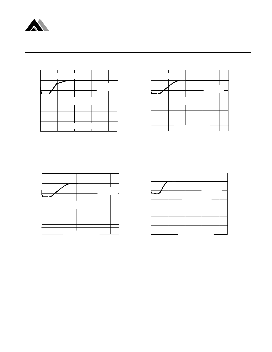
Chip Enable Transient Response
Output (1V/DIV) Enable (2V/DIV)
TIME ( 1mS/DIV)
C
L
=2
µ
F
R
L
=10
C
B Y P
=1000pF
0
0
0
0
Chip Enable Transient Response
TIME ( 1mS/DIV)
C
L
=2
µ
F
R
L
=10
Output (1V/DIV) Enable (2V/DIV)
0
5
10
15
20
25
30
35
40
45
0
1
2
3
4
5
6
7
8
Ground Current vs. Input Voltage
Ground Current (
µ
µ
µ
µ
A)
Input Voltage (V)
85
O
C
25
O
C
Load Step ( 1mA-300mA)
I
L
(200mA/DIV) Vo(5mV/DIV)
TIME( 20mS/DIV)
C
L
=2.2
µ
F
C
I N
=2.2
µ
F
Output
I
L o a d
0
Analog Microelectronics, Inc.
9
AME8801/8812/8840
300mA CMOS LDO
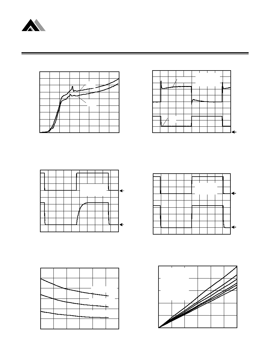
Overtemperature Shutdown
V
OUT
(1V/DIV) I
OUT
(200mA/DIV)
TIME (0.5Sec/DIV)
R
L O A D
=6.6
0
0
-80
-70
-60
-50
-40
-30
-20
-10
1.0E+01 1.0E+02 1.0E+03 1.0E+04 1.0E+05 1.0E+06
PSRR ( dB)
Power Supply Rejection Ratio
Frequency (Hz)
C
L
= 10
µ
F
Tantalum
I
L
= 100 mA
C
B Y P
= 0
C
B Y P
= 100 pF
C
B Y P
= 1 n F
C
B Y P
= 10 n F
-80
-70
-60
-50
-40
-30
-20
-10
1.0E+01
1.0E+02
1.0E+03
1.0E+04
1.0E+05
PSRR ( dB)
Power Supply Rejection Ratio
Frequency (Hz)
C
L
= 5.6
µ
F
Ceramic
I
L
= 100 mA
C
B Y P
= 0
C
B Y P
= 100 pF
C
B Y P
= 1 n F
C
B Y P
= 10 n F
-80
-70
-60
-50
-40
-30
-20
1.0E+01
1.0E+03
1.0E+05
1.0E+07
Power Supply Rejection Ratio
PSRR (dB)
Frequency (Hz)
C
L
=2.2
µ
F Tantalum
C
B Y P
=1000pF
1 0 0 m A
100
µ
A
1 m A
1 0 m A
1 0 0 m A
100
µ
A
-80
-70
-60
-50
-40
-30
-20
-10
0
1.0E+01
1.0E+03
1.0E+05
1.0E+07
Power Supply Rejection Ratio
PSRR (dB)
Frequency (Hz)
1 0 0 m A
1 0 m A
1 m A
100
µ
A
1 0 0 m A
100
µ
A
C
L
=2.2
µ
F Tantalum
C
B Y P
=0
Short Circuit Response
TIME (2mS/DIV)
V
OUT
(1V/DIV) I
LOAD
(400mA/DIV)
R
L O A D
=100
R
S H O R T
=0.1
0
0
Analog Microelectronics, Inc.
10
300mA CMOS LDO
AME8801/8812/8840
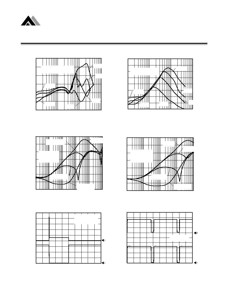
Noise Measurement
TIME (20mS/DIV)
Vo (1mV/ DIV)
Transient Line Response
TIME (2mS/DIV)
V
O
(1mV/DIV) V
IN
(1V/DIV)
C
L
= 2.2
µ
F
V
IN DC
= 5.0V
C
L
= 2.2
µ
F
NO FILTER
Current Limit Response
V
OUT
(1V/DIV) I
OUT
(200mA/DIV)
TIME (2mS/DIV)
R
L O A D
=3.3
0
0
10
100
300
0.1
1.0
8.0
SOT-23-5
Safe Operating Area
Output Current (mA)
Input-Output Voltage Differential (V)
Analog Microelectronics, Inc.
11
AME8801/8812/8840
300mA CMOS LDO
0.01
0.1
1
10
100
1000
10000
0
50
100
150
200
ESR (
)
Stable Region
Untested Region
Unstable Region
ILOAD (mA)
C
L
=1
µ
F
Stability vs. ESR vs I
LOAD
0.01
0.1
1
10
100
1000
10000
0
50
100
150
200
ILOAD (mA)
Stable Region
Untested Region
Unstable Region
ESR (
)
C
L
=2
µ
F
Stability vs. ESR vs I
LOAD
0.01
0.1
1
10
100
1000
10000
0
50
100
150
200
Stable Region
Untested Region
Unstable Region
ILOAD (mA)
ESR (
)
C
L
=3
µ
F
Stability vs. ESR vs I
LOAD
0.001
0.01
0.1
1
10
100
1000
10000
0
50
100
150
200
Stable Region
Untested Region
Unstable Region
ILOAD (mA)
ESR (
)
C
L
=10
µ
F
Stability vs. ESR vs I
LOAD

Analog Microelectronics, Inc.
12
300mA CMOS LDO
AME8801/8812/8840
Quiescent Current vs.Temp.
27
28
29
30
31
32
33
34
35
-45
-5
25
55
85
Temperature (
0
C)
Quiescent Current @ 5V (uA)
Load Regulation vs. Temp.
0.40
0.42
0.44
0.46
0.48
0.50
0.52
0.54
0.56
0.58
-45
-5
25
55
85
Temperature (
0
C)
Load Regulation (%)
Shut Down Current vs. Temp.
0.0
0.1
0.2
0.3
0.4
0.5
0.6
0.7
0.8
0.9
1.0
-45
-5
25
55
85
Temperature (
0
C)
Shut Down Current (uA)
Dropout Voltage vs. Temp.
1 5 0
1 6 0
1 7 0
1 8 0
1 9 0
2 0 0
2 1 0
2 2 0
-45
-5
2 5
5 5
8 5
Temperature (
0
C)
Dropout Voltage @ 300mA
(mV)
V
O U T
= 3 V
-0.50
-0.45
-0.40
-0.35
-0.30
-0.25
-0.20
-45
-5
25
55
85
Temperature (
0
C)
EN pin LO bias current (uA)
EN Pin LO Bias Current vs. Temp.
Analog Microelectronics, Inc.
13
AME8801/8812/8840
300mA CMOS LDO
n
n
n
n
n
Package Dimension
SOT-25
SOT-26
MIN
MAX
MIN
MAX
A
1.00
1.45
0.0394
0.0571
A
1
0.00
0.15
0.0000
0.0591
A2
0.70
1.25
0.0276
0.0492
b
0.35
0.55
0.0138
0.0217
C
0.08
0.25
0.0031
0.0098
D
2.70
3.10
0.1063
0.1220
E
1.40
1.80
0.0551
0.0709
e
H
2.60
3.00
0.1024
0.1181
L
0.30
-
0.0118
-
1
1
1
1
0
∞
10
∞
0
∞
10
∞
S
1
0.85
1.05
0.0335
0.0413
1.90 BSC
0.07480 BSC
SYMBOLS
MILLIMETERS
INCHES
MIN
MAX
MIN
MAX
A
1.00
1.40
0.0394
0.0551
A
1
0.00
0.15
0.0000
0.0591
A2
0.70
1.25
0.0276
0.0492
b
0.35
0.50
0.0138
0.0197
C
0.08
0.25
0.0031
0.0098
D
2.70
3.10
0.1063
0.1220
E
1.40
1.80
0.0551
0.0709
e
H
2.60
3.00
0.1024
0.1181
L
0.35
-
0.0138
-
1
0
∞
9
∞
0
∞
9
∞
S
1
0.85
1.05
0.0335
0.0413
1.90 BSC
0.0748 BSC
SYMBOLS
MILLIMETERS
INCHES
Life Support Policy:
These products of Analog Microelectronics, Inc. are not authorized for use as critical components in life-
support devices or systems, without the express written approval of the president
of Analog Microelectronics, Inc.
Analog Microelectronics, Inc. reserves the right to make changes in the circuitry and specifications of its
devices and advises its customers to obtain the latest version of relevant information.
©
Analog Microelectronics, Inc. , August 2001
Document: 2006-DS8801/8812/8840-E
Corporate Headquarters
Asia Pacific Headquarters
Analog Microelectronics, Inc.
AME, Inc.
3100 De La Cruz Blvd. Suite 201
2F, 187 Kang-Chien Road, Nei-Hu District
Santa Clara, CA. 95054-2046
Taipei 114, Taiwan, R.O.C.
Tel : (408) 988-2388
Tel : 886 2 2627-8687
Fax: (408) 988-2489
Fax : 886 2 2659-2989
www.analogmicro.com
E-Mail: info@analogmicro.com