 | –≠–ª–µ–∫—Ç—Ä–æ–Ω–Ω—ã–π –∫–æ–º–ø–æ–Ω–µ–Ω—Ç: AP1627 | –°–∫–∞—á–∞—Ç—å:  PDF PDF  ZIP ZIP |
AP1627
High-Efficiency Inverting Controller
This datasheet contains new product information. Anachip Corp. reserves the rights to modify the product specification without notice. No liability is assumed as a result of the use of
this product. No rights under any patent accompany the sale of the product.
Rev. 1.0 Sep 22, 2005
1/5
Features
- Input range: 2.5V ~ 6V
- Transformerless inverting controller
- Up to 400KHz operating frequency
- 1µA shutdown mode
- Drives high-side P-channel MOSFET
- 80% efficiency
- Soft-Start time set-up externally type
- MSOP-8L Pb-Free package
Applications
- Cell Phone
- Digital Cameras
- OLED Display Bios Voltage
General Description
The AP1627 is a high performance fixed frequency
about 400KHz PWM controllers. The controller was
specifically designed to be incorporated for step-up
and voltage inverting functions with a minimum
number of external components.
The AP1627 has a built-in 1.23V reference voltage;
a negative voltage can be set with the external
components. The soft-start time can be set with a
external capacitance.
The AP1627 are available in space-saving 8-pin
MSOP package. An evaluation kit is available to
expedite designs.
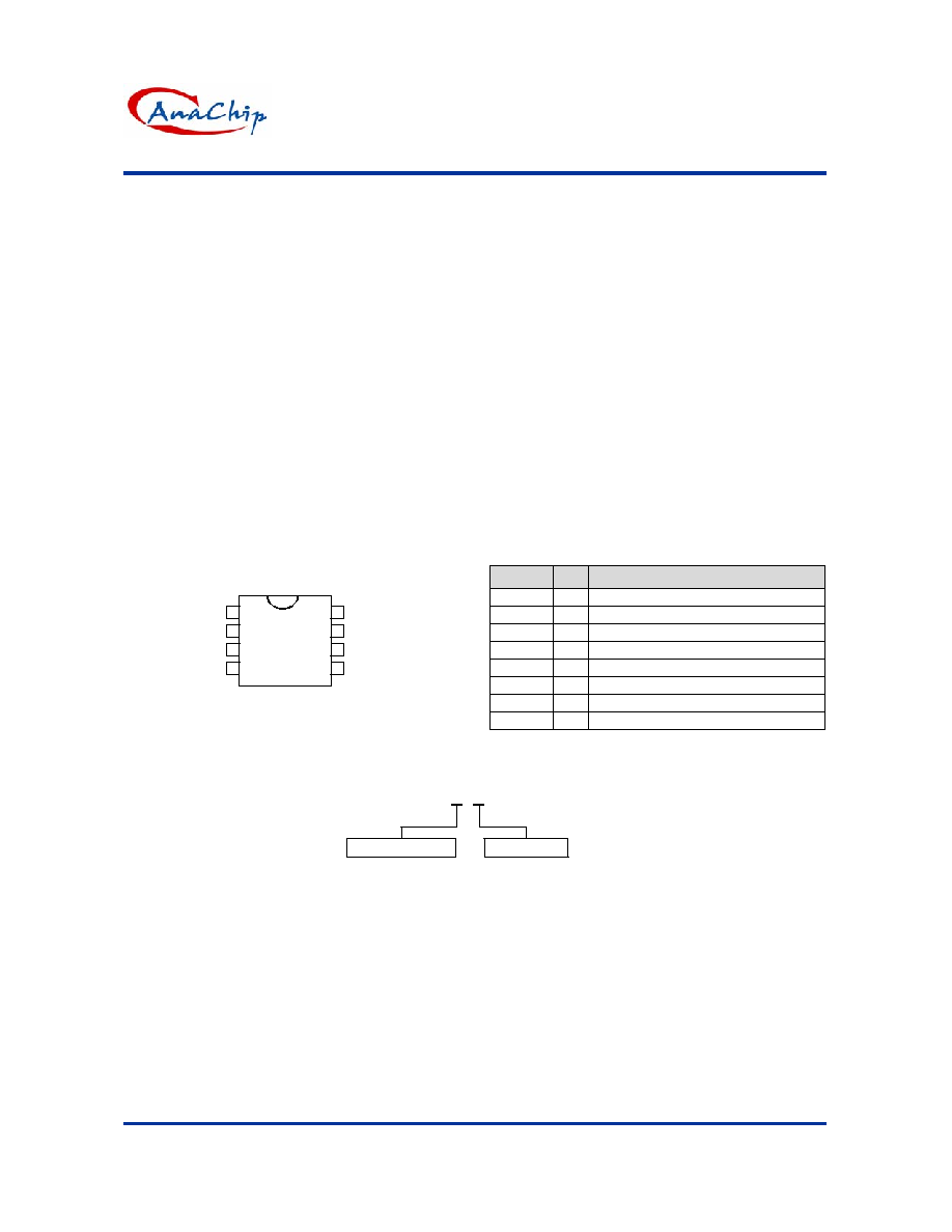
Pin Assignments
1
3
2
4
8
6
7
5
MSOP-8L
V
CC
FB
Comp
EXT
GND
CE
REF
SS
Pin Descriptions
Name
Pin
Description
V
CC
1 Power Input pin
FB 2 Feedback
Pin
REF
3 1.23 Reference Voltage
Comp
4 Compensation Pin
SS 5 Soft-Start
Pin
CE 6 Enable
Channel
GND 7 Signal
Ground
EXT
8 External P-MOSFET Connection
Ordering Information
AP 1627 X X
Package
Packing
M: MSOP-8L
Blank : Tube
A : Taping

AP1627
High-Efficiency Inverting Controller
Anachip Corp.
www.anachip.com.tw Rev. 1.0 Sep 22, 2005
2/5
Block Diagram
V
CC
EXT
REF
FB
Comp
GND
Soft
Start
REF
PMW
Control
CE
+
-
SS
CE
Absolute Maximum Ratings
Symbol
Parameter
Rating
Unit
V
CC
VIN Pin Voltage
-0.3 ~ 6.5
V
V
SS
SS Pin Voltage
-0.3 ~ V
CC
+0.3 V
V
COMP
Comp Pin Voltage
-0.3 ~ V
CC
+0.3 V
V
FB
FB Pin Voltage
-0.3 ~ V
CC
+0.3 V
V
CE
CE Pin Voltage
-0.3 ~ V
CC
+0.3 V
V
EXT
EXT PIN Voltage
-0.3 ~ V
CC
+0.3 V
I
EXT
EXT
PIN
Current
+100 mA
P
D
Continuous
Power
Dissipation
(T
A
= +40
o
C) 250
mW
T
OPR
Operating Temperature Range
-25 to +85
o
C
T
J
Junction Temperature
+140
o
C
T
STG
Storage Temperature Range
-40 to +125
o
C
Electrical Characteristics
AP1627 V
IN
=3.3V, V
OUT
= -9V, Load=100mA Ta=25
o
C
Parameter
Symbol
Conditions
Min.
Typ.
Max.
Units
Input Voltage
V
CC
2.5
-
6
V
Reference Voltage
V
REF
1.205
1.23
1.255
V
Reference Drift
T
A
=-25
o
C~85
o
C -
50
-
ppm/
o
C
Quiescent Current
I
CCQ
No external components,
CE=V
IN
,
V
FB
=-0.4V
- 50
100
µA
Stand-by Current
I
STB
No external components,
CE=0V,
V
FB
=-0.4V
- - 2 µA
Oscillator
Frequency Fosc
300 400 500 kHz
Maximum Duty Ratio MAXDTY
-
80
-
%
CE"High" Voltage
V
CEH
Apply above 0.65Vcc (min.) to CE,
Operating mode
0.65 - - *Vcc
CE"Low" Voltage
V
CEL
Apply under 0.2Vcc (min.) to CE,
Standby mode
- -
0.20
*Vcc
Line Regulation
V
CC
=3V~6V -
-
0.4
%
Load
Regulation
Load=0~400mA
- - 0.2 %
Efficiency EFFI
-
80
-
%

AP1627
High-Efficiency Inverting Controller
Anachip Corp.
www.anachip.com.tw Rev. 1.0 Sep 22, 2005
3/5
Typical Application Circuit
VCC
1
FB 2
Vref 3
Comp
4
SS
5
CE
6
VSS 7
EXT 8
U1
AP1627
C1
22uF
C10
33uF
C2
0.1uF
C3
0.1uF
C4
10nF
C5
10nF
C6
39pF
C7
0.1uF
C11
0.1uF
R3
100
R4
1M
R5
1M
R1
R2
VCC
Q1
AF2301
L1
10uH
D1
SS240
Vout
R2 suggest 50K~100K
Vref=1.23V
Vout = Vref * (R1/R2)
2.5~6V
Function Description
The AP1627 is an inverting controller that generates
a regulated negative output voltage, typically for
OLED display bias. This is useful in height-limited
designs where transformers may not be desired.
The MOSFET driver EXT in the AP1627 is designed
to drive P-channel MOSFETs.
Reference
The AP1627 has a precise 1.23V reference.
Connect a 0.1uF ceramic bypass capacitor from
REF to GND within 0.2in (5mm) of the REF pin.
REF can source up to 100µA and is enabled
whenever ON is high and V
CC
is above 2.5V. If the
100µA REF load limit must be exceeded, buffer
REF with an external op amp.
Shutdown
When CE voltage is lower than 0.2*Vcc, the internal
reference and biasing circuit totally turn off, the
output voltage drops to zero and the supply current
drops to 1uA.
Output Adjustable
The output voltage for the AP1627 is set by two
resistors, R1 and R2, which form a voltage divider
between the output, FB pin and REF pin, R2 can be
any value from 50K to 100K. R1 is given by the
following formula:
R1=
1.23
Vout
◊R2
Soft-Start
A capacitor connects with SS to GND. It can cause
the start-up current to rise preventing output voltage
overshoot slowly and high inrush current. The
capacitor value directly effect start-up time.
Duty Cycle
The maximum duty cycle of the AP1627 is 80%.
The duty cycle for a given application inverting
topology is given by:
Duty cycle=
Vout
Vcc
Vout
+

AP1627
High-Efficiency Inverting Controller
Anachip Corp.
www.anachip.com.tw Rev. 1.0 Sep 22, 2005
4/5
Applications Information
Designing a PC Board
Good PC board layout is important to achieve
optimal performance from the AP1627. Poor design
can cause excessive conducted and/or radiated
noise. Conductors carrying discontinuous currents
and any high-current path should be made as short
and wide as possible. A separate low-noise ground
plane containing the reference and signal grounds
should connect to the power-ground plane at only
one point to minimize the effects of power-ground
currents. Typically, the ground planes are best
joined right at the IC.
Keep the voltage-feedback network very close to
the IC, preferably within 0.2in (5mm) of the FB pin.
Nodes with high dV/dt (switching nodes) should be
kept as small as possible and should be routed
away from high-impedance nodes such as FB.
Marking Information
Logo
Part Number
ID code: internal
M: Month (A~L)
1627
YM X
(Top View)
Date code:
Y: Year : 0~9
AP1627
High-Efficiency Inverting Controller
Anachip Corp.
www.anachip.com.tw Rev. 1.0 Sep 22, 2005
5/5
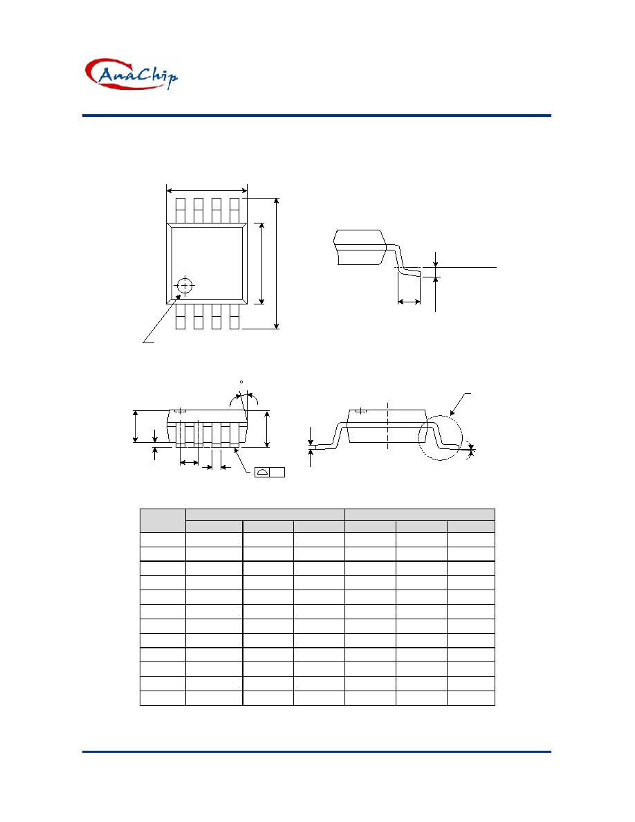
Package Information
Package Type: MSOP-8L
E1
E
D
L
GAGE PLANE
0.
25
DETAIL A
b
A2
A1
A
y
C
DETAIL A
e
12 (4x)
0.038DP SURFACE POLISHED
PIN 1 INDICATOR 0.45 mm
◊
Dimensions In Millimeters
Dimensions In Inches
Symbol
Min.
Nom.
Max.
Min.
Nom.
Max.
A 0.81 1.02
1.22
0.032
0.040
0.048
A1 0.05 - 0.15
0.002 - 0.006
A2 0.76 0.86 0.97
0.030
0.034
0.038
b 0.28 0.30
0.38
0.011
0.012
0.015
C 0.13 0.15
0.23
0.005
0.006
0.009
D 2.90 3.00
3.10
0.114
0.118
0.122
E 4.80 4.90
5.00
0.189
0.193
0.197
E1 2.90 3.00 3.10
0.114
0.118
0.122
e - 0.65
- -
0.0256
-
L 0.40 0.53
0.66
0.016
0.021
0.026
y -
- 0.076 - - 0.003
0∫ 3∫ 6∫ 0∫ 3∫ 6∫