 | –≠–ª–µ–∫—Ç—Ä–æ–Ω–Ω—ã–π –∫–æ–º–ø–æ–Ω–µ–Ω—Ç: AWT6102M2 | –°–∫–∞—á–∞—Ç—å:  PDF PDF  ZIP ZIP |
FEATURES
APPLICATIONS
9x11.6 mm
MCM Module Package
∑
InGaP HBT Technology
∑
High Efficiency 55% GSM
∑
High Efficiency 50% DCS
∑
High Efficiency 45% PCS
∑
Low Leakage Current ( <10
µ
A)
∑
SMT Module Package
∑
Small Foot Print (9.2mm X 11.6mm)
∑
Low Profile (1.55 mm)
∑
50
Input and Output Matching
∑
Minimum Number of External Components
Description
The AWT6102 is a 3.5V power amplifier module for use in dual Mode GSM/DCS/PCS wireless handsets and
communication systems.
∑
GSM/DCS Dual Band Handsets
∑
GSM/PCS Dual Band Handsets
∑
GSM/DCS/PCS Triple Band Handsets
AWT6102M2
EGSM/DCS/PCS Triple Band
Power Amplifier Module
Advanced Product Information Rev. 2
Absolute Minimum and Maximum Ratings
SIGNAL
MIN
MAX
UNITS
Supply Voltage (Vcc )
+7
V
Input Power (RF
IN
)
+15
dBm
Control Voltage (V
APC
)
+ 4.3V
V
Storage Temperature (T
STG
)
-55
150
∞C
Operating Temperature (T
C
)
-25
85
∞C
2
AWT6102M2
Electrical Specifications EGSM:
(Unless otherwise specified: V
cc
= 3.2V, Z
IN
= Z
OUT
=50
System, T
C
= 25 ∞C, pulsed operation with
577
µ
sec pulse width and 12.5% duty cycle)
PARAMETER
SYMBOL
MIN
TYP
MAX
UNITS
Frequency
fo
880
-
915
MHz
Supply Voltage
V
CC
2.9
3.2
4.5
V
Control Voltage Range
V
APC
0.2
2.0
2.7
V
Power Control Current
I
APC
1
mA
Input Power
P
IN
8
10
12
dBm
Output Power
P
OUT
34.5
-
dBm
Power Added Efficiency
PAE
50
55
-
%
Degraded Output Power
V
C C
=2.9 V, V
APC
= 2.4V,
P
IN
= 8dBm, T
C
= 85 ∞C
32
dBm
Isolation
V
APC
= 0.2V, P
IN
= 10 dBm
-25
-35
dBm
Harmonics
(1)
2
nd
3
rd
3fo to 12.750 GHz
-
-
-
-
-12
-15
-7
-7
-7
dBm
dBm
dBm
Stability: Load 8:1 VSWR
All phase angles
-
-
-70
dBc
Ruggedness: P
IN
= 12 dBm,
V
SUP
=4.5V, V
APC
= 0.2 - 2.8V
10:1 VSWR
All Phases
Leakage Current
V
APC
=0V, V
C C
= 4.5V
No input power
-
10
-
A
Noise Power
925 to 935 MHz
935 to 960 MHz
-72
-84
dBm/100 KHz
dBm/100 KHz
Switching Time
V
APC
on to 90% detected P
OUT
2
sec
Input VSWR
-
-
2:1
Output VSWR
2:1
µ
µ

3
AWT6102M2
Electrical Specifications DCS/PCS:
(Unless otherwise specified: V
cc
= 3.2V, Z
IN
= Z
OUT
=50
System, T
C
= 25 ∞C, pulsed operation with
577
µ
sec pulse width and 12.5% duty cycle)
PARAMETER
SYMBOL
MIN
TYP
MAX
UNITS
Frequency DCS
fo
1710
-
1785
MHz
Frequency PCS
fo
1850
-
1910
MHz
Supply Voltage
V
C C
2.9
3.2
4.5
V
Control Voltage Range
V
A P C
0.2
2.0
2.7
V
Power Control Current
I
APC
1
mA
Input Power
P
IN
6
8
10
dBm
Output Power DCS
P
OUT
31.5
-
dBm
Output Power PCS
P
OUT
TBD
-
dBm
Power Added Efficiency (DCS)
PAE
45
50
-
%
Power Added Efficiency (PCS)
PAE
TBD
TBD
-
%
Degraded Output Power (DCS/PCS)
V
C C
=2.9 V, V
APC
= 2.4V,
P
IN
= 6dBm, T
C
= 85 ∞C
29.5
dBm
Isolation
V
A P C
= 0.2V, P
IN
= 10 dBm
-30
-35
dBm
Harmonics
(1)
2
nd
3
rd
3fo to 12.750 GHz
-
-
-
-
-12
-15
-7
-7
-7
dBm
dBm
dBm
Stability: Load 8:1 VSWR
All phase angles
-
-
-70
dBc
Ruggedness: P
IN
= 10 dBm,
V
S U P
=4.5V, V
APC
= 0.2 - 2.8V
10:1 VSWR
All Phases
Leakage Current
V
A P C
=0V, V
C C
= 4.5V
No input power
-
10
-
A
Noise Power
20 MHz offset
-76
dBm/100 KHz
Switching Time
V
A P C
on to 90% detected P
OUT
2
sec
Input VSWR
-
-
2:1
Output VSWR
-
-
2:1
µ
µ
4
AWT6102M2
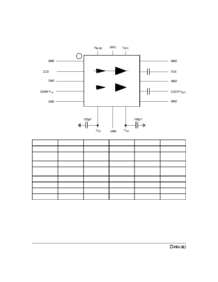
Schematic
Pin
Name
Description
Pin
Name
Description
1
GND
Ground
9
GND
Ground
2
DCS/PCS
DCS/PCS RF
Input Signal
10
EGSM P
OUT
GSM RF output
3
GND
Ground
11
GND
Ground
4
EGSM P
IN
GSM RF Input
Signal
12
DCS/PCS
DCS/PCS RF
output
5
GND
Ground
13
GND
Ground
6
V
CC
A
Supply Voltage
14
V
APC
Power Control
7
GND
Ground
15
GND
Ground
8
V
CC
B
Supply Voltage
16
V
BAND
(1)
Band Select
Notes:
1. Vband:
EGSM 0.0 to 0.5V
DCS/PCS: 2.0 to 2.8V
A
B
/ PCS
68 pF
/ PCS
1
33 pF
5
AWT6102M2
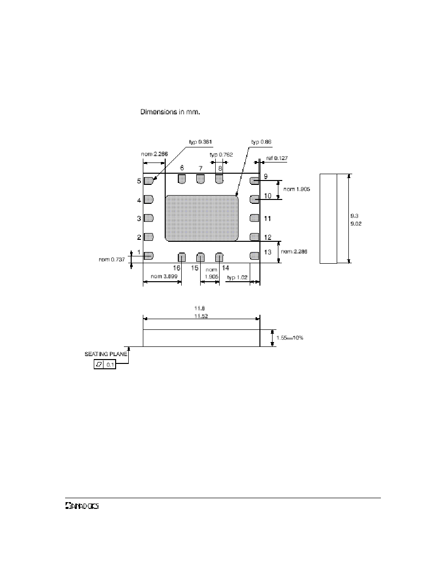
Package Outline Drawing
Bottom View