 | ÐлекÑÑоннÑй компоненÑ: APM2601 | СкаÑаÑÑ:  PDF PDF  ZIP ZIP |
Äîêóìåíòàöèÿ è îïèñàíèÿ www.docs.chipfind.ru
P-Channel Enhancement Mode MOSFET
Copyright ANPEC Electronics Corp.
Rev. A.1 - Jun., 2003
www.anpec.com.tw
1
ANPEC reserves the right to make changes to improve reliability or manufacturability without notice, and advise
customers to obtain the latest version of relevant information to verify before placing orders.
APM2601
Pin Description
Ordering and Marking Information
Features
Applications
Absolute Maximum Ratings
(T
A
= 25
°C unless otherwise noted)
·
-20V/-3A , R
DS(ON)
=80m
(typ.) @ V
GS
=-4.5V
R
DS(ON)
=110m
(typ.) @ V
GS
=-2.5V
··
··
·
Super High Dense Cell Design for Extremely
Low R
DS(ON)
··
··
·
Reliable and Rugged
··
··
·
SOT-23-6 Package
·
Power Management in Notebook Computer ,
Portable Equipment and Battery Powered
Systems.
Symbol
Parameter
Rating
Unit
V
DSS
Drain-Source Voltage
-20
V
GSS
Gate-Source Voltage
±8
V
I
D
*
Maximum Drain Current Continuous
-3
I
DM
Maximum Drain Current Pulsed
-10
A
* Surface Mounted on FR4 Board, t
10 sec.
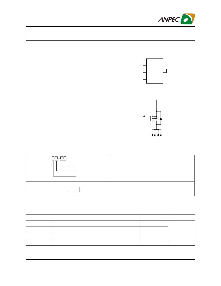
Top View of SOT-23-6
A P M 2601
H andling C ode
T em p. R an ge
P a ckage C o de
P a ckage C o de
C : S O T -23-6
O peration Junction T em p. R ange
C : -55 to 1 50 C
H andling C ode
T R : T ape & R eel
°
A P M 2601 C :
M 01X
X - D ate C ode
G
D
D
D
1
2
3
6
4
5
D
S
P-Channel MOSFET
G
D
S
D D D
Copyright ANPEC Electronics Corp.
Rev. A.1 - Jun., 2003
www.anpec.com.tw
2
APM2601
Notes
a
: Pulse test ; pulse width
300µs, duty cycle 2%
b
: Guaranteed by design, not subject to production testing
Absolute Maximum Ratings (Cont.)
(T
A
= 25
°C unless otherwise noted)
Symbol
Parameter
Rating
Unit
T
A
=25
°C
1.25
P
D
Maximum Power Dissipation
T
A
=100
°C
0.5
W
T
J
Maximum Junction Temperature
150
°C
T
STG
Storage Temperature Range
-55 to 150
°C
R
jA
Thermal Resistance Junction to Ambient
100
°C/W
APM2601
Symbol
Parameter
Test Condition
Min.
Typ.
Max.
Unit
Static
BV
DSS
Drain-Source Breakdown
Voltage
V
GS
=0V , I
DS
=-250
µA
-20
V
I
DSS
Zero Gate Voltage Drain
Current
V
DS
=-16V , V
GS
=0V
-1
µA
V
GS(th)
Gate Threshold Voltage
V
DS
=V
GS
, I
DS
=-250
µA
-0.45
-1.2
V
I
GSS
Gate Leakage Current
V
GS
=
±8V , V
DS
=0V
±100
nA
V
GS
=-4.5V , I
DS
=-3A
80
100
R
DS(ON)
a
Drain-Source On-state
Resistance
V
GS
=-2.5V , I
DS
=-2A
110
135
m
V
SD
a
Diode Forward Voltage
I
SD
=-1.25A , V
GS
=0V
-0.7
-1.3
V
Dynamic
b
Q
g
Total Gate Charge
6.4
8
Q
gs
Gate-Source Charge
1
Q
gd
Gate-Drain Charge
V
DS
=-10V , I
DS
=-1A
V
GS
=-4.5V
1.8
nC
t
d(ON)
Turn-on Delay Time
8
18
T
r
Turn-on Rise Time
4
10
t
d(OFF)
Turn-off Delay Time
20
45
T
f
Turn-off Fall Time
V
DD
=-10V , I
DS
=-1A ,
V
GEN
=-4.5V , R
G
=6
7
16
ns
C
iss
Input Capacitance
550
C
oss
Output Capacitance
265
C
rss
Reverse Transfer Capacitance
V
GS
=0V
V
DS
=-15V
Frequency=1.0MHz
115
pF
Electrical Characteristics
(T
A
= 25
°C unless otherwise noted)
Copyright ANPEC Electronics Corp.
Rev. A.1 - Jun., 2003
www.anpec.com.tw
3
APM2601
0
2
4
6
8
10
0.00
0.02
0.04
0.06
0.08
0.10
0.12
0.14
0.16
0.18
0.0
0.5
1.0
1.5
2.0
2.5
3.0
0
2
4
6
8
10
0
1
2
3
4
5
6
7
8
9
10
0
2
4
6
8
10
-50
-25
0
25
50
75
100 125 150
0.00
0.25
0.50
0.75
1.00
1.25
1.50
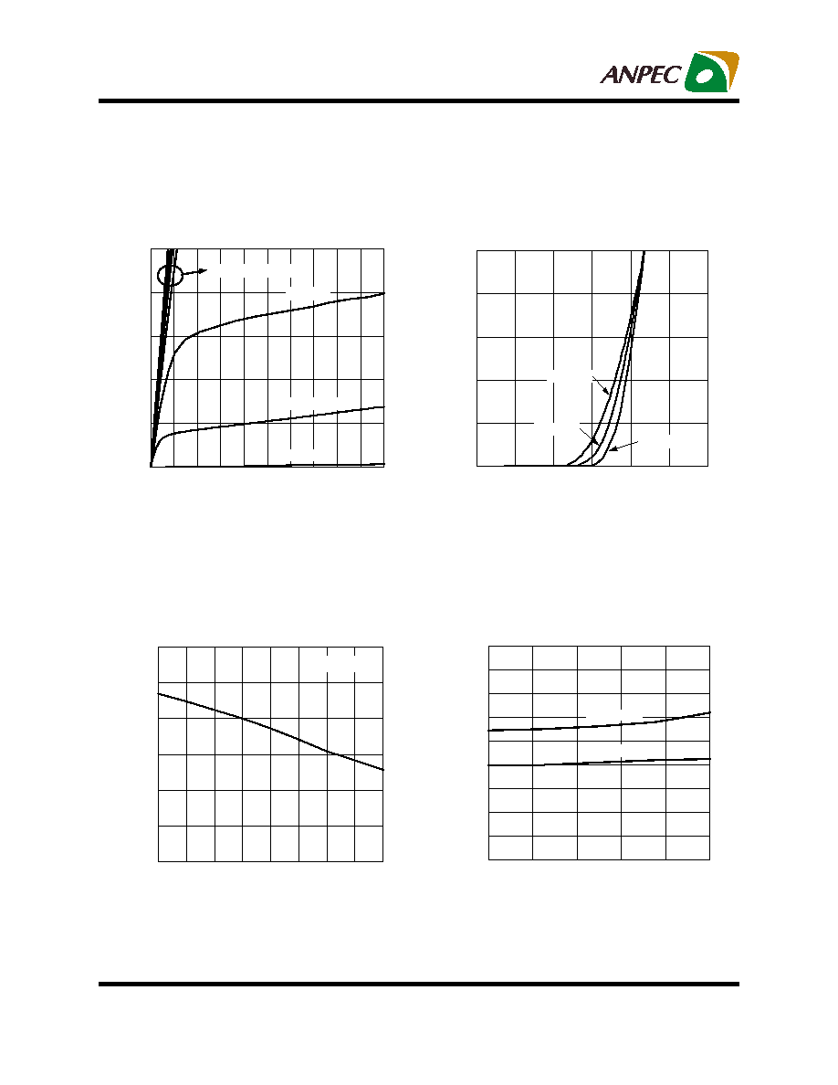
Typical Characteristics
-I
D-
Drain Current (A)
Transfer Characteristics
T
J
=-55°C
T
J
=25°C
T
J
=125°C
-V
GS
- Gate-to-Source Voltage (V)
Threshold Voltage vs. Junction Temperature
Tj - Junction Temperature (°C)
-V
GS(th)-
Threshold V
oltage (V)
(Normalized)
-I
DS
=250uA
R
DS(ON)
-On-Resistance (
)
On-Resistance vs. Drain Current
-V
GS
=2.5V
-I
D
- Drain Current (A)
-V
GS
=4.5V
-V
GS
=1V
Output Characteristics
-I
D
-Drain Current (A)
-V
GS
=3,4.5,6,7,8V
-V
GS
=2V
-V
DS
- Drain-to-Source Voltage (V)
-V
GS
=1.5V
Copyright ANPEC Electronics Corp.
Rev. A.1 - Jun., 2003
www.anpec.com.tw
4
APM2601
0
2
4
6
8
0
1
2
3
4
5
1
2
3
4
5
6
7
8
0.04
0.06
0.08
0.10
0.12
0.14
0.16
0.18
0.20
0
5
10
15
20
0
100
200
300
400
500
600
700
800
-50
-25
0
25
50
75
100 125 150
0.2
0.4
0.6
0.8
1.0
1.2
1.4
1.6
1.8
2.0
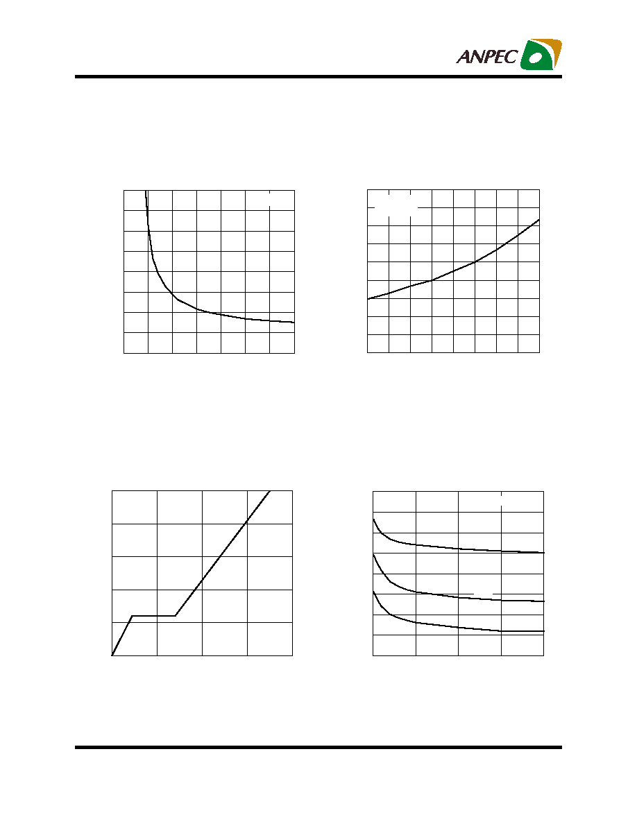
Typical Characteristics (Cont.)
R
DS(ON)
-On-Resistance (
)
(Normalized)
On-Resistance vs. Junction Temperature
-V
GS
=4.5V
-I
D
=3A
T
J
- Junction Temperature (°C)
-V
DS
- Drain-to-Source Voltage (V)
Capacitance
Capacitance (pF)
Ciss
Coss
Crss
-V
GS
- Gate-to-Source Voltage (V)
R
DS(ON)
-On-Resistance (
)
-I
D
=3A
On-Resistance vs. Gate-to-Source Voltage
Gate Charge
Q
G
- Gate Charge (nC)
-V
GS
-Gate-Source V
oltage (V)
-V
DS
=10V
-I
D
=1A
Frequency=1MHz
Copyright ANPEC Electronics Corp.
Rev. A.1 - Jun., 2003
www.anpec.com.tw
5
APM2601
0.0
0.2
0.4
0.6
0.8
1.0
1.2
1.4
1.6
1
10
0.01
0.1
1
10
100
0
2
4
6
8
10
12
14
1E-4
1E-3
0.01
0.1
1
10
100
0.01
0.1
1
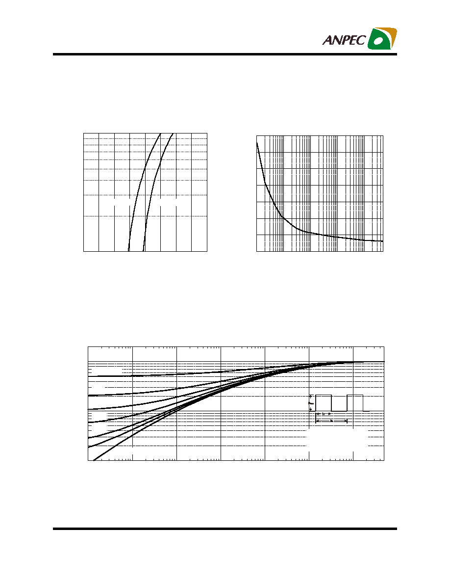
Typical Characteristics (Cont.)
Power (W)
Single Pulse Power
Time (sec)
Square Wave Pulse Duration (sec)
Source-Drain Diode Forward Voltage
-I
S
-Source Current (A)
T
J
=150°C
T
J
=25°C
-V
SD
-Source-to-Drain Voltage (V)
Normalized Effective Transient
Thermal Impedance
Normalized Thermal Transient Impedence, Junction to Ambient
1.Duty Cycle, D=t1/t2
2.Per Unit Base=R
thJA
=100°C/W
3.T
JM
-T
A
=P
DM
Z
thJA
Duty Cycle=0.5
D=0.2
D=0.1
D=0.05
D=0.02
SINGLE PULSE
D=0.01