 | –≠–ª–µ–∫—Ç—Ä–æ–Ω–Ω—ã–π –∫–æ–º–ø–æ–Ω–µ–Ω—Ç: EK01 | –°–∫–∞—á–∞—Ç—å:  PDF PDF  ZIP ZIP |
APEX MICROTECHNOLOGY CORPORATION ∑ TELEPHONE (520) 690-8600 ∑ FAX (520) 888-3329 ∑ ORDERS (520) 690-8601 ∑ EMAIL prodlit@apexmicrotech.com
INTRODUCTION
This easy-to-use kit provides a platform for the evaluation of
PWM amplifiers using the SA01 pin-out configuration. It can be used
to analyze a multitude of standard or proprietary circuit configura-
tions, and is flexible enough to do most standard amplifier test
configurations. The board is designed for surface mounting all
components except the switching amplifier.
The schematic is shown in Figure 2. Note that all of the compo-
nents shown on the schematic will probably not be used for any
single circuit. Some components will simply be omitted, while others
require installation of a jumper to complete the signal path.
Only components unique to the EK01 are provided in this kit.
Hardware similar to that shown in figure 1 must be obtained locally.
The PC board and the foot print of the heatsink measure 3" by 5".
PARTS LIST
Part #
Description
Quantity
HS16
Heatsink
1
MS04
PC mount Cage Jacks
1 Bag/12 each
EK01PC
PC Board
1
60SPG00001
Spacer Grommets
4
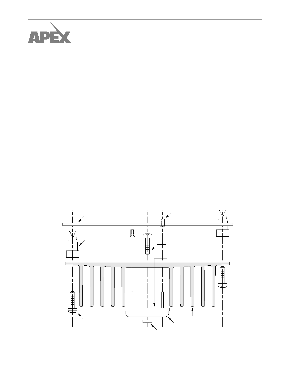
ASSEMBLY
1. From the non-silk screen side, insert and solder cage jacks. Be
sure each one is fully seated.
2. From the non-silk screen side, push spacer grommets into PC
board until fully seated. Grommets will snug when screws are
inserted for heatsink mounting.
3. Apply TW10 thermal washer or a thin, even coat of thermal
grease to the bottom of the SA01. If grease is from a tube make
sure there is no sign separation of solids and liquids. If from a jar,
stir it prior to application.
4. Use #14 sleeving to insulate and align at least 2 opposite pins of
the amplifier.
5. Mount amplifier to heatsink using #6 screws and nuts. Do not
over torque.
6. Install components as needed. External connections may be
soldered directly or standard banana jacks may be soldered to
these pads.
7. Insert amplifier pins into cage jacks and fasten board to heatsink.
TW10
Thermal Washer
1 Box/10 each
BEFORE YOU GET STARTED
*
All Apex amplifiers should be handled using proper ESD precautions.
*
Always use the heatsink included in this kit with thermal grease.
*
Torque the part to the specified 8 to 10 in-lbs (.9 to 1.13 N*M)
*
Always use adequate power supply bypassing.
*
Do not change connections while the circuit is powered.
*
Initially set all power supplies to the minimum operating levels allowed in the device data sheet.
*
Check for oscillations.
Heatsink
Switching Amplifier
Hex Nut 6-32 THD 1/4"
#8 or #10 Screw (1/2" - 3/4" LG)
Spacer Grommet
6-32 x 1/2 Lg. Screw
TW10 thermal washer or
thermal grease as required
PC Board (Silkscreen side)
FIGURE 1.
Cage Jack
Solder as required
H T T P : / / W W W . A P E X M I C R O T E C H . C O M ( 8 0 0 ) 5 4 6 - A P E X ( 8 0 0 ) 5 4 6 - 2 7 3 9
M I C R O T E C H N O L O G Y
EVALUATION KIT FOR SA01 PIN-OUT
EK01

APEX MICROTECHNOLOGY CORPORATION ∑ 5980 NORTH SHANNON ROAD ∑ TUCSON, ARIZONA 85741 ∑ USA ∑ APPLICATIONS HOTLINE: 1 (800) 546-2739
EVALUATION KIT
FOR SA01 PIN-OUT
EK01
TYPICAL COMPONENT FUNCTIONS
R1 Provides -IN bias from the Reference voltage.
R2 Sets DC scaling for external feedback such as tachometers, position sensors or current sensors.
R3 With R4 sets DC operating point of +IN, with R13 and R15 sets gain of voltage feedback circuit.
R4 With R3 sets DC operating point of +IN.
R5 Input scaling of the control signal.
R6 With C6 sets the corner frequency of the integrator.
R7 With C3 & C4 forms a low pass filter for the external feedback loop. Often used with tachometers.
R8 With C2 forms a low pass filter for the current limit circuit.
R9 Current sense. Often is a piece of resistance wire.
R10 With R8 divides shutdown signal voltage feeding SHDN/FILTER pin.
R11 With C5 sets corner frequency for external feedback loop.
R12, 13, 15, 16 Provides voltage feedback for a voltage controlled output.
R14 Helps set gain or scale input voltage levels.
R17 With C12 provides low pass filtering of +IN signal.
C1 Power supply bypass.
C2 With R8 form a low pass filter for the current limit circuit, also filters the SHDN signal.
C3, 4 With R7 forms a low pass filter for the external feed back loop. Often used with tachometers.
C5 With R11 sets corner frequency for external feedback loop.
C6 With R6 sets the corner frequency of the integrator.
C7 Power supply bypass, must have very low ESR in MHz range.
C8 Filters reference or feedback voltage at +IN.
C9 Bypass for the reference voltage.
C10, 11 With R15 and R16 provides low pass filtering of voltage feedback.
C12 With R17 provides low pass filtering of +IN signal.
C13 Provides AC coupling of +IN signal.
D1 ≠ D4 Optional flyback diodes.
D5 ≠ D7 Input protection zener diodes.
FIGURE 2. PCB SCHEMATIC.
EA
PWM
+V
S
EA
OUT
≠IN
7.5V
REF
+IN
GND
SHDN/
FILTER
I
SENSE
A
OUT
B
OUT
SA01
1
5
2
3
7
6
9
4
8
10
+V
S
A
OUT
B
OUT
GND
C2
R13
R15
R16
C8
R4
R17
C9
C13
R14
R1
R5
C3
R7
C4
R11
C5
R2
R6
C6
C1
D4
C7
R12
R3
R8
R9
SHDN
SIG
TACH/
FEEDBACK
SIG
≠IN
REF
OUT
GND
+IN
R10
C10
C11
C12
D1
D5
D2
D6
D3
11V
D7
11V
11V

APEX MICROTECHNOLOGY CORPORATION ∑ TELEPHONE (520) 690-8600 ∑ FAX (520) 888-3329 ∑ ORDERS (520) 690-8601 ∑ EMAIL prodlit@apexmicrotech.com
EK01
EVALUATION KIT
FOR SA01 PIN-OUT
FIGURE 3. PCB FRONT.
OPEN LOOP OPERATION
EA
PWM
+V
S
EA
OUT
≠IN
7.5V
REF
+IN
GND
SHDN/
FILTER
I
SENSE
A
OUT
B
OUT
SA01
1
5
2
3
7
6
9
4
8
10
+V
S
A
OUT
≠IN
+2.5/+7.5
B
OUT
GND
C2
R10
C9
R17
C12
C1
C6
R6
C7
R8
R9
SHDN
SIG
REF
OUT
V
IN
Duty Cycle @ A
OUT
2.5V 0%
5V 50%
7.5V 100%
V
IN
≠ 5
2.5
(A ≠ B) =
* V
S ≠
I
O
*
R
DSON
APEX MICROTECHNOLOGY CORPORATION ∑ 5980 NORTH SHANNON ROAD ∑ TUCSON, ARIZONA 85741 ∑ USA ∑ APPLICATIONS HOTLINE: 1 (800) 546-2739
EK01
COMMON
CONFIGURATIONS
EA
PWM
+V
S
EA
OUT
≠IN
7.5V
REF
+IN
GND
SHDN/
FILTER
I
SENSE
A
OUT
B
OUT
SA01
1
5
2
3
7
6
9
4
8
10
+V
S
A
OUT
B
OUT
GND
C2
R10
C8
R4
C9
R1
R17
R5
C3
R7
C4
R11
C5
R2
R6
C6
C1
C7
R3
R8
R9
SHDN
SIG
TACH/
FEEDBACK
SIG
REF
OUT
+IN
M
T
EA
PWM
+V
S
EA
OUT
≠IN
7.5V
REF
+IN
GND
SHDN/
FILTER
I
SENSE
A
OUT
B
OUT
SA01
1
5
2
3
7
6
9
4
8
10
+V
S
A
OUT
B
OUT
GND
C2
R10
C8
R4
C9
R1
R5
R7
R11
R17
C5
R2
R6
C6
C1
C7
R3
R8
R9
SHDN
SIG
TACH/
FEEDBACK
SIG
REF
OUT
+IN
+REF
≠REF
M
POSITION CONTROL
VOLTAGE CONTROL
SPEED CONTROL
EA
PWM
+V
S
EA
OUT
≠IN
7.5V
REF
+IN
GND
SHDN/
FILTER
I
SENSE
A
OUT
B
OUT
SA01
1
5
2
3
7
6
9
4
8
10
+V
S
A
OUT
B
OUT
GND
C2
R10
R13
C8
R4
C9
R1
R
O
R
O
R
I
R
F
R
F
R5
R17
R6
C6
C1
C7
R12
R3
R8
R9
SHDN
SIG
SIG
REF
OUT
R
F
R
I
(A ≠ B) = V
IN
*
R15
R16
C10
C11
This data sheet has been carefully checked and is believed to be reliable, however, no responsibility is assumed for possible inaccuracies or omissions. All specifications are subject to change without notice.
EK01U REV. C JANUARY 1998
© 1998 Apex Microtechnology Corp.