 | –≠–ª–µ–∫—Ç—Ä–æ–Ω–Ω—ã–π –∫–æ–º–ø–æ–Ω–µ–Ω—Ç: PA16U | –°–∫–∞—á–∞—Ç—å:  PDF PDF  ZIP ZIP |
APEX MICROTECHNOLOGY CORPORATION ∑ TELEPHONE (520) 690-8600 ∑ FAX (520) 888-3329 ∑ ORDERS (520) 690-8601 ∑ EMAIL prodlit@apexmicrotech.com
FEATURES
∑ HIGH POWER BANDWIDTH -- 350kHz
∑ HIGH SLEW RATE -- 20V/
µ
s
∑ FAST SETTLING TIME -- 600ns
∑ LOW CROSSOVER DISTORTION -- Class A/B
∑ LOW INTERNAL LOSSES -- 1.2V at 2A
∑ HIGH OUTPUT CURRENT --
±
5A PEAK
∑ LOW INPUT BIAS CURRENT -- FET Input
∑ ISOLATED CASE -- 300 VDC
APPLICATIONS
∑ MOTOR, VALVE AND ACTUATOR CONTROL
∑ MAGNETIC DEFLECTION CIRCUITS UP TO 5A
∑ POWER TRANSDUCERS UP TO 350 kHz
∑ AUDIO AMPLIFIERS UP TO 44W RMS
DESCRIPTION
The PA16 and PA16A are wideband, high output current
operational amplifiers designed to drive resistive, inductive
and capacitive loads. Their complementary "collector output"
stage can swing close to the supply rails and is protected
against inductive kickback. For optimum linearity, the output
stage is biased for class A/B operation. The safe operating
area (SOA) can be observed for all operating conditions by
selection of user programmable, current limiting resistors
(down to 10mA). Both amplifiers are internally compensated
but are not recommended for use as unity gain followers. For
continuous operation under load, mounting on a heatsink of
proper rating is recommended.
These hybrid integrated circuits utilize thick film (cermet)
resistors, ceramic capacitors and semiconductor chips to
maximize reliability, minimize size and give top performance.
Ultrasonically bonded aluminum wires provide reliable inter-
connections at all operating temperatures.
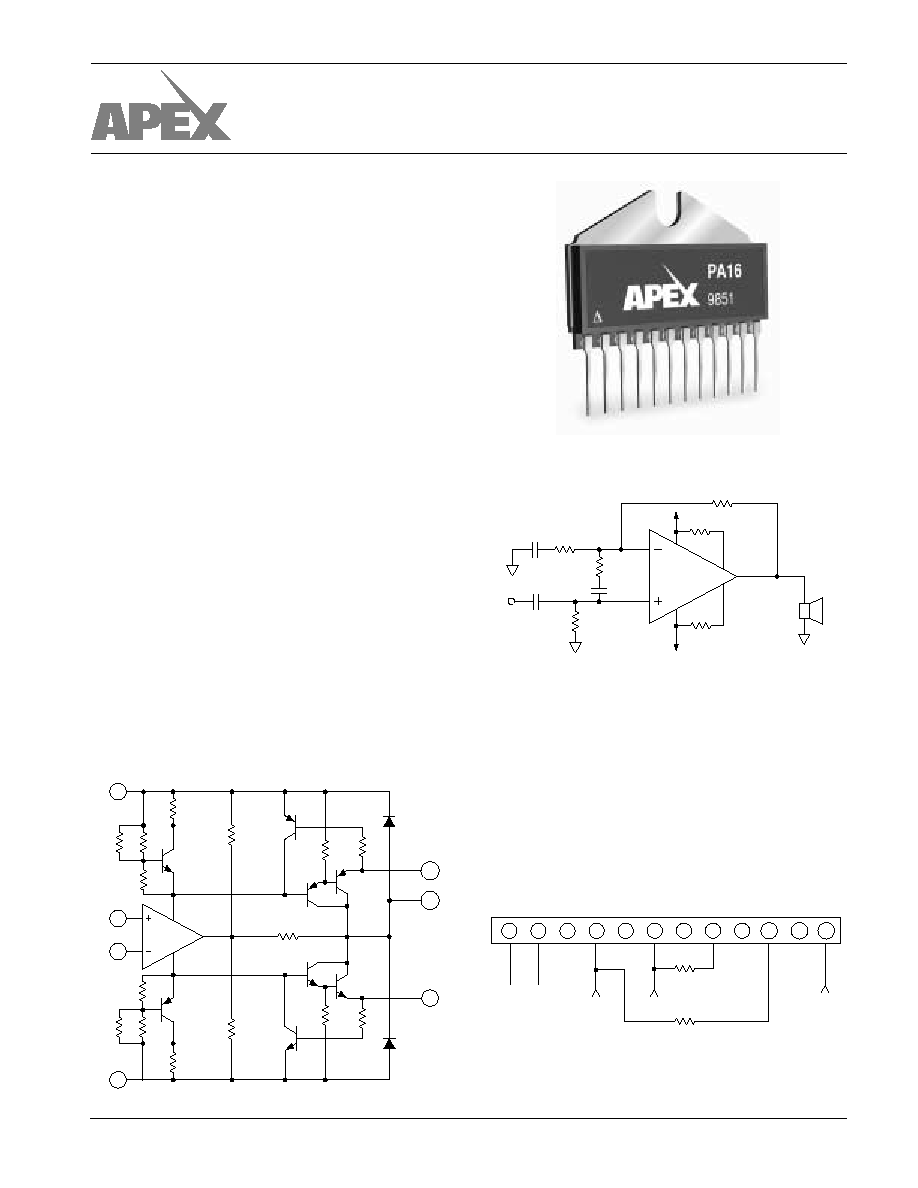
EQUIVALENT SCHEMATIC
TYPICAL APPLICATION
Vehicular Sound System Power Stage
When system voltages are low and power is at a premium,
the PA16 is a natural choice. The circuit above utilizes not only
the feature of low internal loss of the PA16, but also its very low
distortion level to implement a crystal clear audio amplifier
suitable even for airborne applications. This circuit uses AC
coupling of both the input signal and the gain circuit to render
DC voltage across the speaker insignificant. The resistor and
capacitor across the inputs form a stability enhancement
network. The 0.27 ohm current limit resistors provide protec-
tion in the event of an output short circuit.
16K
100K
R
CL+
R
CL≠
.27
.27
3.2
16W
≠12
+12
.47
µ
F
.47
µ
F
16K
.001
µ
F
PA16
IN
1K
LOW INTERNAL LOSS MAXIMIZES EFFICIENCY
H T T P : / / W W W . A P E X M I C R O T E C H . C O M ( 8 0 0 ) 5 4 6 - A P E X ( 8 0 0 ) 5 4 6 - 2 7 3 9
M I C R O T E C H N O L O G Y
POWER OPERATIONAL AMPLIFIERS
PA16 ∑ PA16A
R2
R3
R1
R5
R4
R8
R9
R10
R11
R12
R13
R14
R15
R6
R7
Q1
Q8
Q5
Q4
Q3
Q6
Q2
Q7
A1
D1
D2
4
2
1
6
8
12
10
≠IN
+IN
OUT
+V
≠R
CL
+R
CL
S
≠V
S
1
2
3
4
5
6
7
8
9
10
11
12
EXTERNAL CONNECTIONS
Package: SIP03
APEX MICROTECHNOLOGY CORPORATION ∑ 5980 NORTH SHANNON ROAD ∑ TUCSON, ARIZONA 85741 ∑ USA ∑ APPLICATIONS HOTLINE: 1 (800) 546-2739
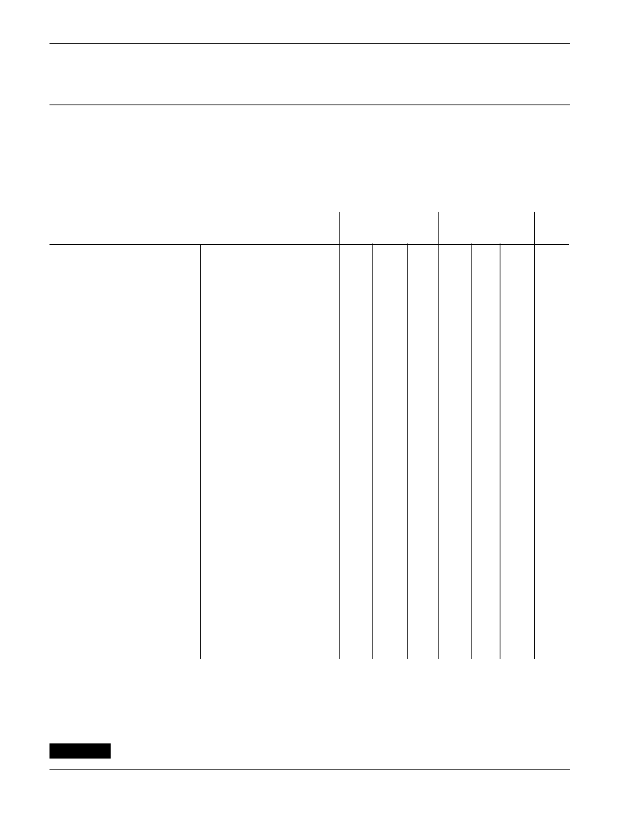
ABSOLUTE MAXIMUM RATINGS
SPECIFICATIONS
ABSOLUTE MAXIMUM RATINGS
SUPPLY VOLTAGE, +V
S
to ≠V
S
38V
OUTPUT CURRENT, within SOA
5A
POWER DISSIPATION, internal
1
62.5W
INPUT VOLTAGE, differential
±
V
S
≠5V
INPUT VOLTAGE, common mode
±
V
S
≠2V
TEMPERATURE, pin solder - 10s
300
∞
C
TEMPERATURE, junction
1
150
∞
C
TEMPERATURE RANGE, storage
≠65 to +150
∞
C
OPERATING TEMPERATURE RANGE, case ≠55 to +125
∞
C
PA16 ∑ PA16A
The exposed substrate contains beryllia (BeO). Do not crush, machine, or subject to temperatures in excess of 850
∞
C to
avoid generating toxic fumes.
CAUTION
SPECIFICATIONS
PARAMETER
TEST CONDITIONS
2, 6
MIN
TYP
MAX
MIN
TYP
MAX
UNITS
INPUT
OFFSET VOLTAGE, initial
T
C
= 25
∞
C
±
5
±
10
±
1
±
3
mV
OFFSET VOLTAGE, vs. temperature
Full temperature range
±
10
±
50
*
±
25
µ
V/
∞
C
OFFSET VOLTAGE, vs. supply
T
C
= 25
∞
C
±
10
*
µ
V/V
OFFSET VOLTAGE, vs. power
T
C
= 25
∞
C
±
6
*
µ
V/W
BIAS CURRENT, initial
T
C
= 25
∞
C
50
200
25
100
pA
BIAS CURRENT, vs. temperature
T
C
= 85
∞
C
200
*
pA/
∞
C
BIAS CURRENT, vs. supply
T
C
= 25
∞
C
.01
*
pA/V
OFFSET CURRENT, initial
T
C
= 25
∞
C
25
100
15
50
pA
OFFSET CURRENT, vs. temperature
T
C
= 85
∞
C
100
*
pA/
∞
C
INPUT IMPEDANCE, DC
T
C
= 25
∞
C
1000
*
G
INPUT CAPACITANCE
T
C
= 25
∞
C
3
*
pF
COMMON MODE VOLT. RANGE
5
, Pos. Full temperature range
+V
S
≠6
+V
S
≠3
*
*
V
COMMON MODE VOLT. RANGE
5
, Neg. Full temperature range
≠V
S
+6
≠V
S
+5
*
*
V
COMMON MODE REJECTION, DC
Full temperature range
70
100
*
*
dB
GAIN
OPEN LOOP GAIN at 10Hz
T
C
= 25
∞
C, 1k
load
103
*
dB
OPEN LOOP GAIN at 10Hz
Full temp. range, 10k
load
86
100
*
*
dB
GAIN BANDWIDTH PRODUCT at 1MHz T
C
= 25
∞
C, 10
load
4.5
*
MHz
POWER BANDWIDTH
T
C
= 25
∞
C, 10
load
350
*
kHz
PHASE MARGIN
Full temp. range, 10
load
30
*
∞
OUTPUT
VOLTAGE SWING
3
T
C
= 25
∞
C, I
O
= 5A, R
CL
= .08
±
V
S
≠4
±
V
S
≠3
±
V
S
≠3
*
V
VOLTAGE SWING
3
Full temp. range, I
O
= 2A
±
V
S
≠2
±
V
S
≠1.2
±
V
S
≠1.2
*
V
CURRENT, peak
T
C
= 25
∞
C
5
*
A
SETTLING TIME to .1%
T
C
= 25
∞
C, 2V step
.6
*
µ
s
SLEW RATE
T
C
= 25
∞
C
13
20
*
*
V/
µ
s
CAPACITIVE LOAD
Full temp. range, A
V
> 10
SOA
*
HARMONIC DISTORTION
P
O
= 5W, F = 1kHz, R
L
= 4
.028
*
%
SMALL SIGNAL rise/fall time
R
L
= 10
, A
V
= 1
100
*
ns
SMALL SIGNAL overshoot
R
L
= 10
, A
V
= 1
10
*
%
POWER SUPPLY
VOLTAGE
Full temperature range
±
7
±
15
±
19
*
*
*
V
CURRENT, quiescent
T
C
= 25
∞
C
27
40
*
*
mA
THERMAL
RESISTANCE, AC junction to case
4
F > 60Hz
1.4
1.6
*
*
∞
C/W
RESISTANCE, DC junction to case
F < 60Hz
1.8
2.0
*
*
∞
C/W
RESISTANCE, junction to air
30
*
∞
C/W
TEMPERATURE RANGE, case
Meets full range specifications
≠25
+85
*
*
∞
C
PA16A
PA16
NOTES:
*
The specification of PA16A is identical to the specification for PA16 in applicable column to the left.
1.
Long term operation at the maximum junction temperature will result in reduced product life. Derate internal power dissipation
to achieve high MTTF.
2.
The power supply voltage for all specifications is the TYP rating unless otherwise noted as a test condition.
3.
+V
S
and ≠V
S
denote the positive and negative supply rail respectively. Total V
S
is measured from +V
S
to ≠V
S
.
4.
Rating applies if the output current alternates between both output transistors at a rate faster than 60Hz.
5.
Exceeding CMV range can cause the output to latch.
6.
Full temperature specifications are guaranteed but not 100% tested.
APEX MICROTECHNOLOGY CORPORATION ∑ TELEPHONE (520) 690-8600 ∑ FAX (520) 888-3329 ∑ ORDERS (520) 690-8601 ∑ EMAIL prodlit@apexmicrotech.com
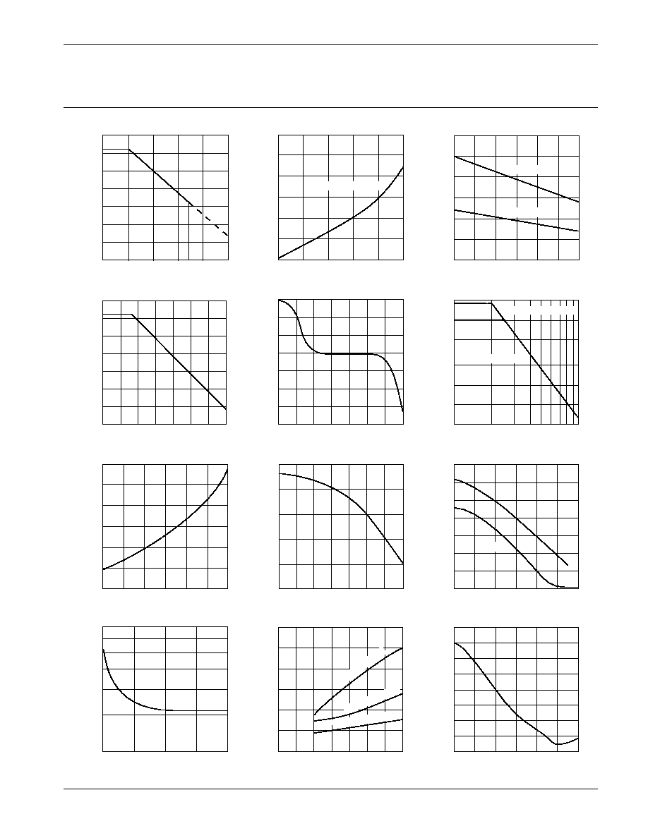
TYPICAL PERFORMANCE
GRAPHS
PA16 ∑ PA16A
0
25
50
75
100
125
CASE TEMPERATURE, T
C
(
∞
C)
0
30
50
70
POWER DERATING
INTERNAL POWER DISSIPATION, P
D
(W)
10
100
10K
.1M
FREQUENCY, F (Hz)
INPUT NOISE VOLTAGE, e
n
(nV/ Hz)
1
100
10M
FREQUENCY, F (Hz)
≠20
0
60
120
SMALL SIGNAL RESPONSE
OPEN LOOP GAIN, A
OL
(dB)
20
40
80
100
1
100
.1M
10M
≠210
≠150
≠60
0
PHASE RESPONSE
≠90
≠30
.1M
.2M
.5M
1M
FREQUENCY, F (Hz)
6
OUTPUT VOLTAGE, V (V )
O
1
3
4
7
OUTPUT CHANGE FROM ZERO, VOLTS
0
2
3
SETTLING TIME
TIME, t (
µ
S)
.5
1.5
2.5
0
OUTPUT CURRENT, I
O
(A)
OUTPUT VOLTAGE SWING
SATURATION VOLTAGE, V
S
≠
V
O
(V)
≠25
50
100
CASE TEMPERATURE, T (
∞
C)
0
2.5
CURRENT LIMIT
CURRENT LIMIT, I (A)
LIM
2.0
C
2
5
6
1.0
INPUT NOISE
1K
10
15
20
˜
1K
40
POWER RESPONSE
PP
.3M
0
25
75
.5
1.0
10
1K 10K .1M 1M
60
10
10K
1M
FREQUENCY, F (Hz)
PHASE, (
∞
)
1.5
.7M
7.8
10
13
18
23
30
1
125
3.0
≠180
≠120
25
30
35
40
1
2
3
4
5
1.5
2.0
2.5
3.0
3.5
8
1mV NO LOAD
10mV NO LOAD
.5
| +V
S
| + | ≠V
S
| = 36V
| +V
S
| + | ≠V
S
| = 30V
T
C
= 25 to 85
∞
C
±
V
O
R
CL
= 0.3
R
CL
= 0.62
10mV 10 LOAD
10
FREQUENCY, F(Hz)
POWER SUPPLY REJECTION
POWER SUPPLY REJECTION, PSR (dB)
100
1K
10K .1M
1M
10M
0
20
40
60
80
100
120
140
+V
S
≠V
S
≠25
CASE TEMPERATURE, Tc(
∞
C)
QUIESCENT CURRENT
NORMALIZED QUIESCENT CURRENT I
Q
(X)
0
25
50
75
100
125
.94
.92
.96
.98
1
1.02
1.04
1.06
1.08
1
10K
FREQUENCY, F (Hz)
COMMON MODE REJECTION
COMMON MODE REJECTION, CMR (dB)
40
80
120
.1M
10
100 1K
1M
20
60
100
10M
≠15
105
.25
64
256
BIAS CURRENT
4
.06
5
45
65
85
16
NORMALIZED BIAS CURRENT, I (X)
B
1
CASE TEMPERATURE, T (
∞
C)
C
25
10
20
APEX MICROTECHNOLOGY CORPORATION ∑ 5980 NORTH SHANNON ROAD ∑ TUCSON, ARIZONA 85741 ∑ USA ∑ APPLICATIONS HOTLINE: 1 (800) 546-2739
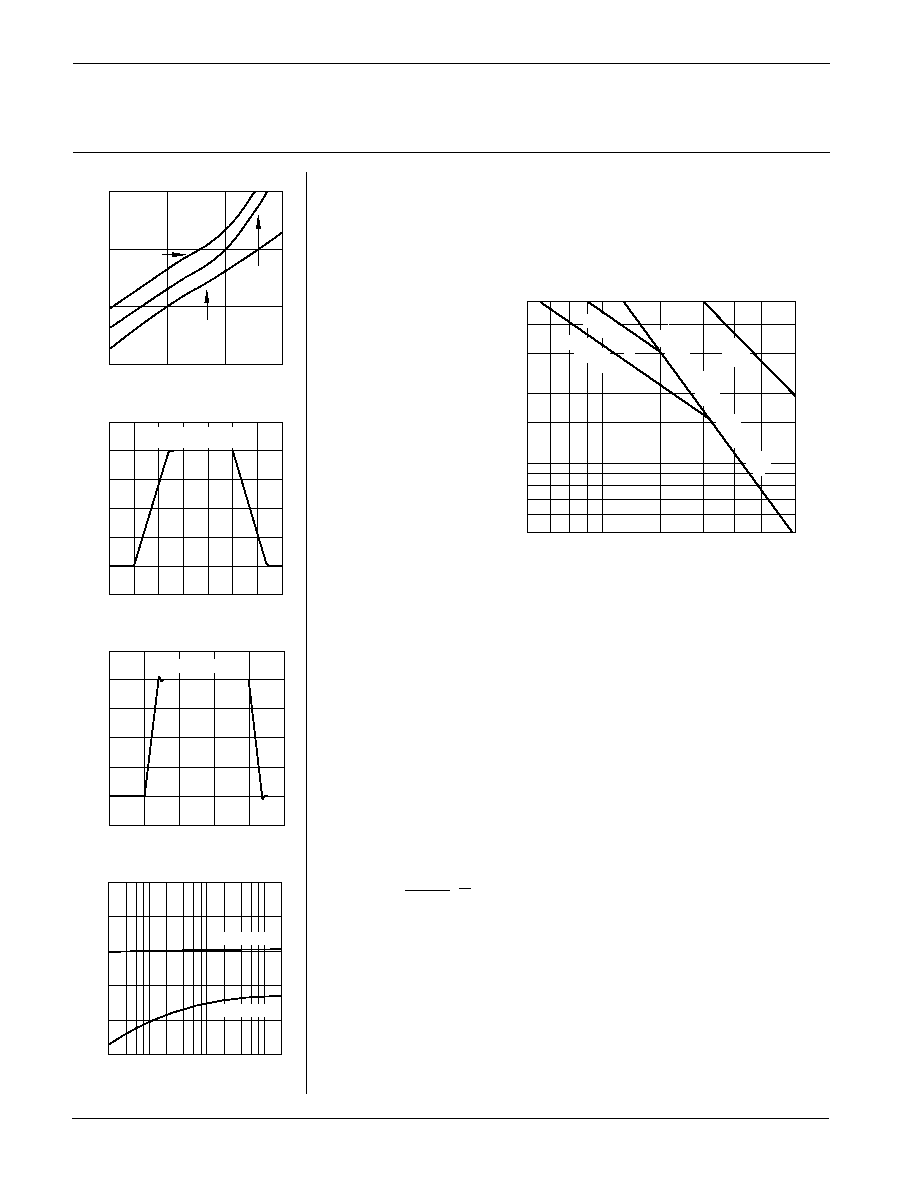
OPERATING
CONSIDERATIONS
PA16 ∑ PA16A
.1K
1.0K
FREQUENCY, F (Hz)
0.001
0.1
1
HARMONIC DISTORTION
DISTORTION, THD (%)
10K
0.01
100K
1
3
4
TIME, t (
µ
S)
≠15
5
15
PULSE RESPONSE
≠10
0
10
2
5
≠5
PULSE RESPONSE
OUTPUT VOLTAGE, V
O
(V)
≠.2
≠.1
0
.1
.2
.3
≠.3
10K
FREQUENCY, F (Hz)
LOADING EFFECTS
DELTA GAIN WITH LOAD, A (dB)
≠1.2
≠.6
0
.1M
100
1K
≠1.5
≠.9
≠.3
TIME, t (
µ
S)
0
.5
1.0
1.5
OUTPUT VOLTAGE, V
O
(V)
0
A
V
= 10
V
PS
=
±
15V
V
IN
=
±
.2V, tr = 50ns
V
IN
=
±
1V, tr = 100ns
LOAD = 10
I
O
= 150mA
I
O
= 400mA
P
O
= .5W
R
L
= 4
P
O
= 5W
R
L
= 4
P
O
= 25W
R
L
= 2
GENERAL
Please read Application Note 1 "General Operating Considerations" which covers
stability, supplies, heat sinking, mounting, current limit, SOA interpretation, and
specification interpretation. Visit www.apexmicrotech.com for design tools that help
automate tasks such as calculations for stability, internal power dissipation, current
limit; heat sink selection; Apex's complete Application Notes library; Technical Seminar
Workbook; and Evaluation Kits.
SAFE OPERATING
AREA (SOA)
The SOA curves com-
bine the effect of all limits
for this Power Op Amp.
For a given application,
the direction and magni-
tude of the output cur-
rent should be calculated
or measured and
checked against the SOA
curves. This is simple for
resistive loads but more
complex for reactive and
EMF generating loads.
The following guidelines
may save extensive ana-
lytical efforts:
The amplifier can handle any EMF generating or reactive load and short circuits to
the supply rails or shorts to common if the current limits are set as follows at
T
C
= 85
∞
C.
SHORT TO
±
V
S
SHORT TO
±
V
S
C, L OR EMF LOAD
COMMON
18V
.9A
1.8A
15V
1.0A
2.1A
10V
1.6A
3.2A
These simplified limits may be exceeded with further analysis using the operating
conditions for a specific application.
CURRENT LIMIT
Proper operation requires the use of two current limit resistors, connected as shown
in the external connection diagram. The minimum value for R
CL
is 0.12 ohm, however
for optimum reliability it should be set as high as possible. Refer to the "General
Operating Considerations" section of the handbook for current limit adjust details.
.65
I
LIM
(A)
0.01
R
CL
=
DEVICE MOUNTING
The case (mounting flange) is electrically isolated and should be mounted directly to
a heatsink with thermal compound. Screws with Belville spring washers are recom-
mended to maintain positive clamping pressure on heatsink mounting surfaces. Long
periods of thermal cycling can loosen mounting screws and increase thermal resis-
tance.
Since the case is electrically isolated (floating) with respect to the internal circuits it
is recommended to connect it to common or other convenient AC ground potential.
t = 5ms
steady
state second
breakdown
Tc = 60
∞
C
Tc = 85
∞
C
5.0
4.0
3.0
2.0
1.5
1.0
0.8
0.6
0.5
6
7
8
10
9
15
20
25
30
38
OUTPUT CURRENT FROM +V
S
OR
≠
V
S
(A)
SUPPLY TO OUTPUT DIFFERENTIAL VOLTAGE V
S
≠V
O
(V)
This data sheet has been carefully checked and is believed to be reliable, however, no responsibility is assumed for possible inaccuracies or omissions. All specifications are subject to change without notice.
PA16U REV. C FEBRUARY 2001
© 2001 Apex Microtechnology Corp.